Patent application title: P-I-N MICROCRYSTALLINE SILICON STRUCTURE OF THIN-FILM SOLAR CELLS AND METHOD FOR MANUFACTURING THE SAME
Inventors:
Yu-Hung Chen (Hsinchu, TW)
Jun-Chin Liu (Hsinchu, TW)
Chun-Heng Chen (Hsinchu, TW)
Assignees:
INDUSTRIAL TECHNOLOGY RESEARCH INSTITUTE
IPC8 Class:
USPC Class:
136255
Class name: Photoelectric cells schottky, graded doping, plural junction or special junction geometry
Publication date: 2013-10-24
Patent application number: 20130276871
Abstract:
A method for manufacturing a P-I-N microcrystalline silicon structure for
thin-film solar cells, includes the steps of: (a) forming a P-type layer;
(b) forming an I-type layer including a plurality of sub-layers
successively stacked on the P-type layer using gas mixtures including
fluoride and hydride that have different gas ratios, respectively; and
(c) forming an N-type layer on the I-type layer. First, second, and third
I-type sub-layers may be formed on the P-type layer using gas mixtures
including fluoride and hydride at a first, second, and third gas ratios,
respectively. Then, advantageously, the third gas ratio may be larger
than the second gas ratio and the second gas ratio may be larger than the
first gas ratio, and the first gas ratio may be 8%, the second gas ratio
may range between 15% and 35%, and the third gas ratio may range between
35% and 50%.Claims:
1. A method for manufacturing a P-I-N microcrystalline silicon structure
for thin-film solar cells, comprising the steps of: (a) forming a P-type
layer; (b) forming an I-type layer including a plurality of sub-layers
successively stacked on the P-type layer using gas mixtures including
fluoride and hydride that have different gas ratios, respectively; and
(c) forming an N-type layer on the I-type layer.
2. The method of claim 1, wherein step (b) includes: (i) forming a first I-type sub-layer on the P-type layer using a gas mixture including fluoride and hydride at a first gas ratio; and (ii) forming a second I-type sub-layer on the first I-type sub-layer using a gas mixture including fluoride and hydride at a second gas ratio.
3. The method of claim 2, wherein step (b) further includes: (iii) forming a third I-type sub-layer on the second I-type sub-layer using a gas mixture including fluoride and hydride at a third gas ratio.
4. The method of claim 3, wherein the third gas ratio is larger than the second gas ratio and the second gas ratio is larger than the first gas ratio.
5. The method of claim 3, wherein the third gas ratio is larger than the second gas ratio and the second gas ratio is larger than the first gas ratio, and wherein the first gas ratio is 8%, the second gas ratio ranges between 15% and 35%, and the third gas ratio ranges between 35% and 50%.
6. The method of claim 2, wherein the gas mixture used to form the first I-type sub-layer has a fluorine concentration ranging between 1E15 cm-3 and 1E21 cm.sup.-3.
7. The method of claim 2, wherein the second gas ratio is greater than the first gas ratio.
8. The method of claim 2, wherein the first I-type sub-layer has a crystallinity ranging between 45% and 80%.
9. The method of claim 1, wherein said fluoride is one of SiF4, SF6, CF4, CHF3, C2F6, C3F8, HF, CaF2, MgF2, BaF2 or a combination thereof.
10. The method of claim 1, wherein said hydride is one of SiH4 and Si2H6 or a combination thereof.
11. The method of claim 1, wherein the steps of forming the P-type layer, the I-type layer and the N-type layer are performed by a plasma-enhanced chemical vapor deposition (PECVD) technique.
12. A P-I-N microcrystalline silicon structure of thin-film solar cells, comprising: a P-type layer; an I-type layer including a plurality of stacked sub-layers successively formed on the P-type layer using gas mixtures including fluoride and hydride at different gas ratios; and an N-type layer formed on the I-type layer including the plurality of stacked sub-layers.
13. The structure of claim 12, wherein the I-type layer including a plurality of stacked sub-layers includes: a first I-type sub-layer formed on the P-type layer using a gas mixture including fluoride and hydride at a first gas ratio; and a second I-type sub-layer formed on the first I-type sub-layer using a gas mixture including fluoride and hydride at a second gas ratio.
14. The structure of claim 13, wherein the I-type layer including a plurality of stacked sub-layers further includes: a third I-type sub-layer formed on the second I-type sub-layer using a gas mixture including fluoride and hydride at a third gas ratio.
15. The structure of claim 14, wherein the third gas ratio is larger than the second gas ratio and the second gas ratio is larger than the first gas ratio.
16. The structure of claim 14, wherein the first gas ratio of fluoride to hydride is 8%, the second gas ratio of fluoride to hydride is between 15% and 80%, and the third gas ratio of fluoride to hydride is between 35% and 50%.
17. The structure of claim 13, wherein the concentration of fluorine in the gas mixture including fluoride and hydride at the first gas ratio is between 1E15 cm-3 and 1E21 cm.sup.-3.
18. The structure of claim 13, wherein the second gas ratio is greater than the first gas ratio.
19. The structure of claim 13, wherein the crystallinity of the first I-type sub-layer is between 45% and 80%.
20. The structure of claim 12, wherein fluoride is one of SiF4, SF6, CF4, CHF3, C2F6, C3F8, HF, CaF2, MgF2, BaF2 or a combination thereof.
21. The structure of claim 12, wherein hydride is one of SiH4 and Si2H6 or a combination thereof.
22. The structure of claim 12, wherein the P-type layer, the I-type layer or the N-type layer is formed by a plasma-enhanced chemical vapor deposition (PECVD) technique.
Description:
CROSS-REFERENCE TO RELATED APPLICATIONS
[0001] This application claims priority to Taiwanese Patent Application No. 101114082, filed on Apr. 20, 2012.
BACKGROUND
[0002] 1. Technical Field
[0003] The present disclosure relates to P-I-N microcrystalline silicon structures and methods for manufacturing the structures, and, more particularly, to a P-I-N microcrystalline silicon structure of thin-film solar cells and a method for manufacturing the structure.
[0004] 2. Description of Related Art
[0005] In a traditional P-I-N microcrystalline silicon structure of thin-film solar cells, the I-type layer is manufactured in a single step by mixing gas sources SiH4 and H2, wherein the amount of doped H2 in the total gas mixture is relatively high (for example, SiH4:H2 is 1:40), in order to enhance the crystallinity of the I-type layer. However, when the amount of the doped hydrogen is too high, the crystallinity will not increase accordingly. As a result, Voc and FF will drop, causing deterioration in efficiency of the component. Moreover, too much hydrogen is likely to cause damage in the P-type layer provided under the I-type layer.
[0006] A technique in which the I-type layer is formed through a single step with a gas mixture of SiF4, SiH4 and H2 has been proposed, whereby increasing nucleation of the I-type layer. Nonetheless, the erosion rate of fluoride is even higher than that of hydrogen, so despite that nucleation is increased through the single step with the addition of SiF4, the degree of damage caused at the interface between the I-type and P-type layers is widened, and internal defects in the I-type layer are also increased.
SUMMARY
[0007] The present disclosure effectively prevents interfacial damages between the I-type layer and the P-type layer, and reduces the internal defects in the I-type layer.
[0008] The present disclosure provides a method for manufacturing a P-I-N microcrystalline silicon structure of thin-film solar cells, which includes the following steps of: (1) forming a P-type layer; (2) forming an I-type layer including a plurality of sub-layers successively stacked on the P-type layer using gas mixtures including fluoride and hydride at different gas ratios; and (3) forming an N-type layer on the I-type layer including the plurality of stacked sub-layers.
[0009] In an embodiment of the present disclosure, step (2) includes: (2-1) forming a first I-type sub-layer on the P-type layer using a gas mixture including fluoride and hydride at a first gas ratio; and (2-2) forming a second I-type sub-layer on the first I-type sub-layer using a gas mixture including fluoride and hydride at a second gas ratio, and the second gas ratio is greater than the first gas ratio.
[0010] The present disclosure also provides a P-I-N microcrystalline silicon structure of thin-film solar cells, which includes: a P-type layer; an I-type layer including a plurality of stacked sub-layers successively formed on the P-type layer using gas mixtures including fluoride and hydride at different gas ratios; and an N-type layer formed on the I-type layer including the plurality of stacked sub-layers.
[0011] In an embodiment of the present disclosure, the I-type layer including a plurality of stacked sub-layers includes: a first I-type sub-layer formed on the P-type layer using a gas mixture including fluoride and hydride at a first gas ratio; and a second I-type sub-layer formed on the first I-type sub-layer using a gas mixture including fluoride and hydride at a second gas ratio, and the second gas ratio is greater than the first gas ratio.
[0012] Therefore, the present disclosure includes forming a first I-type sub-layer having fluoride and hydride with a lower fluoride ratio on a P-type layer, then a second I-type sub-layer having fluoride and hydride with a higher fluoride ratio is formed on the first I-type sub-layer, thus forming an I-type layer in several phases, and then an N-type layer is formed on top of the I-layer, thereby effectively preventing damages to the interface between the I-type layer and the P-type layer due to excessive fluoride, and also effectively reducing the internal defects within the I-type layer.
BRIEF DESCRIPTION OF THE DRAWINGS
[0013] The present disclosure can be more fully understood by reading the following detailed description of the embodiments, with reference made to the accompanying drawings, wherein:
[0014] FIG. 1 is a flow chart illustrating a method for manufacturing a P-I-N microcrystalline silicon structure of thin-film solar cells provided according to the present disclosure;
[0015] FIG. 2 is a schematic diagram depicting a P-I-N microcrystalline silicon structure of thin-film solar cells provided according to the present disclosure; and
[0016] FIG. 3 is a schematic diagram depicting another P-I-N microcrystalline silicon structure of thin-film solar cells provided according to the present disclosure.
DETAILED DESCRIPTION OF THE EMBODIMENTS
[0017] The present disclosure is described by the following specific embodiments. Those with ordinary skills in the arts can readily understand the other advantages and functions of the present disclosure after reading the disclosure of this specification. The present disclosure can also be implemented or applied with different embodiments.
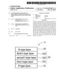
[0018] Referring now a flow chart shown in FIG. 1, a method for manufacturing a P-I-N microcrystalline silicon structure of thin-film solar cells is provided to facilitate understanding thereof.
[0019] In step S11, a P-type layer is formed. More specifically, the P-type layer is formed on a substrate by a plasma-enhanced chemical vapor deposition (PECVD) technique. Then, step S12 is performed.
[0020] In step S12, an I-type layer having a plurality of sub-layers is formed on the top of the P-type sub-layer by using a plurality of gas mixtures having fluoride and hydride at different gas ratios, wherein fluoride can be one of SiF4, SF6, CF4, CHF3, C2F6, C3F8, HF, CaF2, MgF2, BaF2 or a combination thereof, and hydride can be one of Sint and Si2H6 or a combination thereof. The step of forming the I-type layer can be carried out with a plasma-enhanced chemical vapor deposition (PECVD) technique. Then, step S13 is performed.
[0021] In step S13, an N-type layer is formed on the top of the I-type layer having a plurality of sub-layers by a plasma-enhanced chemical vapor deposition (PECVD) technique.
[0022] In an embodiment, in step S12 of forming an I-type layer having a plurality of sub-layers on the top of the P-type layer by using a plurality of gas mixtures having fluoride and hydride gases at different ratios, a first I-type sub-layer can be formed on the P-type layer using a gas mixture having fluoride and hydride at a first gas ratio, and then a second I-type sub-layer can be formed on the first I-type sub-layer using a gas mixture having fluoride and hydride at a second gas ratio greater than the first ratio.
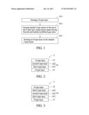
[0023] For example, as shown in FIG. 2, once a P-type layer 21 is formed, a first I-type sub-layer 221 is formed on the P-type layer 21 using a gas mixture having fluoride and hydride (e.g., SiF4/SiH4) at a gas ratio of 8%, and then a second I-type sub-layer 222 is formed on the first I-type sub-layer 221 using a gas mixture having SiF4/SiH4 at a gas ratio of 30%, thereby forming an I-type layer 22 in a P-I-N microcrystalline silicon structure with the stacked first I-type sub-layer 221 and second I-type sub-layer 222.
[0024] Furthermore, in an embodiment, in step S12, a first I-type sub-layer can be formed on the P-type layer using a gas mixture having fluoride and hydride at a first gas ratio, then a second I-type sub-layer can be formed on the first I-type sub-layer using a gas mixture having fluoride and hydride at a second gas ratio greater than the first gas ratio, and finally a third I-type sub-layer can be formed on the second I-type sub-layer using a gas mixture having fluoride and hydride at a third gas ratio greater than the second ratio.
[0025] For example, as shown in FIG. 3, once a P-type layer 31 is formed, a first I-type sub-layer 321 is formed on the P-type layer 31 using a gas mixture having fluoride and hydride (e.g., SiF4/SiH4) at a gas ratio of 8%, then a second I-type sub-layer 322 is formed on the first I-type sub-layer 321 using a gas mixture having SiF4/SiH4 at a gas ratio of 16%, and finally a third I-type sub-layer 323 is formed on the second I-type sub-layer 322 using a gas mixture having SiF4/SiH4 at a gas ratio of 24%, thereby forming an I-type layer 32 in a P-I-N microcrystalline silicon structure with the stacked first I-type sub-layer 321, the second I-type sub-layer 322 and third I-type sub-layer 323.
[0026] In addition, in an embodiment, the concentration of fluorine in the gas mixture having fluoride and hydride at the first gas ratio is between 1E15 cm-3 and 1E21 cm-3. The crystallinity of the first I-layers 221 and 321 can be between 45% and 80%. The gas mixtures can also contain a specific amount of H2. In actual implementations, the steps of forming sub I-layers can be added to increase the number of layers according to different requirements.
[0027] P-I-N microcrystalline silicon structures of thin-film solar cells provided according to the present disclosure can thus be those shown in FIGS. 2 and 3.
[0028] As shown in FIG. 2, a P-I-N microcrystalline silicon structure of thin-film solar cells 2 includes a P-type layer 21, an I-type layer having a plurality of sub-layers formed on the P-type layer 21, and an N-type layer 23 formed on the top of the I-type layer, wherein the plurality of sub-layers that form the I-layer are successively formed on the top of the P-type layer 21 respectively with gas mixtures having fluoride and hydride at different gas ratios.
[0029] More specifically, the plurality of sub-layers having the I-layer may include a first I-type sub-layer 221 and a second I-type sub-layer 222, wherein the first I-type sub-layer 221 is formed on the P-type layer 21 using a gas mixture having fluoride and hydride at a first gas ratio; and then the second I-type sub-layer 222 is formed on the first I-type sub-layer 221 using a gas mixture having fluoride and hydride at a second gas ratio.
[0030] As shown in FIG. 3, a P-I-N microcrystalline silicon structure of thin-film solar cells 3 includes a P-type layer 31, an I-type layer having a plurality of sub-layers formed on the P-type layer 31 and an N-type layer 33 formed on the top of the I-type layer, wherein the plurality of sub-layers that form the I-layer are successively formed on the top of the P-type layer 31 with respectively gas mixtures having fluoride and hydride at different gas ratios.
[0031] More specifically, the plurality of sub-layers having the I-layer may include a first I-type sub-layer 321, a second I-type sub-layer 322 and a third I-type sub-layer 323, wherein the first I-type sub-layer 321 is formed on the P-type layer 31 using a gas mixture having fluoride and hydride at a first gas ratio; the second I-type sub-layer 322 is formed on the first I-type sub-layer 321 using a gas mixture having fluoride and hydride at a second gas ratio; and the third I-type sub-layer 323 is formed on the second I-type sub-layer 322 using a gas mixture having fluoride and hydride at a third gas ratio.
[0032] Similar to the technical content disclosed in the disclosure of the manufacturing method above, the gas mixture having fluoride and hydride at the first gas ratio is a gas mixture having fluoride and hydride (SiF4/SiH4) at a gas ratio of 8%, for example; the gas mixture having fluoride and hydride at the second gas ratio is a gas mixture having SiF4/SiH4 at a gas ratio ranging between 15% and 35%, for example; and the gas mixture having fluoride and hydride at the third gas ratio is a gas mixture having SiF4/SiH4 at a gas ratio ranging between 35% and 50%, for example. In other words, the third ratio is greater than the second ratio, and the second ratio is larger than the first ratio. Other examples relating to concentrations, crystallinity, and compounds and depositions techniques used are the same as those previously mentioned, so they will not be further discussed.
[0033] In summary, the present disclosure includes forming a first I-type sub-layer having fluoride and hydride with a lower fluoride ratio on a P-type layer, thereby effectively preventing damages to the interface between the I-type layer and the P-type layer. Thereafter, a second I-type sub-layer having fluoride and hydride with a higher fluoride ratio is formed on the first I-type sub-layer, or a third I-type sub-layer having fluoride and hydride with an even higher fluoride ratio is further formed on the second I-type sub-layer. Finally, an N-type layer is formed on the top of the I-layer, thereby completing a P-I-N microcrystalline silicon structure. Since the I-type layer is formed in several phases by adjusting the gas ratio of fluoride and hydride, not only the P-type layer is prevented from damage, the internal defects within the I-type layer can be effectively reduced, increasing the yield of the product.
[0034] However, the above embodiments are only used to illustrate the principles of the present disclosure, and they should not be construed as to limit the present disclosure in any way. The above embodiments can be modified by those with ordinary skill in the art without departing from the scope of the present disclosure as defined in the following appended claims.
User Contributions:
Comment about this patent or add new information about this topic:
Images included with this patent application:
 |  |
| Similar patent applications: | |
| Date | Title |
|---|---|
| 2013-11-28 | Collector grid and interconnect structures for photovoltaic arrays and modules |
| 2013-11-28 | Integrated thin film photovoltaic module and manufacturing method thereof |
| 2013-11-28 | Thin film solar module and method for production of the same |
| 2013-06-13 | Crystalline silicon-based solar cell |
| 2013-11-28 | Solar cell and method of manufacture thereof, and solar cell module |
| New patent applications in this class: | |
| Date | Title |
|---|---|
| 2022-05-05 | Method of manufacturing -tandem photovoltaic cells and -tandem photovoltaic cell produced by this method |
| 2022-05-05 | Solar cell and method for manufacturing solar cell |
| 2019-05-16 | Solar cell and method for manufacturing the same |
| 2017-08-17 | Photoelectric conversion device and photoelectric conversion module |
| 2016-12-29 | Iii-v solar cell structure with multi-layer back surface field |
| New patent applications from these inventors: | |
| Date | Title |
|---|---|
| 2022-07-21 | Semiconductor device and method |
| 2022-03-31 | Gate oxide of nanostructure transistor with increased corner thickness |
| 2015-05-14 | Hit solar cell |
| 2014-10-23 | Solar cell with omnidirectional anti-reflection structure and method for fabricating the same |
| Top Inventors for class "Batteries: thermoelectric and photoelectric" | |
| Rank | Inventor's name |
|---|---|
| 1 | Devendra K. Sadana |
| 2 | Mehrdad M. Moslehi |
| 3 | Arthur Cornfeld |
| 4 | Seung-Yeop Myong |
| 5 | Bastiaan Arie Korevaar |