Patent application title: TAPE FOR ELECTRONIC DEVICES WITH REINFORCED LEAD CRACK
Inventors:
Dae Sung Yoo (Seoul, KR)
Han Mo Koo (Seoul, KR)
Ki Tae Park (Seoul, KR)
Jun-Young Lim (Seoul, KR)
Jun-Young Lim (Seoul, KR)
Tae Ki Hong (Seoul, KR)
Assignees:
LG INNOTEK CO., LTD.
IPC8 Class: AH05K702FI
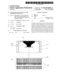
USPC Class:
361813
Class name: Housing or mounting assemblies with diverse electrical components for electronic systems and devices lead frame
Publication date: 2013-11-21
Patent application number: 20130308289
Abstract:
Provided is a tape for electronic devices with lead crack and a method of
manufacturing the tape. According to the present invention, by forming a
bending portion on a narrow circuit pattern to be connected from an inner
lead to an outer lead and further forming the bending portion within a
resin application portion, crack occurred in a narrow wiring width can be
avoided. The tape may include a first lead and a second lead formed on a
dielectric substrate and a bending portion formed on one of the first
lead and the second lead wherein the bending portion is formed within a
resin application portion.Claims:
1-18. (canceled)
19. A tape for electronic devices: a first lead and a second lead formed on a dielectric substrate; and a bending portion formed on one of the first lead and the second lead.
20. The tape for electronic devices of claim 19, wherein the bending portion has a structure in which the bending portion forms an angle of inclination with the second lead and in a longitudinal direction of the second lead.
21. The tape for electronic devices of claim 20, wherein the bending portion is formed on one of the first lead and the second lead.
22. The tape for electronic devices of claim 21, wherein the bending portion is less than one width of a width of the first lead and a width of the second lead.
23. The tape for electronic devices of claim 20, wherein at least one or more different distances among patterns of the first lead and the second lead exist.
24. The tape for electronic devices of claim 21, wherein the bending portion comprises a connecting pattern for the first lead and the second lead.
25. The tape for electronic devices of claim 24, wherein the connecting pattern connects the first lead and the second lead in a bending form.
26. The tape for electronic devices of claim 25, further comprising a resin application portion on the dielectric substrate.
27. The tape for electronic devices of claim 26, wherein the resin application portion is formed over a chip mounting portion on the dielectric substrate.
28. The tape for electronic devices of claim 26, wherein the bending portion is included within the resin application portion.
29. The tape for electronic devices of claim 28, wherein the width of the first lead and the width of the second lead are different from each other.
30. The tape for electronic devices of claim 29, wherein a pattern width of the first lead is wider than that of the second lead.
31. The tape for electronic devices of claim 28, further comprising an electronic device chip mounted to the chip mounting portion, and resin for burying a circumference of the electronic device chip in the resin application portion.
32. The tape for electronic devices of claim 31, wherein the resin is a potting material having viscosity.
33. The tape for electronic devices of claim 31, wherein the resin comprises epoxy.
34. The tape for electronic devices of claim 33, wherein the resin further comprises a curing material and an inorganic filler.
35. The tape for electronic devices of claim 28, wherein the dielectric substrate is a polyimide film.
36. The tape for electronic devices of claim 28, wherein a plating treatment layer of a different material from those of the first lead and the second lead is included on the first lead and the second lead.
37. The tape for electronic devices of claim 36, wherein the plating treatment layer is made of one material selected from the group consisting of Cu, Ni, Pd, Au, Sn, Ag and Co, or a binary or ternary alloy thereof
38. The tape for electronic devices of claim 37, wherein the plating treatment layer has a multi-layer structure.
Description:
TECHNICAL FIELD
[0001] The present invention relates to a tap tape for electronic components with reinforced lead crack and a method of manufacturing the tap tape. cl BACKGROUND ART
[0002] Recently, in a technical field of a semiconductor device, there have been trends of thinning, miniaturizing, high-integrating, high-speeding and multi-pinning. For these objects, a tape carrier film has been widely used, on which wiring patterns are formed on a thin film tape material as a wiring substrate used for mounting semiconductor chips.
[0003] A semiconductor chip is mounted on a tape carrier film and packaged, and it refers to as a tape carrier package (TCP). In a case where the tape carrier package is manufactured using a tape carrier film, it is possible to use a technology of tape automated bonding (TAB) when connecting consistently a semiconductor chip and a lead on the tape carrier film, and thus it refers to as a tap tape.
[0004] In a prior tap tape for electronic components, a wiring pattern connected from an inner lead to an outer lead has a narrow wiring width and thus cracks are formed due to a weak bending property.
DISCLOSURE OF INVENTION
Technical Problem
[0005] The technical problem to be solved by the present invention relates to provide a tap tape for electronic devices and a method of manufacturing the tap tape in which with respect to a connecting configuration, by forming a cut-part (hereinafter, refer to as cutting portion) on a narrow circuit pattern and forming the cutting portion within a resin application portion and without being a bending portion, lead crack problem may be solved.
Solution to Problem
[0006] The technical solutions are solved by forming a cutting portion on a narrow circuit pattern to be connected from a first lead to a second lead and forming the cutting portion within a resin application portion and without being a bending portion, crack occurred on a narrow wiring width can be solved.
[0007] In addition, a cutting portion is formed on a circuit pattern to be connected from the first lead to the second lead of a dielectric substrate wherein at least one or more of portions of different intervals between lead patterns are provided.
Advantageous Effects of Invention
[0008] According to the present invention, by forming a cutting portion on a narrow circuit pattern to be connected from a first lead to a second lead and forming the cutting portion within a resin application portion and without being a bending portion, crack occurred on a narrow wiring width can be solved.
[0009] The technical advantageous effects are not limited thereto and it has to be understood that other effects not set forth in the forgoing are obvious to a person who has ordinary skill in the art.
BRIEF DESCRIPTION OF DRAWINGS
[0010] The above and other aspects, features and advantages of certain exemplary embodiments of the present invention will be more apparent from the following description taken in conjunction with the accompanying drawings, in which:
[0011] FIG. 1 is a partly exploded plain view of a wiring pattern of a tap tape according to an embodiment of the present invention; and
[0012] FIG. 2 is a partly exploded plain view of the wiring pattern as shown in FIG. 1.
REFERENCE NUMERALS
[0013] 110: base film
[0014] 111: sprocket hole
[0015] 120: wiring pattern
[0016] 121: first lead
[0017] 122: second lead
[0018] 123: connecting portion
[0019] 130: resin application portion
[0020] 140: cutting portion (pattern inflection point formation portion)
[0021] 141: first lead pattern
[0022] 142: second lead pattern
[0023] 143: connecting pattern
BEST MODE FOR CARRYING OUT THE INVENTION
[0024] Exemplary embodiments of the present invention will be described below in detail with reference to the accompanying drawings. Wherever possible, the same reference numerals will be used to refer to the same elements throughout the specification, and a duplicated description thereof will be omitted. It will be understood that although the terms first , second , etc. are used herein to describe various elements, these elements should not be limited by these terms. These terms are only used to distinguish one element from another element.
[0025] FIG. 1 is a partly exploded plain view of a wiring pattern of a tap tape according to an embodiment of the present invention, and FIG. 2 is a partly exploded plain view of the wiring pattern as shown in FIG. 1.
[0026] A tap tape according to the present invention, as shown FIG. 1, may include a first lead 121 and a second lead 122 formed on a dielectric substrate 110, and a cutting portion 140 formed on one of the first lead and the second lead. The cutting portion 140 according to the present invention refers to as a cutting-form connecting pattern (143 in FIG. 2) on a connecting portion of the first lead 121 and the second lead 122. The dielectric substrate 110 may use a base film formed with dielectric material such as polyimide resin.
Mode for the Invention
[0027] Furthermore, referring to a partly exploded a wiring pattern 120 as shown in FIG. 1, a tap tape according to the present invention may include a portion for a chip to be mounted and a resin application portion 130 for burying an electronic device chip. Specially, the cutting portion 140 according to the present invention may be arranged on the resin application portion.
[0028] Further, detailed configurations of the tap tape according to the present invention will be described, referring to FIGS. 1 and 2.
[0029] A conductive thin film such as cupper foil may be formed on a dielectric substrate 110 and then a wiring pattern may be formed using a photo etching. Here, a plurality of sprocket holes 111 may be formed at a predetermined distance on both edges of the dielectric substrate 110.
[0030] Meanwhile, the wiring pattern 120 may include a second lead 122 to be connected electrically to a semiconductor chip using an inner lead bonding (ILB), a first lead 121 for connecting electrically to a terminal outside the substrate, and a connection portion 123 formed as a connecting pattern for connection the first lead 121 and the second lead 122.
[0031] Additionally, the second lead 122 is formed to have relatively narrow width in a consideration of being connected to connecting terminals of a fine pitch of a semiconductor chip and the first lead 121 is formed to have a relatively wide width in a consideration of being connected to a terminal outside a substrate, not corresponding directly to fine pitches of a semiconductor chip. The connecting portion 123 may be formed as a cut-form to have a predetermined length for connecting the second lead 122 having a narrow width and the first leads 121 having a wide width.
[0032] Here, the second lead 122 may be formed as a wiring pattern to be connected from an inner lead to an outer lead, having a narrow wiring width. Accordingly, in a case where the wiring pattern is formed straightly for connecting directly the first lead and the second lead, as in the prior art, a bending property may be weak and thereby creating cracks.
[0033] In order to solve this drawback, in the present invention, by forming the cutting portion 140 on a circuit pattern of the second lead 122 to widen a wiring width and by forming the cutting portion 140 within the resin application portion 130 and without being a bending portion, the crack problem may be solved or avoided.
[0034] In more detailed description of the circuit pattern of the second lead 122, as shown in FIG. 2, a second lead pattern 142 formed to have relatively narrower width than that of a first lead pattern 141, a first lead pattern 141 formed to have relatively wider width than that of the second lead pattern 142 and a connection pattern 143 for connecting a portion between the first lead pattern 141 and the second lead pattern 142 as a cutting form based on the cutting portion 140 are provided. At this time, the cutting portion 140 may be formed within the resin application portion 130 and without being a bending portion.
[0035] By forming the cutting portion in a place where a wiring width is relatively narrower than other places, that is, a circuit pattern of the second lead 122 to be connected from the first lead (for example, inner lead) to the second lead (for example, outer lead), and forming it within the resin application portion after an IC bonding, and designing a lead wiring pattern of two times as an existing lead wiring pattern in a case of an outer part of the resin application portion not to be IC bonded, lead crack can be avoided.
[0036] Furthermore, by forming further a plating treatment layer as a single layer or multi layer on a circuit pattern surface of the first lead and the second lead, using one, binary alloy or ternary alloy of Cu, Ni, Pd, Au, Sn, Ag, Co, a circuit pattern can be protected and conductivity of the lead wiring pattern can be improved.
[0037] Manufacturing Method of a Tap Tape for Electronic Devices
[0038] Referring to FIGS. 1 and 2, a manufacturing method of a tap tape for electronic devices will be described.
[0039] First, a conductive thin film may be formed on one surface of a dielectric substrate 110. At this time, the conductive thin film may be formed as a sputtered-metal layer on a whole surface of the dielectric film. The metal layer may be formed by sputtering one of Cu, Ni, Pd, Au, Sn, Ag, Co. Further, a plating treatment layer may be further formed as a single layer or multi layer using one, binary alloy or ternary alloy of Cu, Ni, Pd, Au, Sn, Ag, Co.
[0040] Next, a wiring pattern may be formed by etching selectively the conductive thin film wherein a cutting portion 140 may be formed on a circuit pattern to be connected from the firs lead (inner lead) to the second lead (outer lead), having relatively a narrow wiring width.
[0041] Here, the circuit pattern may be separated into the first lead pattern 141 and the second lead pattern 142, based on the cutting portion 140, and may include a connecting pattern for cutting and connecting a portion between the first and second leads 141, 142, based on the cutting portion 140. At this time, a wiring width of the first lead pattern 141 may be wider than that of the second lead pattern 142. The cutting portion 140 may be formed within the resin application portion and without being a bending portion.
[0042] According to a tap tape for electronic devices and a method of the tap tape of the present invention, by forming a cutting portion on a narrow circuit pattern to be connected from a first lead to a second lead and forming the cutting portion within a resin application portion and without being a bending portion, the technical object of the present invention can be achieved.
[0043] The tap tape according to the present invention may be packaged by applying resin on an electronic device chip to be mounted within the resin application portion 130. The resin to be applied on the resin application portion 130 may be potting material having viscosity, comprising epoxy, epoxy resin, curing material, or inorganic filler.
[0044] While the invention has been shown and described with reference to exemplary embodiments thereof, it will be understood by those skilled in the art that various changes in form and details may be made therein without departing from the spirit and scope of the invention as defined by the appended claims. Therefore, the scope of the invention is defined not by the detailed description of the invention but by the appended claims, and all differences within the scope will be construed as being included in the present invention.
User Contributions:
Comment about this patent or add new information about this topic:
Images included with this patent application:
 |  |
| Similar patent applications: | |
| Date | Title |
|---|---|
| 2011-09-22 | High performance electrodes for edlcs |
| 2010-06-10 | Device with retracted front face |
| 2012-05-03 | Tablet electronic device |
| 2013-10-10 | Usb memory stick with a hinged safety hook |
| 2013-11-14 | Adapter device for tablet computer |
| New patent applications in this class: | |
| Date | Title |
|---|---|
| 2014-11-06 | Power supply module |
| 2014-09-18 | Carrier for mounting a piezoelectric device on a circuit board and method for mounting a piezoelectric device on a circuit board |
| 2014-09-04 | High-voltage platform |
| 2014-07-10 | Lead frame |
| 2014-04-24 | Leadframe module for an electrical connector |
| New patent applications from these inventors: | |
| Date | Title |
|---|---|
| 2022-03-10 | Smart ic substrate, smart ic module, and ic card including the same |
| 2021-10-28 | Speaker driver and operation method thereof |
| 2015-10-08 | Method of forming an epitaxial layer and apparatus for processing a substrate used for the method |
| 2015-02-19 | Method of forming semiconductor device having multilayered plug and related device |
| Top Inventors for class "Electricity: electrical systems and devices" | |
| Rank | Inventor's name |
|---|---|
| 1 | Zheng-Heng Sun |
| 2 | Levi A. Campbell |
| 3 | Li-Ping Chen |
| 4 | Robert E. Simons |
| 5 | Richard C. Chu |