Patent application title: ULTRA-HIGH SPEED ANISOTROPIC REACTIVE ION ETCHING
Inventors:
Srinivas Tadigadapa (State College, PA, US)
Gokhan Hatipoglu (State College, PA, US)
Assignees:
The Penn State Research Foundation
IPC8 Class: AB81C100FI
USPC Class:
216 67
Class name: Gas phase etching of substrate application of energy to the gaseous etchant or to the substrate being etched using plasma
Publication date: 2014-06-19
Patent application number: 20140166618
Abstract:
A system and method for reactive ion etching (RIE) system of a material
is provided. The system includes a plasma chamber comprising a plasma
source and a gas inlet, a diffusion chamber comprising a substrate holder
for supporting a substrate with a surface comprising the material and a
gas diffuser, and a source of a processing gas coupled to the gas
diffuser. In the system and method, at least one radical of the
processing gas is reactive with the material to perform etching of the
material, the gas diffuser is configured to introduce the processing gas
into the processing region, and the substrate holder comprises an
electrode that can be selectively biased to draw ions generated by the
plasma source into the processing region to interact with the at least
one processing gas to generate the at least one radical at the surface.Claims:
1. A system for reactive ion etching (RIE) system of a material,
comprising: a plasma chamber comprising a plasma source and a gas inlet;
and a diffusion chamber comprising a substrate holder for supporting a
substrate with a surface comprising the material and a gas diffuser; and
a source of at least one processing gas coupled to the gas diffuser,
wherein at least one radical of the at least one processing gas is
reactive with the material to perform etching of the material, wherein
the substrate holder is configured to support the substrate within a
processing region of the diffusion chamber, wherein the gas diffuser is
configured to introduce the at least one processing gas into the
processing region, and wherein the substrate holder comprises an
electrode that can be selectively biased to draw ions generated by the
plasma source into the processing region to interact with the at least
one processing gas to generate the at least one radical at the surface.
2. The RIE system of claim 1, wherein the plasma source comprises a high density plasma source.
3. The RIE system of claim 1, wherein the high density plasma source comprises one of an inductively coupled plasma source, a capacitively coupled plasma source, magnetically enhanced plasma source, or a helicon plasma source.
4. The RIE system of claim 1, wherein the gas diffuser comprises a diffuser ring.
5. The RIE system of claim 1, wherein the diffuser ring is attached to the substrate holder.
6. The RIE system of claim 1, wherein the gas diffuser comprises a plurality of nozzles.
7. The RIE system of claim 1, wherein the gas inlet is coupled to a first gas delivery system and the gas diffuser is coupled to a second gas delivery system.
8. The RIE system of claim 7, wherein the first gas delivery system is configured for delivering at least one gas comprising at least one of fluorine or chlorine, Ar, O2, or any combinations thereof and the second gas delivery system is configured for delivering NF.sub.3.
9. The RIE system of claim 8, wherein the at least one gas comprising at least one of fluorine or chlorine comprises at least one of SF6, C4F8, CH4, or NF.sub.3.
10. The RIE system of claim 8, wherein the first gas delivery system is configured for delivering Ar and NF.sub.3.
11. A method for reactive ion etching, the method comprising: forming a plasma at a first location; introducing at least one processing gas at a second location corresponding to a surface to be etched, wherein at least one radical of the at least one processing gas is reactive with the surface to perform etching of the surface; and directing ions from the plasma to a substrate at second location to interact with the at least one processing gas to generate the at least one radical at the surface.
12. The method of claim 11, wherein forming the plasma comprises generating the plasma using a high density plasma source.
13. The method of claim 12, wherein the high density plasma source is selected from an inductively coupled plasma source, a capacitively coupled plasma source, magnetically enhanced plasma source, or a helicon plasma source.
14. The method of claim 11, wherein introducing the at least one processing gas comprises providing a gas diffuser configured to direct the at least one processing gas into the second location.
15. The method of claim 12, wherein the gas diffuser comprises a diffuser ring.
16. The method of claim 12, wherein the gas diffuser comprises a plurality of nozzles.
17. The method of claim 11, wherein the forming of the plasma comprises: directing at least one other processing gas into a plasma chamber; generating the plasma by exciting the at least one processing gas in the plasma chamber.
18. The method of claim 17, further comprising selecting the at least one other processing gas to comprise at least one gas comprising at least one of fluorine or chlorine, Ar, O2, or any combinations thereof and selecting the at least one processing gas introduced at the second location to comprise NF3.
19. The method of claim 18, wherein the at least one gas comprising at least one of fluorine or chlorine comprises at least one of SF6, C4F8, CH4, or NF.sub.3.
20. The method of claim 17, selecting the at least one other processing gas to comprise Ar and NF.sub.3.
Description:
CROSS-REFERENCE TO RELATED APPLICATIONS
[0001] This application claims the priority to and the benefit of U.S. Provisional Patent Application No. 61/737,282, entitled "ULTRA-HIGH SPEED ANISOTROPIC REACTIVE ION ETCHING" and filed Dec. 14, 2012, the contents of which are herein incorporated by reference in their entirety.
FIELD OF THE INVENTION
[0002] The present invention relates to reactive ion etching (RIE), and more specifically to apparatus and methods for ultra-high speed anisotropic RIE.
BACKGROUND
[0003] Silicon dioxide in its crystalline form (quartz) as well as its amorphous form (glass) is finding increasing applications in microsystems, as active resonator structure as well as passive support and packaging components. Recently borosilicate glass and quartz substrates have been etched with high aspect ratios and high surface smoothness using SF6 and Ar/Xe gases [1-3]. The main focus of these etch process development has been the achievement of high etch rates and high aspect ratio etching of silica. In this context the processes developed thus far rely upon ion bombardment to accelerate the etching process while fluorine based gases are used to provide the reactive component for etching. The use of heavier Xe helps reduce the re-deposition and more effectively removes any non-volatile residues resulting in smoother surfaces with an average surface roughness of ˜2 nm.
[0004] In spite of more than an order of magnitude increase in the etch rate of silicon dioxide compared to comparable processes used in CMOS industry, the currently obtained etch rates are not attractive enough for MEMS through wafer and high aspect ratio etching of glass substrates. Considering that typical glass substrates are 100-500 μm, these etches can take between 200 (˜3 hours) and 1000 minutes (˜16 hours) at a rate of ˜0.5 μm/min making such processes impractical for glass based device development and their commercialization. Etch processes that can potentially break through this etch rate limitation for glass can dramatically affect several MEMS devices--including inertial and microfluidic devices. Thus, the question to ask is what is limiting the etch rate of silica at just under the 1 μm/min.
[0005] To date, efforts in silicon dioxide (glass) etching, have been primarily directed towards realizing features for microelectronics applications such as interconnect vias [5], waveguides [6], phase shift masks [7], etc. Hence, process optimization has traditionally aimed at increasing the selectivity of silicon dioxide over silicon substrate [8], reducing gate oxide damage [9], decreasing sidewall roughness [10], and increasing sidewall angle of the etched features [11]. With the advent of microelectromechanical systems (MEMS) and microsystems in the last decade, focus has shifted to high aspect ratio etching of silicon dioxide for applications in microfluidics [12], microsensors [13], and lab-on-a-chip applications. Many of these applications require greater than 100 μm of silicon dioxide (glass) etching while maintaining the surface finish, with RMS surface roughness of less than 5 nm [14, 15]. Hence, these applications impose additional new requirements on borosilicate glass etching processes such as high etch rate, high selectivity to masking material, high anisotropy, low surface roughness for mirror polish, uniformity of etch across the wafer and within a pattern [16], etc.
[0006] Traditional RIE processes are limited by the fact that the substrate power and RF plasma power are coupled to each other often resulting in etch non-uniformity across the wafer, low density of plasmas, and limited control over the processing conditions. However, in an inductively coupled plasma (ICP) RIE system, the substrate power and the coil (source) power are independent of each other thus providing excellent control over plasma density (controlled by ICP power) and energy of etchant ions (controlled by substrate power) [17]. As a result, plasma can be generated even at relatively low pressures in the range of 10-4 Ton to 10-3 Torr. However, at such low pressures, the plasma in traditional RIE systems is not stable.
[0007] Nonetheless, low processing pressure is advantageous for rapid removal of etching products from the surface and also for the removal of stray particles generated from the masking material, substrate holder and walls of the reaction chamber. The presence of stray particles results in micro-masking wherein the micro-particles or reaction products on the substrate shield the surface from the etchant species resulting in surface roughness, micro-trenching and formation of plateau-like structures. Additionally, the increased mean free path at low pressures improves the anisotropy of the etch by minimizing the randomizing collisions between the radicals, ions and other plasma species. Borosilicate glass substrates are known to have a typical composition of SiO2 (79.6%), B2O3 (12.5%), Na2O (3.72%), Al2O3 (2.4%), and K2O (0.02%).
[0008] In the case of deep reactive ion etching of silicon dioxide (quartz or borosilicate glass) a high Ar to SF6 ratio is required to maintain low RMS surface roughness. FIG. 1 shows the dependence of the etch rate and RMS surface roughness as a function of substrate RF power, chamber pressure, Ar, and SF6 flow rate. In all cases the pressure in the chamber was maintained at 0.26 Pa throughout the flow ranges. The ICP source power was 2000 W and a substrate bias power of 475 W (Bias Voltage of 80 V) was used in generating these results. From the graphs it can be seen that the best surface roughness of ˜2 nm is obtained at high Ar flow rates, low chamber pressure, and high substrate power--corresponding to conditions dominated by physical sputtering of the material. The etch rate can be increased by increasing the SF6 flow rate from 5 sccm to 50 sccm from 0.54 μm/min to 0.74 μm/min however the surface roughness was found to degrade under these conditions to >100 nm. Pulse electroplated nickel is typically used as the etch mask layer and a selectivity of ˜25:1 can be obtained for SiO2 etching under these conditions. FIG. 1(e) shows an SEM of a high aspect ratio feature etched in quartz using these conditions. Similar results were obtained by Li et al. while etching SiO2 using Xe instead of Ar. The higher sputter yield of Xe gave a lower RMS surface roughness value as compared to Ar for the same mole fraction of the inert gas in SF6. Although silicon grease or a small drop of a fluoropolymer based oil, such as FOMBLIN manufactured by Solvay S. A. of Belgium, Brussels, can be used for mounting the quartz/glass substrates onto a 4'' silicon carrier wafer, these materials cannot withstand the long process times and can leave the backside of the sample with hard to remove, stubborn residues. Furthermore, these mounting materials do not provide a reliable and uniform thermal contact, between the carrier wafer and the sample, throughout the entire etch process. In order to avoid these problems, indium solder can be used for mounting the sample directly onto a silicon wafer. However, the mounting side of the SiO2 sample needs to be coated with 20/80 nm of Cr/Au to provide a surface to which the solder can adhere. Of course if the sample is large enough it can be directly mechanically clamped or an electrostatic chuck can be used for the mounting of the sample. In all cases the backside of the chuck/substrate is cooled using helium gas maintained at the desired temperature.
SUMMARY
[0009] Embodiments of the invention concern systems and methods for RIE, and more specifically to apparatus and methods for ultra-high speed and ultra-high smooth anisotropic RIE of quartz and other glasses. In some embodiments, the apparatus and methods can be selected to provide etched glass surface with excellent smoothness.
[0010] In a first embodiment of the invention, a system for reactive ion etching (RIE) system of a material is provided. The system includes a plasma chamber comprising a plasma source and a gas inlet. The system also includes a diffusion chamber comprising a substrate holder for supporting a substrate with a surface comprising the material and a gas diffuser. The system further includes a source of at least one processing gas coupled to the gas diffuser. In the system, at least one radical of the at least one processing gas is reactive with the material to perform etching of the material. Further, the substrate holder is configured to support the substrate within a processing region of the diffusion chamber. Additionally, the gas diffuser is configured to introduce the at least one processing gas into the processing region and the substrate holder comprises an electrode that can be selectively biased to draw ions generated by the plasma source into the processing region to interact with the at least one processing gas to generate the at least one radical at the surface.
[0011] In a second embodiment of the invention, a method for reactive ion etching is provided. The method can include forming plasma at a first location and introducing at least one processing gas at a second location corresponding to a surface to be etched, wherein at least one radical of the at least one processing gas is reactive or enables reactivity with the surface to perform etching of the surface. The method can further include directing ions from the plasma to a substrate at second location to interact with the at least one processing gas to generate the at least one radical at the surface.
[0012] In the various embodiments, the forming of the plasma can include generating the plasma using an inductively coupled plasma source. Further, the introducing of the at least one processing gas can include configuring the gas diffuser to direct the at least one processing gas into the second location. In some configurations, the gas diffuser can be a diffuser ring. Alternatively, the gas diffuser can be a plurality of nozzles.
[0013] In the various embodiments, the forming of the upstream plasma can include generating the plasma using a magnetically enhanced plasma source or a helicon source, a capacitively coupled plasma source, or any other source of high density plasma. Alternatively, the forming of the upstream plasma can include generating the plasma using a non-high density source, such as a parallel plate capacitor plasma source, an inductively coupled plasma source, a microwave plasma source, an ionization chamber, or any other source of low to normal density plasma. Further, the introducing of the at least one processing gas can include configuring the gas diffuser to direct the at least one processing gas into the second location. In some configurations, the gas diffuser can be at least one diffuser ring. Alternatively, the gas diffuser can be a plurality of nozzles.
BRIEF DESCRIPTION OF THE DRAWINGS
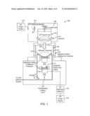
[0014] FIG. 1 is a schematic of a system in accordance with the various embodiments;
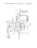
[0015] FIG. 2 is a schematic of the system of FIG. 1 utilizing a diffuser ring;
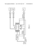
[0016] FIG. 3 shows a modified etching system in accordance with the various embodiments;
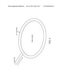
[0017] FIG. 4 shows a ring diffuser with 1 mm holes in accordance with the various embodiments;
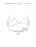
[0018] FIG. 5A is a plot of NF3 flow rate through the ring diffuser versus etch rate for a system in accordance with the various embodiments;
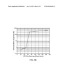
[0019] FIG. 5B is a plot of NF3 flow rate through the ring diffuser versus smoothness for a system in accordance with the various embodiments;
[0020] FIG. 6A is an AFM image of the smoothest substrate obtained with an ring active etch in accordance with the various embodiments;
[0021] FIG. 6B is an SEM image of the etch region cross section for the substrate of FIG. 6A;
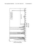
[0022] FIG. 7A shows residual gas analyzer data for two methods, including a method in accordance with the various embodiments; and
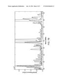
[0023] FIG. 7B shows a detailed view of a portion of the data of FIG. 7A.
DETAILED DESCRIPTION
[0024] The present invention is described with reference to the attached figures, wherein like reference numerals are used throughout the figures to designate similar or equivalent elements. The figures are not drawn to scale and they are provided merely to illustrate the instant invention. Several aspects of the invention are described below with reference to example applications for illustration. It should be understood that numerous specific details, relationships, and methods are set forth to provide a full understanding of the invention. One having ordinary skill in the relevant art, however, will readily recognize that the invention can be practiced without one or more of the specific details or with other methods. In other instances, well-known structures or operations are not shown in detail to avoid obscuring the invention. The present invention is not limited by the illustrated ordering of acts or events, as some acts may occur in different orders and/or concurrently with other acts or events. Furthermore, not all illustrated acts or events are required to implement a methodology in accordance with the present invention.
[0025] The various embodiments are directed to etch apparatus and methods that achieve glass high etch rates, at least in the 1-100 μm/min range, for glass substrates resulting in another order of magnitude improvement in the etch rate of glass.
[0026] In 2004, Yamakawa et al. [19] demonstrated a very high speed etching of silicon dioxide (BPSG) film using microwave excited non-equilibrium atmospheric pressure plasma. The authors were able to demonstrate an ultra-high etch rate of SiO2 (14 μm/min) and an unprecedented selectivity of 200 with respect to silicon using NF3/He along with addition of H2O as the etching gas. In this configuration, the inventors note that the fast etch rate can be attributed to the presence of NFx radicals arising from the breakup of NF3 into NFx*+F*--radicals. NFx--radicals (with x>0). These radicals are extremely aggressive towards SiO2 and other dielectrics (and polymers) and can etch them at extremely high speed. The addition of water vapor (H2O) consumes the fluorine radicals by HF formation (2F*+H2O→2HF+<0>) whereas NFx radicals are much less scavenged. Accordingly, water vapor therefore acts as a selective fluorine radical scavenger and consequently reduces any undesirable attack of silicon. However, if NF3 is completely broken down, e.g., as in high-density, high power plasma, then the plasma primarily consists only of fluorine and nitrogen radicals. Under these conditions, a complete quenching of the fast etch rate of SiO2 and other dielectrics has been observed. The complete breakup of NF3 molecules under appropriate plasma conditions can also confirmed by the plasma color which changes from a deep red to a bluish color, indicating a change in preponderance from NFx to fluorine radicals in the plasma.
[0027] Thus, the inventors note that a main requirement for speeding up glass etch rate requires the creation of NFx radicals. However, to date no reports of such high etch rates in high density plasma sources such as ICP-RIE systems exist. This is mainly due to the fact that these conditions cannot be readily reproduced in an ICP-RIE system. In an ICP-RIE process, the pressure is typically too low (˜1×10⁻³ mbar) and the coupling of high RF power results in a complete breakdown of the NF3 into nitrogen and fluorine radicals. The high density of plasma achieved in ICP chambers results in a very efficient transfer of energy between the RF source and the gas in the chamber and essentially breaks up the molecules into individual atomic radicals and ions. To overcome this limitation and to achieve the incomplete breakup of the NF3 molecules, high chamber pressure is required. However, even if the pressure is increased a 100 times, conventional ICP-RIE processes still cannot achieve the results reported in microwave plasma. Furthermore, at these pressures a high mismatch between the source and chamber load occurs and the typical tuning circuits available on the etching equipment are unable to tune. As a result, any resulting plasma is typically extinguished.
[0028] Although the various embodiments will be described primarily with respect to an ICP system, this is solely for illustrative purposes. That is, the various embodiments are not limited to any particular high density plasma source. For example, the high density plasma can be generated using a magnetically enhanced plasma source, a helicon plasma source, or a capacitively coupled plasma source, to name a few. However, other methods for generating high density or any other source of plasma can be considered as suitable for this application. Thus, an ICP source described below with respect to the various figures can be substituted with any other type of high density or ordinary plasma source.
[0029] Based on the foregoing, the inventors have determined that in order to exploit the most of the ICP-RIE etchers for glass etching the following conditions are required:
[0030] a. Operation of the ICP-RIE etcher under its normal operating pressure and power range to obtain efficient plasma conditions.
[0031] b. Providing for conditions within the chamber to create incomplete breakup of the NF3 molecules to achieve the high etch rate.
[0032] c. Achieving control over the etch rate, etch smoothness, and anisotropy of the structure independently of the plasma source conditions.
[0033] d. Introduction of water molecules into the chamber either through the nozzle or any other means in the proximity of the substrate.
[0034] In view of the foregoing, the various embodiments of the invention are directed to new systems and methods for etching of glass using NF3 gas using ICP-RIE etching. In particular, new systems and method that meet the goals listed above during etching of glass. In the various embodiments, these goals are achieved by incorporating a gas diffuser in the vicinity of the wafer or other material to be etched to provide a localized source of NF3 gas in the ICP-RIE reactor. For example, in one embodiment, a stainless steel gas diffuser ring can be provided on the metal plate on the mechanical clamping plate of the etcher. In particular, the gas diffuser is positioned in the ICP-RIE reactor so that the gas diffuser dispenses NF3 and/or H2O and/or any other gas of interest right above the wafer.
[0035] In operation, the etch process is imitated in a conventional manner. That is, conventional etch process gases are introduced into the ICP-RIE reactor (e.g., Ar, SF6) and a plasma is generated, remote from the wafer, using normal operating conditions. Concurrently, NF3 gas is introduced in the vicinity of the wafer using the gas diffuser. A substrate bias power is applied during this process, which drives the high energy ions generated in the plasma towards the NF3 gas in the vicinity of the wafer. These ions then interact with the NF3 gas to break it down into NFx radicals. Effectively, this creates a high pressure plasma in the vicinity of the wafer inside a low pressure ICP-RIE chamber. This effective high density NF3 plasma with the incomplete breakdown of the gas molecules is then used to achieve a high etch rate of glasses. In particular, etch rates of 1 μm/min range or higher for glass substrates. In other words, etch rates that are at least an order of magnitude than conventional methods.
[0036] In another variation, H2O is introduced in the proximity of the substrates/wafer to enhance the reactivity of the NF3 radicals with the glass substrate. Water molecules can react with the NFx and F radicals and scavenge them to create the right etching mixture. Furthermore, water can also help in wetting the glass surface and initiate and mediate reactions on the surface through the interactions with various radicals and ions thus formed in the chamber.
[0037] Any sequence of gas introduction through the diffuser ring can be considered. For example, alternate introduction of NF3 gas followed by H2O gas, or simultaneous introduction of the two gases, or concurrent introduction using two independent nozzles or diffuser rings. Neither gas is limited to NF3 or H2O only and any gases that contain active species relevant for glass etching can be considered in this arrangement.
[0038] In the various embodiments, the energy of the bombarding ions from the plasma can be effectively controlled by the substrate bias which provides an independent control to change the etching conditions for tuning the composition of the NFx radicals as well as to control the anisotropy. Further, by controlling the plasma gas composition from the gas diffuser, in-situ reactions and gas chemistries in the vicinity of the wafer can be increased or decreased as needed.
[0039] FIG. 1 shows a schematic illustration of an ICP-RIE system 100 in accordance with the various embodiments. The system 100 includes many components of a conventional ICP-RIE system. For example, the system 100 can include a plasma chamber 102, serving as a source of inductively coupled plasma or ICP source. The plasma chamber 102 is coupled to a diffusion chamber 104 lined with magnetic portions 106, in which the wafer to be etched is disposed and into which ions from the ICP source are directed towards the wafer to perform the etching. The plasma chamber 102 can include a gas inlet 108 for introducing gases into the plasma chamber 102. This gas inlet can be coupled to a gas delivery system (not shown) for delivering one or more gases. For example, the gas delivery system can be configured to delivery of SF6, C4F8, Ar, O2, CH4, CHF3, CF4, Cl2, Xe, Ne, N2, or NF3, or any combinations thereof. The plasma chamber 102 can also be associated with an antenna or coil 110, an RF matching or tuning network 112 and an RF power supply 113 to provide the energy for generating the plasma in the plasma chamber 102.
[0040] The diffusion chamber 104 can include a substrate holder and clamp 114 for supporting and securing a wafer. As shown in FIG. 2, the substrate holder 114 can be configured such that the position (i.e., the height) of the wafer in the diffusion chamber can be changed as required to reduce or increase the distance between the plasma chamber 102 and the wafer. During etching, the temperature of the wafer can be controlled using back side Helium cooling lines 116 coupling the substrate holder 108 to a chiller (not shown). The He cooling lines can be configured to allow temperatures between -20-50 ° C. The substrate holder and clamp 114 can be further configured to serve as an electrode coupled to a second RF generator or power supply 116 via a second RF matching/tuning network 115 to provide substrate bias. This second RF generator 116 and second RF matching/tuning network 115 can be configured to be decoupled from and operate independently of the RF generator 113 and RF matching tuning network 112 associated with the plasma chamber 102.
[0041] Although FIG. 1 and other descriptions refer to discrete plasma and diffusion chambers, the various embodiments are not limited in this regard. That is, in some configurations, a single chamber can be provided with different regions to serve as the plasma chamber 102 and the diffusion chamber 104.
[0042] In addition to the foregoing, the system 100 can include a gas diffuser 118 coupled to a gas delivery system (not shown) via feedthroughs 120 for introducing NF3 gas and other gases, separately or in combination, into the diffusion chamber 104 in the vicinity of substrate holder 114 when in the elevated position. Such other gases can include, but are not limited to H2O. In the various embodiments, the gas delivery system for the gas diffuser 118 can be the same or different than the gas delivery system for inlet 108. However, providing a separate gas delivery systems for inlet 108 and gas diffuser 118 can be advantageous. That is, separate systems provide greater flexibility and control. For example, the mixture of gases introduced via inlet 108 and gas diffuser 118 can be different.
[0043] In the various embodiments, the gas diffuser 118 can be implemented in a variety of ways. In some embodiments, as illustrated in FIG. 2, the gas diffuser 118 can be implemented as diffuser ring 218, flexible feedthroughs 220 coupling the diffuser ring 218 to a gas panel 222, and an NF3 gas source 224 coupled to gas panel 222. In one particular embodiment, the diffuser ring 214 can be constructed using a 1/8 inch electro-polished stainless steel tube drilled with 0.5 mm holes at a distance of 10 mm bent into a 4'' circular tube. Thereafter this tube can be welded onto the substrate holder and clamp 108. The tube can be coupled via flexible gas tubing, serving as flexible feedthroughs 220, to the gas panel 222 to permit gas delivery and to account for the different positions of the substrate holder and clamp 108. For example, stainless steel flexible gas tubing using VCR fittings can be used to bring the process gas to the diffuser ring 218. Additionally one or more the flexible feedthroughs 220 can include non-flexible portions or segments 221, as shown in FIG. 3. Further, additional tubing 226 can be provided to connect the various components described above.
[0044] Although the discussion above describes that the gas diffuser 114 is implemented as a diffuser ring, the various embodiments are not limited in this regard. Rather, any other structure can be used in the various embodiments. For example, the gas diffuser 118 can be implemented using individual nozzles disposed in the vicinity of the substrate. In another example, gas diffuser 118 can be implemented using multiple sections of tubing with holes or openings. Further, although the diffuser ring 214 is described as containing holes or openings disposed substantially along a same plane parallel to that of the wafer, having a particular size, and having a particular spacing, the various embodiments are not limited in this regard. Rather, a gas diffuser in accordance with the various embodiments can provide any placement, spacing, size, or other arrangement of holes or openings for introducing gases into diffusion chamber 104. Similarly, other configurations of gas diffuser 118 can be configured with a wide array of geometries.
[0045] The gas panel 222 can also be configured in a variety of ways. In one particular embodiment, a precision needle valve can be used to control the gas flow rate of NF3 (or other gases) into the diffusion chamber 104. In one particular embodiment, a NF3 flow rate of 300 sccm or less can be used. However, any other methods for controlling gas flow rate can be used in the various embodiments.
[0046] In one particular embodiment, a precision needle valve can be used to control the gas flow rate of H2O (or other gases) into the diffusion chamber 104. In one particular embodiment, a H2O flow rate of 300 sccm or less can be used. However, the flow rates and methods for controlling gas flow rate can vary in the various embodiments. In addition to the foregoing, the system 100 can include additional modifications compared to conventional ICP-RIE systems. For example, plasma shielding plates may need to be modified to accommodate the additional components for the system 100. In some embodiments, the system 100 can also be coupled to a mass-spectrometer system (e.g., a residual gas analyzer) to measure the gas species created within the chamber to monitor and adjust the etching process. Additionally, optical windows can be provided to monitor the visible/UV spectra of the plasma and evaluate the plasma glow composition during etching.
[0047] The modifications described above allow an ICP-RIE reactor in accordance with the various embodiments to be used in a variety of modes. A first mode of operation is simply to utilize the ICP-RIE reactor to perform etching under normal operating conditions. That is, to perform conventional (i.e., low etch rate) etch processes. For such normal operations, the plasma etching occurs by generating a plasma using an etching gas chemistry (e.g., NF3 and Ar) without introducing gases through the gas diffuser. That is, referring back to FIG. 1, gases are introduced view inlet 108 and a plasma 130 is generated in plasma chamber 102. Concurrently, a substrate bias is provided at substrate holder and clamp 114, which causes ions generated in the plasma 130 to be directed towards substrate holder and clamp 114 and any wafer disposed thereon. The ions are then used to perform conventional etching. Such a mode can be utilized when low etch rates are desirable to accurately.
[0048] A second mode is to utilize the gas diffuser to generate enhanced etching conditions. In such a mode, the system can be initially setup in the first mode, as described above. Thereafter, the etch gas (NF3) can be introduced into the ICP-RIE reactor via the gas diffuser and the enhanced etching (high etch rate) will be performed. That is, as described above, the plasma 130 is generated and the substrate bias is used to direct ions from the plasma 130 towards the wafer. However, via gas diffuser 118, a region 132 with an increased density of NF3 gas, localized around the wafer, is provided. The interaction of the ions from the plasma 130 with the NF3 132 in region 132 causes the generation of NFx radicals. That is, the ions are utilized to break up the NF3 in region 132 to provide the incomplete breakup of NF3. This results in effectively forming a high density plasma of NFx radicals in the vicinity of the wafer. Consequently, the presence of a high concentration of these NFx radicals enhances the etch rate.
[0049] Although the various embodiments are described with respect to the enhanced etching of glasses using a NF3-based chemistry in an ICP-RIE reactor modified to include a gas diffuser, the various embodiments are not limited in this regard. Rather, the systems and methods described herein can be applied to the etching of any other types of materials and using other types of chemistries.
EXAMPLES
[0050] The following examples and results are presented solely for illustrating the various embodiments and are not intended to limit the various embodiments in any way.
[0051] Smooth dry etching of some types of borosilicate glass wafers has been a challenge due to nonvolatile or less volatile metal-halogen compounds forming on the surface of the etched area. Thus, the methods of the various embodiments have been evaluated. In particular, to evaluate the methods of the various embodiments, two alternative etching method were investigated in regards of smooth and fast etching; i) Conventional Ar/NF3 downstream plasma etching ii) Ar/O2/NF3 plasma etching where an inductively coupled plasma reactor is modified such that a ring shape diffuser system is adapted to the substrate holder in order to supply high local etchant flux, NF3, over the substrate surface. The latter approach, in accordance with the various embodiments, reduces the full dissociation of NF3 in NF3/AR and O2 based plasma and resulted in forming more reactive species in the plasma RGA (Residual gas analysis) show that the diffuser system allows to form larger amounts of NFx radicals in the plasma. Further, ex-situ X-ray Photoelectron Studies (XPS) showed non-volatile metal alkali compounds are formed on the surface on rough surfaces, with NaF being the prominent compound for the Schott Borofloat glass. For smooth surfaces, less alkali compounds are observed. The results demonstrated that ultra-smooth etch surfaces can be obtained within a window of parameters, where the arithmetic mean smoothness (Ra) varies from 3.4 Å to 8 Å at considerable etch rates of 0.343 μm/min to 0.55 μm/min.
[0052] I. Introduction
[0053] One of the most important and challenging parameters in micromachining of Borofloat glass is obtaining smooth surfaces at considerable etch rates [13]. Despite the fact that, controlled surface roughness is shown to be useful for some specific applications [14], surface roughness in general is highly unwanted in most of the applications such as optical applications and micro-electro-mechanical systems (MEMS) [15]. If the surface is rough and wavy, the light is scattered in optical applications. Therefore, high precision optical applications require close to atomically flat surface roughness (Ra˜0.5-1 nm). For micro machined resonators and sensors, roughness negatively affects the quality factor and thus decreases the fabricated device performance. The causes of increased roughness are due to the impurities exist in glass substrates and due to the less percent metal containing compounds other than SiO2, where these metal based compounds form non-volatile or less volatile metal halogens in fluorine containing plasmas (i.e., Argon/SF6) during dry etching. For instance, Borosilicate glass, is mainly composed of 81% of SiO2, 13% of B2O3, 4% of Na2O/K2O and 2% of Al2O3. The non-volatile metal/alkali metal halogens (i.e., NaF and AlF3) forming on the surface cause micro-masking in the etch regions resulting in the formation of needle-like structures and therefore destructing the smoothness. As a solution, highly energetic argon ions are proposed as the physical etch mechanism to remove these compounds from the surface to achieve better roughness, but as the argon percent ratio in the gas mixture is increased, the etch rate decreases significantly [16]. Furthermore, the arithmetic mean roughness (Ra) is still reported on the range of 2 nm to 100 nm in these cases [16]-[19].
[0054] II. Etching mechanism
[0055] In this study, an etching system in accordance with the various embodiments was utilized in order to achieve smoothness at considerable etch rates. A radio frequency (RF) inductively coupled plasma etching system (Alcatel AMS 100, manufactured by Alcatel-Lucent of Paris, France) is modified, where a ring diffuser mechanism is attached to the substrate holder. The whole system and the ring are shown in FIGS. 3 and 4. FIG. 3 shows a modified etching system in accordance with the various embodiments and FIG. 4 shows a ring diffuser with 1 mm holes in accordance with the various embodiments. The ring has a diameter of 9.6 cm and has diffuser holes that are placed within 1 mm spacing.
[0056] In most of the ICP applications and in the case of unmodified etching system chemical and physical etchants are introduced via the gas inlets located at the top of the ICP chamber [20]. The plasma is formed within this chamber and directed towards the substrate in a downstream fashion via the applied electric field between the source and the substrate. The main purpose of the ring diffuser proposed here is to enhance the reactive ion etching via establishing high local flux of reactive species on etch face of the wafer, combining the downstream flux with the local ring flux. Before characterizing the effect of ring design on smoothness, etch rate and hard mask selectivity over substrate, classical downstream etches using Ar and NF3, where the ring is inactive, are performed in sake of determining the etch performance. A set of experiments utilizing design of experiments involving orthogonal arrays are carried out to obtain optimum conventional ring-inactive downstream etching parameters using Ar/NF3 plasma (Please refer to the supplemental information for the detailed experimentation). Double-side polished, 4 inches Borosilicate wafers are used as the substrates during all experiments performed. The wafers are patterned with 100 um, 250 um, 500 um and 1 mm rectangular openings. 2-3 um thick nickel is plated on the wafers, acting as hard mask during the etch. Each sample is etched for 1 hour at 20° C. substrate temperature. The results for fastest and smoothest Ar/NF3 etches are demonstrated in Table 1.
TABLE-US-00001 TABLE 1 Baseline results for AR/NF3 conventional ICP plasma. ICP Substrate Stage Ar flow NF3 flow Smoothness power Power position Pressure rate rate Etch rate (Ra) Fastest 2000 W 400 W 120 mm 6.5 × 10⁻⁶ bar 10 sccm 30 sccm 0.41 μm/min 79.6 nm Smoothest 2000 W 400 W 120 mm 12 × 10-6 bar 30 sccm 12.5 sccm 0.31 μm/min 28.1 nm
Summarized results from Table 1 are taken into consideration to start experimental design of the ring active experiments. For the ring-active experiments, 20 sccm of Ar and 10 sccm of O2 are introduced from top into the ICP chamber. The ICP power, substrate power and the stage position are all held constant with the ones stated in Table 1. The pressure is not regulated. Various flow rates of NF3 are feed through the ring diffuser. FIGS. 5A and 5B shows the etch rate and recorded operating pressure along with the smoothness in the chamber when the ring is active. The etch depths are measured via a Tencor P16+ profilometer, manufactured by KLA Tencor of Milpitas, Calif. and the roughness is measured via a PSIA XE-100 Scanning Probe Microscope, manufactured by Park Systems Corporation of Santa Clara, Calif.
[0057] As the ring is utilized and the NF3 flow is kept between 20-50 sccm, high etch rates and ultrasmooth surfaces are obtained. The maximum etch rate, 0.55 μm/min, is achieved at 20 sccm Ar/10 sccm O2/48 sccm NF3 flows. The best smoothness, Ra=3.4 Å, is achieved at 20 sccm flow, where the wall slope was 82.4°. An Atomic Force microscope (AFM) image and an scanning electron microscope (SEM) image of the substrate are shown in FIGS. 6A and 6B, respectively. The obtained smooth substrates can be readily used for optical applications involving high precision (Ra<5 Å) and super precision (Ra<3 Å). Even at the highest etch rate, Ra is measured as 8.4 Å. However, the smoothness is heavily degraded once the ring flow rate is above 50 sccm. In this case, Ra is at least 2 orders of magnitude larger in high flow regions where the chamber pressure is >6.3 μBar.
[0058] When compared to conventional downstream etching with Ar/NF3 , where the results are tabulated in Table 1, the etch rate with the ring is improved 34%. The nickel selectivity at downstream Ar/NF3 plasma is measured as 7.35:1 over Borosilicate glass. In ring active experiments of FIGS. 4A and 4B, the selectivity is measured as 9.32:1 for the fastest etch rate, indicating a 27% improvement.
[0059] The superior performance of one etching method among two etching methods is mainly due to the diffuser mechanism. The aim to have diffuser mechanism in place is to decrease the dissociation rate of NF3 and obtain more NFx radicals in tha plasma. It is previously stated that the low percent dissociation of NF3 improves the etching speed of borosilicate glass [21]. In order to determine the gas species forming in the plasma, a Residual Gas Analyzer (Exton XT 100, manufactured by Extorr, Inc. of New Kensington, Pa.) is used. FIGS. 7A and 7B show two RGA data: for the ring active etch at 48 sccm NF3 flow rate and for Ar/NF3 plasma with fastest etch rate shown in Table 1. From FIGS. 7A and 7B, it is clearly observed that the plasma creates considerable partial pressure of NFx (NF.sup.+ and NF2.sup.+ at the peaks 33 and 52 respectively) radicals in the plasma. In addition, NF3 at peak 71 has considerable partial pressure. However, in conventional Ar/NF3 plasma, there is no peak at NF3, proving a full dissociation in the gas. There are less NF2 and NF radicals, indicating NF3 dissociated mostly to N and F. The highly energetic Argon ions, which is accelerating towards the wafer surface first interacts with a local flux of NF3 gas that is just over the substrate. The collisions between Argon and NF3 create high concentrations of NFx. NFx radicals may act more aggressive to glass and thus improve the etch rate. In addition, heavier gasses are formed when the ring is active. The peak 84 may highly correspond to NF2O2 gas. The authors articulate there may be NFxOx based gas formation when NF3 is diffused through the ring, which may be playing a critical role in smoothness and fast etching. This is further discussed in below.
[0060] As it is pointed out above, smoother surfaces are obtained via the diffuser system. In order to understand the smoothness achievement further and to determine the surface chemistry by estimating the atomic composition of the surfaces, X-ray Photoelectron Spectroscopy (XPS) is used. Three etching results are compared in XPS study: i) the fastest etch obtained in Ar/NF3 etching system shown in table 1 ii) Ring active etch with 20 sccm NF3 flow iii) Ring active etch with 80 sccm flow. All these have 79.6 nm, 0.34 nm and 350 nm of Ra respectively. These 3 runs are selected to compare two different etching methods and determine the effect of ring diffuser system on roughness. As previous studies in literature indicate, the non-volatile species negatively affect the smoothness. Not only the smoothness is lost by these species, but the etch rate also decreases (the degree of decrease depending on the composition of the glass type) as the non-volatile species concentration/accumulation on the substrate surface increases during the etching [22]. Therefore, high resolution XPS scans have been performed for Sodium (Na), Boron (B), Aluminum (Al) and Potassium (K). Table 2 shows the atomic percent calculations of 3 etching results emphasized.
TABLE-US-00002 TABLE 2 Approximate atomic percent calculations from XPS surveys for 3 different etch cases comparing two etching approach. All values are in percent. Si 2s O 1s F 1s Na 1s B 1s Al 2s K 2s Ni 2p Ar/NF3 fastest etch 4.01 8.979 57.76 18.56 ND* 7.646 1.279 1.768 Ring active etch- 20 sccm 20.7 51.696 15.751 7.526 2.105 2.22 ND* ND* NF3 Ring active etch- 80 sccm 4.483 6.487 56.448 20.946 4.144 5.102 1.887 ND* NF3 Unprocessed wafer 27.91 66.92 ND* 0.46 4.69 ND* ND* ND* *ND: Not Detectable amount.
[0061] From approximate atomic percent calculations, it is observed that the rough samples have high Al, K and Na percentage. However, it is interesting to note that Na is the most prominent amongst them. For the conventional Ar/NF3 etching and high flow ring active etching have very high Na concentrations (>15%) at the surface, whereas smooth ring active etch has 7.5% Na concentration. When Ra roughness is considered, this much of difference in Na percentages causes 2 orders of magnitude worse roughness. These results infer that the smoothness is enhanced via ion enhanced chemical reaction introduced by the ring diffuser system.
[0062] In conclusion, a system configured in accordance with the various embodiments can be used to obtain smooth surfaces on borosilicate glass and is integrated with a commercial ICP etching system, where NF3 is supplied to the diffuser. The effects of the mechanism are compared with conventional Ar/NF3 plasma etching. Ultra-smooth etching is achieved with Ra<5 Å at considerable etch rates. The smoothness is degraded at high flows of NF3 (>50 sccm). The main reason of this degradation is due to the high percentages of Na (in NaF form) on the surface. At smooth etches, the Na concentration is found out to be less in atomic percent. The authors articulate that higher amount of NFx radicals and possible existence NFxOx gasses effectively remove Na from the surface in the light of RGA readouts.
[0063] While various embodiments of the present invention have been described above, it should be understood that they have been presented by way of example only, and not limitation. Numerous changes to the disclosed embodiments can be made in accordance with the disclosure herein without departing from the spirit or scope of the invention. Thus, the breadth and scope of the present invention should not be limited by any of the above described embodiments. Rather, the scope of the invention should be defined in accordance with the following claims and their equivalents.
[0064] Although the invention has been illustrated and described with respect to one or more implementations, equivalent alterations and modifications will occur to others skilled in the art upon the reading and understanding of this specification and the annexed drawings. In addition, while a particular feature of the invention may have been disclosed with respect to only one of several implementations, such feature may be combined with one or more other features of the other implementations as may be desired and advantageous for any given or particular application.
[0065] The terminology used herein is for the purpose of describing particular embodiments only and is not intended to be limiting of the invention. As used herein, the singular forms "a", "an" and "the" are intended to include the plural forms as well, unless the context clearly indicates otherwise. Furthermore, to the extent that the terms "including", "includes", "having", "has", "with", or variants thereof are used in either the detailed description and/or the claims, such terms are intended to be inclusive in a manner similar to the term "comprising."
[0066] Unless otherwise defined, all terms (including technical and scientific terms) used herein have the same meaning as commonly understood by one of ordinary skill in the art to which this invention belongs. It will be further understood that terms, such as those defined in commonly used dictionaries, should be interpreted as having a meaning that is consistent with their meaning in the context of the relevant art and will not be interpreted in an idealized or overly formal sense unless expressly so defined herein.
REFERENCES
[0067] The following references describe concepts associated with various aspects of the invention and are each incorporated by reference in their entirety:
[0068] [1] L. Li, T. Abe, and M. Esashi, Journal of Vacuum Science & Technology B (Microelectronics and Nanometer Structures), vol. 21, p. 2545, 2003.
[0069] [2] X. Li, T. Abe, and M. Esashi, Proceedings of IEEE Thirteenth Annual International Conference on Micro Electro Mechanical Systems, Miyazaki, Japan, 2000, p. 271.
[0070] [3] A. Goyal, V. Hood, and S. Tadigadapa, Journal of Non-Crystalline Solids, vol. 352, p. 657, 2006.
[0071] [4] S. Queste, R. Salut, S. Clatot, J.-Y. Rauch, G. Chantal, and M. Khan, Microsystems Technology, vol. 16, pp. 1485-1493, 2010.
[0072] [5] S. Karecki, R. Chatterjee, L. Pruette, R. Reif, T. Sparks, L. Beu, V. Vartanian, and K. Novoselov, Journal of the Electrochemical Society, vol. 148, pp. 141-9, 2001/03/2001.
[0073] [6] S. S. Choi, D. W. Kim, and M. J. Park, Journal of the Korean Physical Society, vol. 45, pp. 1500-1504, December 2004.
[0074] [7] C.-H. Yang and C.-M. Dai, Proceedings of the SPIE--The International Society for Optical Engineering Optical Microlithography XI, 25-27 Feb. 1998, vol. 3334, pp. 553-8, 1998//1998.
[0075] [8] F. H. Bell, O. Joubert, G. S. Oehrlein, Y. Zhang, and D. Vender, Journal of Vacuum Science & Technology A (Vacuum, Surfaces, and Films), vol. 12, pp. 3095-101, 1994/11/1994.
[0076] [9] G. Adegboyega, I. PerezQuintana, A. Poggi, E. Susi, and M. Merli, Journal of Vacuum Science & Technology B, vol. 15, pp. 623-628, May-June 1997.
[0077] [10] B. A. Cruden, M. V. V. S. Rao, S. P. Sharma, and M. Meyyappan, Journal of Vacuum Science & Technology B (Microelectronics and Nanometer Structures), vol. 20, pp. 353-63, 2002/01/2002.
[0078] [11] A. Nagy, Optical Engineering, vol. 31, pp. 335-340, February 1992.
[0079] [12] C. H. Lin, G. B. Lee, Y. H. Lin, and G. L. Chang, Journal of Micromechanics and Microengineering, vol. 11, pp. 726-732, November 2001.
[0080] [13] Xinghua Li, Takashi Abe, and Masayoshi Esashi, Sensors and Actuators A: Physical 87 (3), 139 (2001).
[0081] [14] E. Hein, D. Fox, and H. Fouckhardt, Journal of Applied Physics 107 (3), 033301 (2010).
[0082] [15] A. M. Hynes, H. Ashraf, J. K. Bhardwaj, J. Hopkins, I. Johnston, and J. N. Shepherd, Sensors and Actuators A: Physical 74 (1-3), 13 (1999); Lee A. Donohue, Janet Hopkins, Richard Barnett, Andrew Newton, and Anthony Barker, 44 (2004).
[0083] [16] T. Ichiki, Y. Sugiyama, R. Taura, T. Koidesawa, and Y. Horiike, Thin Solid Films 435 (1), 62 (2003).
[0084] [17] D. A. Zeze, R. D. Forrest, J. D. Carey, D. C. Cox, I. D. Robertson, B. L. Weiss, and S. R. P. Silva, Journal of Applied Physics 92 (7), 3624 (2002).
[0085] [18] S. Queste, R. Salut, S. Clatot, J. Y. Rauch, and ChantalG Khan Malek, Microsystem Technologies 16 (8-9), 1485 (2010).
[0086] [19] Abhijat Goyal, Vincent Hood, and Srinivas Tadigadapa, 61110P (2006).
[0087] [20] H. Sugai, K. Nakamura, Y. Hikosaka, and M. Nakamura, Journal of Vacuum Science & Technology A: Vacuum, Surfaces, and Films 13 (3), 887 (1995).
[0088] [21] Koji Yamakawa, Masaru Hori, Toshio Goto, Shoji Den, Toshirou Katagiri, and Hiroyuki Kano, Applied Physics Letters 85 (4), 549 (2004).
[0089] [22] EzzEldin Metwalli and Carlo G. Pantano, Nuclear Instruments and Methods in Physics Research Section B: Beam Interactions with Materials and Atoms 207 (1), 21 (2003).
User Contributions:
Comment about this patent or add new information about this topic:
| People who visited this patent also read: | |
| Patent application number | Title |
|---|---|
| 20140165354 | VEHICLE BATTERY UNIT INSTALLATION APPARATUS |
| 20140165353 | CRIMPING TOOL |
| 20140165351 | Burnishing Device and Burnishing Method Using It |
| 20140165350 | MACHINE AND METHOD FOR BEDDING BRAKE PADS AND DISCS |
| 20140165348 | MACHINE TOOL WITH LATHE TOOL AND MILLING CUTTER |

