Patent application title: SHIFT REGISTER
Inventors:
Shih-Song Cheng (Hsin-Chu, TW)
Chun-Yen Liu (Hsin-Chu, TW)
Chun-Yen Liu (Hsin-Chu, TW)
Assignees:
AU OPTRONICS CORP.
IPC8 Class: AG11C1918FI
USPC Class:
377 68
Class name: Electrical pulse counters, pulse dividers, or shift registers: circuits and systems shift register compensating for or preventing signal deterioration
Publication date: 2014-05-22
Patent application number: 20140140468
Abstract:
A shift register includes a previous signal receiving unit, a next signal
receiving unit, a control unit and a voltage stabilizing switch. The
shift register controls an outputting signal by continuously stabilized
voltage generated from cooperating operation of the units and switch.Claims:
1. A shift register, comprising: a previous signal receiving unit,
comprising a previous signal input terminal, a previous first
preset-voltage input terminal, a previous second preset-voltage input
terminal, a previous first control-signal output terminal, and a previous
second control-signal output terminal, wherein the previous signal input
terminal receives a previous signal, the previous first preset-voltage
input terminal is electrically coupled to a first preset-voltage source,
the previous second preset-voltage input terminal is electrically coupled
to a second preset-voltage source, and the previous signal receiving unit
controls degrees of an electrical conduction between the previous first
preset-voltage input terminal and the previous first control-signal
output terminal according to a voltage of the previous signal, and
controls degrees of an electrical conduction between the previous second
preset-voltage input terminal and the previous second control-signal
output terminal according to the voltage of the previous signal; a next
signal receiving unit, comprising a next signal input terminal, a next
second preset-voltage input terminal, and a next control-signal output
terminal, wherein the next signal input terminal receives a next signal,
the next second preset-voltage input terminal is electrically coupled to
the second preset-voltage source, the next control-signal output terminal
is electrically coupled to the previous first control-signal output
terminal, and the next signal receiving unit controls degrees of an
electrical conduction between the next second preset-voltage input
terminal and the next control-signal output terminal according to a
voltage of the next signal; a control unit, comprising a first
preset-voltage input terminal, a clock-signal input terminal, a reversed
clock-signal input terminal, a first control-signal input terminal, a
second control-signal input terminal, and an output terminal, wherein the
first preset-voltage input terminal is electrically coupled to the first
preset voltage source, the clock-signal input terminal receives a clock
signal, the reversed clock-signal input terminal receives a reversed
clock signal having a phase reversed to that of the clock signal, the
first control-signal input terminal is electrically coupled to the
previous first control-signal output terminal, the second control-signal
input terminal is electrically coupled to the previous second
control-signal output terminal, and the control unit controls degrees of
an electrical conduction between the clock-signal input terminal and the
output terminal according to voltages of the reversed clock-signal input
terminal, the first control-signal input terminal and the second
control-signal input terminal; and a voltage stabilizing switch,
comprising a control terminal, a first source/drain terminal and a second
source/drain terminal, wherein the control terminal is electrically
coupled to the output terminal of the control unit, the first
source/drain terminal is electrically coupled to the previous first
control-signal output terminal, and the second source/drain terminal is
electrically coupled to the previous first preset-voltage input terminal
of the previous signal receiving unit.
2. The shift register as claimed in claim 1, wherein the previous signal receiving unit comprising: a first transistor, comprising a control terminal, a first source/drain terminal and a second source/drain terminal, wherein the control terminal thereof is electrically coupled to the previous signal input terminal, the first source/drain terminal thereof is electrically coupled to the previous first control-signal output terminal, and the second source/drain terminal thereof is electrically coupled to the previous first preset-voltage input terminal; and a second transistor, comprising a control terminal, a first source/drain terminal and a second source/drain terminal, wherein the control terminal thereof is electrically coupled to the previous signal input terminal, the first source/drain terminal thereof is electrically coupled to the previous second preset-voltage input terminal, and the second source/drain terminal thereof is electrically coupled to the previous second control-signal output terminal.
3. The shift register as claimed in claim 1, wherein the next signal receiving unit comprising: a transistor, comprising a control terminal, a first source/drain terminal and a second source/drain terminal, wherein the control terminal thereof is electrically coupled to the next signal input terminal, the first source/drain terminal thereof is electrically coupled to the next second preset-voltage input terminal, and the second source/drain terminal thereof is electrically coupled to the next control-signal output terminal; and a capacitor, one terminal thereof is electrically coupled to the next second preset-voltage input terminal, and the other terminal thereof is electrically coupled to the next control-signal output terminal.
4. The shift register as claimed in claim 1, wherein the control unit comprising: a first transistor, comprising a control terminal, a first source/drain terminal and a second source/drain terminal, wherein the control terminal thereof is electrically coupled to the second control-signal input terminal, the first source/drain terminal thereof is electrically coupled to the timing-signal input terminal, and the second source/drain terminal thereof is electrically coupled to the output terminal; a second transistor, comprising a control terminal, a first source/drain terminal and a second source/drain terminal, wherein the control terminal thereof is electrically coupled to the first control-signal input terminal, the first source/drain terminal thereof is electrically coupled to the second control-signal input terminal, and the second source/drain terminal thereof is electrically coupled to the first preset-voltage input terminal; a third transistor, comprising a control terminal, a first source/drain terminal and a second source/drain terminal, wherein the control terminal thereof is electrically coupled to the first control-signal input terminal, the first source/drain terminal thereof is electrically coupled to the output terminal, and the second source/drain terminal thereof is electrically coupled to the first preset-voltage input terminal; a fourth transistor, comprising a control terminal, a first source/drain terminal and a second source/drain terminal, wherein the control terminal thereof is electrically coupled to the reversed timing-signal input terminal, the first source/drain terminal thereof is electrically coupled to the output terminal, and the second source/drain terminal thereof is electrically coupled to the first preset-voltage input terminal; and a capacitor, one terminal thereof is electrically coupled to the output terminal, and the other terminal thereof is electrically coupled to the second control-signal input terminal.
5. The shift register as claimed in claim 1, further comprising: a first transistor, comprising a control terminal, a first source/drain terminal and a second source/drain terminal, wherein the control terminal thereof receives the previous signal, the first source/drain terminal thereof is electrically coupled to the previous first preset-voltage input terminal of the previous signal receiving unit, and the second source/drain terminal thereof is electrically coupled to the first preset-voltage source; a second transistor, comprising a control terminal, a first source/drain terminal and a second source/drain terminal, wherein the control terminal thereof is electrically coupled to the output terminal of the control unit, the first source/drain terminal thereof is electrically coupled to the previous first preset-voltage input terminal of the previous signal receiving unit, and the second source/drain terminal thereof is electrically coupled to the first preset-voltage source; and a third transistor, comprising a control terminal, a first source/drain terminal and a second source/drain terminal, wherein the control terminal thereof is electrically coupled to the previous first control-signal output terminal of the previous signal receiving unit, the first source/drain terminal thereof is electrically coupled to the second preset-voltage source, and the second source/drain terminal thereof is electrically coupled to the previous first preset-voltage input terminal of the previous signal receiving unit.
6. The shift register as claimed in claim 1, further comprising: a driving-signal generating module, providing a first driving signal, wherein a phase of the first driving signal is reverse to a phase of a second driving signal composed by a voltage outputted from the output terminal of the control unit; and a driving module, comprising a first input terminal, a second input terminal, a driving module first preset-voltage input terminal, a driving module second preset-voltage input terminal, an enable-signal input terminal, and a driving-signal output terminal, wherein the first input terminal is electrically coupled to the driving-signal generating module to receive the first driving signal, the second input terminal is electrically coupled to the output terminal of the control unit to receive the second driving signal, and the driving module controls degrees of an electrical conduction between the driving module first preset-voltage input terminal and the driving-signal output terminal according to the first driving signal, and controls degrees of an electrical conduction between the enable-signal input terminal and the driving-signal output terminal according to the second driving signal.
7. The shift register as claimed in claim 6, wherein the driving-signal generating module comprising: a first transistor, comprising a control terminal, a first source/drain terminal and a second source/drain terminal, wherein the control terminal thereof is electrically coupled to the previous first control-signal output terminal of the previous signal receiving unit, the first source/drain terminal thereof is electrically coupled to the first input terminal of the driving module, and the second source/drain terminal thereof is electrically coupled to the second preset-voltage source; and a second transistor, comprising a control terminal, a first source/drain terminal and a second source/drain terminal, wherein the control terminal thereof is electrically coupled to the previous second control-signal output terminal of the previous signal receiving unit, the first source/drain terminal thereof receives the reversed clock signal, and the second source/drain terminal thereof is electrically coupled to the first input terminal of the driving module.
8. The shift register as claimed in claim 6, wherein the driving module comprising: a first transistor, comprising a control terminal, a first source/drain terminal and a second source/drain terminal, wherein the control terminal thereof is electrically coupled to the first input terminal, the first source/drain terminal thereof is electrically coupled to the driving-signal output terminal, and the second source/drain terminal thereof is electrically coupled to the first preset-voltage source; a second transistor, comprising a control terminal, a first source/drain terminal and a second source/drain terminal, wherein the control terminal thereof is electrically coupled to the first input terminal, and the first source/drain terminal thereof is electrically coupled to the first preset-voltage source; a third transistor, comprising a control terminal, a first source/drain terminal and a second source/drain terminal, wherein the control terminal thereof is electrically coupled to the second input terminal, the first source/drain terminal thereof is electrically coupled to the second preset-voltage source, and the second source/drain terminal thereof is electrically coupled to the second source/drain terminal of the second transistor; a fourth transistor, comprising a control terminal, a first source/drain terminal and a second source/drain terminal, wherein the control terminal thereof is electrically coupled to the second source/drain terminal of the third transistor, the first source/drain terminal thereof is electrically coupled to the enable-signal input terminal, and the second source/drain terminal thereof is electrically coupled to the driving-signal output terminal; and a capacitor, one terminal thereof is electrically coupled to the driving-signal output terminal, and the other terminal thereof is electrically coupled to the second source/drain terminal of the second transistor.
9. The shift register of claim 1, further comprising: an illuminating signal generating unit with an illuminating control-signal output terminal to output an illuminating control signal, comprising: a first transistor, comprising a control terminal, a first source/drain terminal and a second source/drain terminal, wherein the control terminal thereof is electrically coupled to the previous second control-signal output terminal of the previous signal receiving unit, and the first source/drain terminal thereof is electrically coupled to the first preset-voltage source; a second transistor, comprising a control terminal, a first source/drain terminal and a second source/drain terminal, wherein the control terminal thereof is electrically coupled to the previous second control-signal output terminal of the previous signal receiving unit, and the first source/drain terminal thereof is electrically coupled to the first preset-voltage source; a third transistor, comprising a control terminal, a first source/drain terminal and a second source/drain terminal, wherein the control terminal thereof is electrically coupled to the previous second control-signal output terminal of the previous signal receiving unit, the first source/drain terminal thereof is electrically coupled to the first preset-voltage source, and the second source/drain terminal thereof is electrically coupled to the illuminating control-signal output terminal; a fourth transistor, comprising a control terminal, a first source/drain terminal and a second source/drain terminal, wherein the control terminal thereof is electrically coupled to the previous first control-signal output terminal of the previous signal receiving unit, the first source/drain terminal thereof is electrically coupled to the second preset-voltage source, and the second source/drain terminal thereof is electrically coupled to the second source/drain terminal of the first transistor; a fifth transistor, comprising a control terminal, a first source/drain terminal and a second source/drain terminal, wherein the control terminal thereof is electrically coupled to the second source/drain terminal of the second transistor, and the first source/drain terminal thereof is electrically coupled to the second source/drain terminal of the first transistor; a sixth transistor, comprising a control terminal, a first source/drain terminal and a second source/drain terminal, wherein the control terminal thereof is electrically coupled to the second source/drain terminal of the second transistor, the first source/drain terminal thereof is electrically coupled to the illuminating control-signal output terminal, and the second source/drain terminal thereof is electrically coupled to the second preset-voltage source; a seventh transistor, comprising a control terminal, a first source/drain terminal and a second source/drain terminal, wherein the control terminal thereof receives the clock signal, the first source/drain terminal thereof is electrically coupled to the second source/drain terminal of the fifth transistor, and the second source/drain terminal thereof is electrically coupled to the second preset-voltage source; an eighth transistor, comprising a control terminal, a first source/drain terminal and a second source/drain terminal, wherein the control terminal thereof receives the next signal receiving, the first source/drain terminal thereof is electrically coupled to the second source/drain terminal of the second transistor, and the second source/drain terminal thereof is electrically coupled to the second preset-voltage source; a capacitor, one terminal thereof is electrically coupled to the second source/drain terminal of the second transistor, and the other terminal thereof is electrically coupled to the second source/drain terminal of the fifth transistor.
10. A shift register, comprising: a driving-signal generating module, providing a first driving signal and a second driving signal, wherein a phase of the first driving signal is reverse to a phase of the second driving signal; and a driving module, comprising a first input terminal, a second input terminal, a driving module first preset-voltage input terminal, a driving module second preset-voltage input terminal, an enable-signal input terminal, and a driving-signal output terminal, wherein the driving module is electrically coupled to the driving-signal generating module to receive the first driving signal via the first input terminal and receive the second driving signal via the second input terminal, and the driving module controls degrees of an electrical conduction between the driving module first preset-voltage input terminal and the driving-signal output terminal according to the first driving signal, and controls degrees of an electrical conduction between the enable-signal input terminal and the driving-signal output terminal according to the second driving signal; wherein an enabled duration of the enable-signal input terminal determines an enabled duration of the driving-signal output terminal.
11. The shift register as claimed in claim 10, wherein the driving module comprising: a first transistor, comprising a control terminal, a first source/drain terminal and a second source/drain terminal, wherein the control terminal thereof is electrically coupled to the first input terminal, the first source/drain terminal thereof is electrically coupled to the driving-signal output terminal, and the second source/drain terminal thereof is electrically coupled to the first preset-voltage source; a second transistor, comprising a control terminal, a first source/drain terminal and a second source/drain terminal, wherein the control terminal thereof is electrically coupled to the first input terminal, and the first source/drain terminal thereof is electrically coupled to the first preset-voltage source; a third transistor, comprising a control terminal, a first source/drain terminal and a second source/drain terminal, wherein the control terminal thereof is electrically coupled to the second input terminal, the first source/drain terminal thereof is electrically coupled to the second preset-voltage source, and the second source/drain terminal thereof is electrically coupled to the second source/drain terminal of the second transistor; a fourth transistor, comprising a control terminal, a first source/drain terminal and a second source/drain terminal, wherein the control terminal thereof is electrically coupled to the second source/drain terminal of the third transistor, the first source/drain terminal thereof is electrically coupled to the enable-signal input terminal, and the second source/drain terminal thereof is electrically coupled to the driving-signal output terminal; and a capacitor, one terminal thereof is electrically coupled to the driving-signal output terminal, and the other terminal thereof is electrically coupled to the second source/drain terminal of the second transistor.
Description:
FIELD OF THE INVENTION
[0001] The present invention relates to a shift register, and more particularly to a shift register with stabilized outputted control voltages.
BACKGROUND OF THE INVENTION
[0002] A shift register is a kind of electronic component, which is widely used and seen in many electronic products. Generally, plural shift-register stages are connected one by one in series to form a shift register group, and an electronic signal is transmitted from a previous shift register to a next shift register stage. Therefore, the electronic signal can achieve correctly function at different locations in different time due to a delay time of a signal transmission in the shift register group.
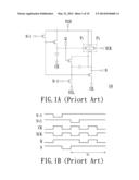
[0003] Referring to FIG. 1A and FIG. 1B, FIG. 1A is a circuit diagram of a typical shift register, and FIG. 1B is a waveform diagram of signals respectively corresponding to each node in the shift register. Shown as in FIG. 1A and FIG. 1B, the shift register 10 receives an output signal N-1 from (N-1)th shift register, an output signal N+1 from (N+1)th shift register, a clock signal CK, a reversed clock signal XCK, etc. as control signals of the shift register 10. Output voltages respectively from voltage sources VGL and VGH control the amplitude of an output signal N outputted from an output node of the shift register. It is noted that, in FIG. 1A, a stabilized output voltage of the output signal N in a time interval t1 (shown in FIG. 1B) is controlled by turning on/off P type transistors P1 and P2. Wherein, turning on/off the P type transistor P1 is controlled by a voltage at a node Q, and turning on/off the P type transistor P2 is controlled by the reversed clock signal XCK.
[0004] Shown as in FIG. 1B, the voltage of the reversed clock signal XCK and the voltage at the node Q both are voltages with periodic repetition. Due to the design, the P type transistors P1 and P2 can supply the voltage of the source VGH to the output node in turn. However, because the operation of turning on/off the transistors needs transition time, when switching on/off of the P type transistors P1 and P2, the voltage of the output signal N is liable to be unstable.
SUMMARY OF INVENTION
[0005] An exemplary embodiment of the present invention provides a shift register. The shift register includes a previous signal receiving unit, a next signal receiving unit, a control unit, and a voltage stabilizing switch. The previous signal receiving unit includes a previous signal input terminal, a previous first preset-voltage input terminal, a previous second preset-voltage input terminal, a previous first control-signal output terminal, and a previous second control-signal output terminal. The previous signal input terminal receives a previous signal, the previous first preset-voltage input terminal is electrically coupled to a first preset-voltage source, the previous second preset-voltage input terminal is electrically coupled to a second preset-voltage source, and the previous signal receiving unit controls degrees of an electrical conduction between the previous first preset-voltage input terminal and the previous first control-signal output terminal according to a voltage of the previous signal, and controls degrees of an electrical conduction between the previous second preset-voltage input terminal and the previous second control-signal output terminal according to the voltage of the previous signal. The next signal receiving unit includes a next signal input terminal, a next second preset-voltage input terminal, and a next control-signal output terminal. The next signal input terminal receives a next signal, the next second preset-voltage input terminal is electrically coupled to the second preset-voltage source, the next control-signal output terminal is electrically coupled to the previous first control-signal output terminal, and the next signal receiving unit controls degrees of an electrical conduction between the next second preset-voltage input terminal and the next control-signal output terminal according to a voltage of the next signal. The control unit includes a first preset-voltage input terminal, a clock-signal input terminal, a reversed clock-signal input terminal, a first control-signal input terminal, a second control-signal input terminal, and an output terminal. The first preset-voltage input terminal is electrically coupled to the preset voltage source, the clock-signal input terminal receives a clock signal, the reversed clock-signal input terminal receives a reversed clock signal having a phase reverse to that of the clock signal, the first control-signal input terminal is electrically coupled to the previous first control-signal output terminal, the second control-signal input terminal is electrically coupled to the previous second control-signal output terminal, and the control unit controls degrees of an electrical conduction between the clock-signal input terminal and the output terminal according to voltages of the reversed clock-signal input terminal, the first control-signal input terminal and the second control-signal input terminal. The voltage stabilizing switch includes a control terminal, a first source/drain terminal and a second source/drain terminal. The control terminal is electrically coupled to the output terminal of the control unit, the first source/drain terminal is electrically coupled to the previous first control-signal output terminal, and the second source/drain terminal is electrically coupled to the previous first preset-voltage input terminal of the previous signal receiving unit.
[0006] Another exemplary embodiment of the present invention provides a shift register. The shift register includes a driving-signal generating module and a driving module. The driving-signal generating module provides a first driving signal and a second driving signal, and a phase of the first driving signal is reverse to a phase of the second driving signal. The driving module includes a first input terminal, a second input terminal, a driving module first preset-voltage input terminal, a driving module second preset-voltage input terminal, an enable-signal input terminal, and a driving-signal output terminal. The driving module is electrically coupled to the driving-signal generating module to receive the first driving signal via the first input terminal and receive the second driving signal via the second input terminal, and the driving module controls degrees of an electrical conduction between the driving module first preset-voltage input terminal and the driving-signal output terminal according to the first driving signal, and controls degrees of an electrical conduction between the enable-signal input terminal and the driving-signal output terminal according to the second driving signal. An enabled duration of the enable-signal input terminal determines an enabled duration of the driving-signal output terminal.
BRIEF DESCRIPTION OF THE DRAWINGS
[0007] FIG. 1A is a circuit diagram of a conventional shift register.
[0008] FIG. 1B is a waveform diagram of signals respectively corresponding to each node in the shift register in FIG. 1A.
[0009] FIG. 2 is a block diagram of a shift register according to an embodiment of the present invention.
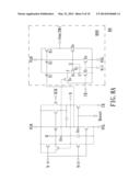
[0010] FIG. 3A is a circuit diagram of a shift register according to an embodiment of the present invention.
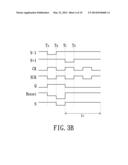
[0011] FIG. 3B is an operating timing diagram of the shift register shown in FIG. 3A.
[0012] FIG. 4 is a circuit diagram of a shift register according to another embodiment of the present invention.
[0013] FIG. 5 is a circuit diagram of a shift register according to another more embodiment of the present invention.
[0014] FIG. 6 is a block diagram of a shift register according to another embodiment of the present invention.
[0015] FIG. 7A is a circuit diagram of a driving-signal generating module according to an embodiment of the present invention.
[0016] FIG. 7B is a circuit diagram of a driving module according to an embodiment of the present invention.
[0017] FIG. 7C is a waveform diagram of signals respectively corresponding to each node when the circuit in FIG. 7B operates.
[0018] FIG. 8A is a circuit diagram of a shift register according to another more again embodiment of the present invention.
[0019] FIG. 8B is a waveform diagram of signals respectively corresponding to each node when the shift register in FIG. 8A operates.
DETAILED DESCRIPTION OF EMBODIMENTS
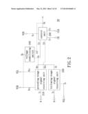
[0020] Referring to FIG. 2, FIG. 2 is a block diagram of a shift register according to an embodiment of the present invention. In this embodiment, supposing that the shift register 20 is the Nth stage of a shift register group, the shift register 20 includes an (N-1)th (previous) signal receiving unit 210, an (N+1)th (next) signal receiving unit 220, a control unit 230, and a voltage stabilizing switch 240.
[0021] The (N-1)th signal receiving unit 210 has an (N-1)th signal input terminal I1, an (N-1)th first preset-voltage input terminal VP1, an (N-1)th second preset-voltage input terminal VP2, an (N-1)th first control-signal output terminal OP1, and an (N-1)th second control-signal output terminal OP2. The (N-1)th signal input terminal I1 receives an (N-1)th signal N-1 outputted from an (N-1)th shift register. The (N-1)th first preset-voltage input terminal VP1 is electrically coupled to a preset voltage source VGH. The (N-1)th second preset-voltage input terminal VP2 is electrically coupled to a preset voltage source VGL. The detailed circuit design of the (N-1)th signal receiving unit 210 will be illustrated as follows by examples and referring to other drawings. However, in summary, the circuit design is needed to make the (N-1)th signal receiving unit 210 capable of controlling degrees of an electrical conduction between the (N-1)th first preset-voltage input terminal VP1 and the (N-1)th first control-signal output terminal OP1 according to a voltage of the (N-1)th signal N-1, and capable of controlling degrees of an electrical conduction between the (N-1)th second preset-voltage input terminal VP2 and the (N-1)th second control-signal output terminal OP2 according to the voltage of the (N-1)th signal N-1.
[0022] The (N+1)th signal receiving unit 220 has an (N+1)th signal input terminal I2, an (N+1)th second preset-voltage input terminal Vf, and an (N+1)th control-signal output terminal Of. The (N+1)th signal input terminal I2 receives an (N+1)th signal N+1 outputted from an (N+1)th shift register. The (N+1)th second preset-voltage input terminal Vf is electrically coupled to the preset voltage source VGL. The (N+1)th control-signal output terminal Of is electrically coupled to the (N-1)th first control-signal output terminal OP1 of the (N-1)th signal receiving unit 210. The detailed circuit design of the (N+1)th signal receiving unit 220 will be illustrated as follows by examples and referring to other drawings. However, in summary, the circuit design is needed to make the (N+1)th signal receiving unit 220 capable of controlling degrees of an electrical conduction between the (N+1)th second preset-voltage input terminal Vf and the (N+1)th control-signal output terminal Of according to a voltage of the (N+1)th signal N+1.
[0023] The control unit 230 has a first preset-voltage input terminal VC, a clock-signal input terminal CC, a reversed clock-signal input terminal CX, a first control-signal input terminal IC1, a second control-signal input terminal IC2, and an output terminal OC. The first preset-voltage input terminal VC is electrically coupled to the preset voltage source VGH. The clock-signal input terminal CC receives a clock signal CK, and the reversed clock-signal input terminal CX receives a reversed clock signal XCK which has a phase reverse to that of the clock signal CK. The first control-signal input terminal IC1 is electrically coupled to the (N-1)th first control-signal output terminal OP1 of the (N-1)th signal receiving unit 210, and the second control-signal input terminal IC2 is electrically coupled to the (N-1)th second control-signal output terminal OP2 of the (N-1)th signal receiving unit 210. The detailed circuit design of the control unit 230 will be illustrated as follows by examples and referring to other drawings. However, in summary, the circuit design is needed to make the control unit 230 capable of controlling degrees of an electrical conduction between the clock-signal input terminal CC and the output terminal OC according to a voltage of the reversed clock signal XCK, a voltage at the first control-signal input terminal IC1 and a voltage at the second control-signal input terminal IC2.
[0024] The voltage stabilizing switch 240 has a control terminal CS, and two source/drain terminals S1 and S2. The control terminal CS is electrically coupled to the output terminal OC of the control unit 230. The source/drain terminal S1 is electrically coupled to the (N-1)th first control-signal output terminal OP1 of the (N-1)th signal receiving unit 210, and the source/drain terminal S2 is electrically coupled to the (N-1)th first preset-voltage input terminal VP1 of the (N-1)th signal receiving unit 210.
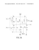
[0025] Referring to FIG. 3A, FIG. 3A is a circuit diagram of a shift register according to an embodiment of the present invention. In this embodiment, the (N-1)th signal receiving unit 210 shown in FIG. 2 includes P type transistors T1 and T4. The (N+1)th signal receiving unit 220 includes a P type transistor T3 and a capacitor C2. The control unit 230 includes P type transistors T5, T6, T7 and T8, and capacitor C1. The voltage stabilizing switch 240 includes P type transistor T2.
[0026] Shown in FIG. 3A, each of the P type transistors T1-T8 has a control terminal, and two source/drain terminals, and each of the capacitors C1 and C2 has two source/drain terminals. In this embodiment, the control terminal of the P type transistor T1 is electrically coupled to the (N-1)th signal input terminal I1, or in other words, the control terminal of the P type transistor T1 is used as the (N-1)th signal input terminal I1. Furthermore, one source/drain terminal of the P type transistor T1 is electrically coupled to the (N-1)th first control-signal output terminal OP1 and a node Q, and the other source/drain terminal of the P type transistor T1 is electrically coupled to the (N-1)th first preset-voltage input terminal VP1 to receive a voltage provided by the preset voltage source VGH. The control terminal of the P type transistor T2 is electrically coupled to the output terminal OC of the control unit 230 shown in FIG. 2. One source/drain terminal of the P type transistor T2 is electrically coupled to the (N-1)th first control-signal output terminal OP1 and the node Q, and the other source/drain terminal of the P type transistor T2 is electrically coupled to the (N-1)th first preset-voltage input terminal VP1 to be electrically coupled to the preset voltage source VGH.
[0027] The control terminal of the P type transistor T3 is electrically coupled to the (N+1)th signal input terminal I2, or in other words, the control terminal of the P type transistor T3 is used as the (N+1)th signal input terminal I2. Furthermore, one source/drain terminal of the P type transistor T3 is electrically coupled to the (N+1)th second preset-voltage input terminal Vf, and the other source/drain terminal of the P type transistor T3 is electrically coupled to the (N+1)th control-signal output terminal Of, and is also electrically coupled to the node Q like as the (N-1)th first control-signal output terminal OP1. The control terminal of the P type transistor T4 is also electrically coupled to the (N-1)th signal input terminal I1 like as the P type transistor T1, one source/drain terminal of the P type transistor T4 is electrically coupled to the (N-1)th second preset-voltage input terminal VP2, and the other source/drain terminal of the P type transistor T4 is electrically coupled to the (N-1)th second control-signal output terminal OP2.
[0028] The control terminal of the P type transistor T5 is electrically coupled to the second control-signal input terminal IC2, and thereby is electrically coupled to the (N-1)th second control-signal output terminal OP2. One source/drain terminal of the P type transistor T5 is electrically coupled to the clock-signal input terminal CC to receive the clock signal CK, and the other source/drain terminal of the P type transistor T5 is electrically coupled to the output terminal OC. The control terminal of the P type transistor T6 is electrically coupled to the first control-signal input terminal IC1, and thereby is electrically coupled to the (N-1)th first control-signal output terminal OP1. One source/drain terminal of the P type transistor T6 is electrically coupled to the second control-signal input terminal IC2, and thereby is electrically coupled to the (N-1)th second control-signal output terminal OP2. The other source/drain terminal of the P type transistor T6 is electrically coupled to the (N-1)th first preset-voltage input terminal VP1 to receive a voltage provided by the preset voltage source VGH.
[0029] The control terminal of the P type transistor T7 is electrically coupled to the first control-signal input terminal IC1, and thereby is also electrically coupled to the (N-1)th first control-signal output terminal OP1 like as the control terminal of the P type transistor T6. One source/drain terminal of the P type transistor T7 is electrically coupled to the output terminal OC, and the other source/drain terminal of the P type transistor T7 is electrically coupled to the first preset-voltage input terminal V. The two source/drain terminals of the P type transistor T8 are electrically coupled to the two source/drain terminals of the P type transistor T7, and the control terminal of the P type transistor T8 is electrically coupled to the reversed clock-signal input terminal CX to receive the reversed clock signal XCK. Finally, one terminal of the capacitor C1 is electrically coupled to the output terminal OC, and the other terminal of the capacitor C1 is electrically coupled to the second control-signal input terminal IC2. One terminal of the capacitor C2 is electrically coupled to the (N+1)th second preset-voltage input terminal Vf, and the other terminal of the capacitor C1 is electrically coupled to the (N+1)th control-signal output terminal Of, and thereby is electrically coupled to the (N-1)th first control-signal output terminal OP1.
[0030] Referring to FIG. 3A and FIG. 3B, FIG. 3B is an operating timing diagram of the shift register shown in FIG. 3A, assuming that logic low level is enable level, the logic high level is non-enable level, the preset voltage source VGH provides a voltage with logic high level, and the preset voltage source VGL provides a voltage with logic low level. So shown as in FIG. 3A and FIG. 3B, before the time point TA, the (N-1)th signal N-1 outputted from the (N-1)th shift register and the (N+1)th signal N+1 outputted from the (N+1)th shift register both are at logic high level (that is, in non-enable state), and the clock signal CK and the reversed clock signal XCK sustain periodic changes with the phase reverse to each other. At this time, the P type transistors T1, T3 and T4 are turned off due to being controlled by the (N-1)th signal N-1 and the (N+1)th signal N+1, and other P type transistors, the node Q, node Boost and an output signal N outputted by the output terminal OC, each keep at a specific level. Briefly, before the time point TA, the level at each node in the shift register 20 keeps in one of three kinds of specific level because of being in an initialized state, an operation result of the shift register 20 in previous time, or level changes due to the turning on/off of the P type transistors T8 by the reversed clock signal XCK.
[0031] Next, between the time point TA and the time point TB, the (N-1)th signal N-1 is turned from the logic high level to the logic low level, therefore the P type transistors T1 and T4 are turned on. The voltage of the node Q is pulled up to be equal or close to the voltage provided by the preset voltage source VGH (that is, the logic high level). In contrast, the voltage of the node Boost is pulled down to be equal or close to the voltage provided by the preset voltage source VGL (that is, the logic low level). At this time, the node Q at the logic high level makes the P type transistors T6 and T7 being turned on. In opposite, the node Boost at the logic low level makes the P type transistor T5 being turned on, and the reversed clock signal XCK at the logic low level makes the P type transistor T8 being turned on. Therefore, the output signal N is pulled up to the logic high level to make the P type transistor T2 being turned off.
[0032] Between the time point TB and the time point TC, the (N-1)th signal N-1 is turned from the logic low level to the logic high level, therefore the P type transistors T1 and T4 are turned off. In addition, the (N+1)th signal N+1 keeps at the logic high level, and the P type transistor T3 keeps in a turned-off state. During this time, the reversed clock signal XCK is turned from the logic low level to the logic high level, the P type transistor T8 is accordingly turned off, and the preset voltage source VGH thereby cannot influence the voltage of the output signal N via the P type transistor T8. However, due to the clock signal CK being turned from the logic high level to the logic low level, except the voltage of the node Boost is further pulled down, the voltage of the output signal N is pulled down to be almost the same logic low level as the clock signal CK due to the P type transistor T5 keeping in a turned-on state. The output signal N being pulling down turns on the P type transistor T2, and makes the voltage of the node Q thereby keeping being equal or close to the voltage provided by the preset voltage source VGH. Furthermore, the P type transistors T6 and T7 thereby keep in the turned-on state to ensure a stabilized operation of the whole circuit.
[0033] Between the time point TC and the time point TD, the (N+1)th signal N+1 is turned from the logic high level to the logic low level, the P type transistor T3 is accordingly turned on, and makes the voltage of the node Q being pulled down to be equal or close to the voltage provided by the preset voltage source VGL. Due to the node Q being pulled down to the logic low level, the P type transistors T6 and T7 are turned on, and further make the voltages of the node Boost and the output signal N being accordingly pulled up to be equal or close to the logic high level. In this state, the P type transistor T5 is turned off due to the node Boost being at the logic high level, and the clock signal CK thereby cannot influence the voltage of the output signal N. In contrast, the reversed clock signal XCK at the logic low level accordingly turns on the P type transistor T8, and the output signal N is also pulled up to be equal or close to the logic high level by being electrically coupled to the preset voltage source VGH via the P type transistor T8. Furthermore, due to the output signal N being turned to the logic high level, the P type transistor T2 is accordingly turned off. Due to the (N-1)th signal N-1 being still at the logic high level, the P type transistor T1 is in the turned-off state. Therefore, the voltage of the node Q keeps at the logic low level and is not pulled up the logic high level provided by the preset voltage source VGH.
[0034] After the time point TD, the (N-1)th signal N-1 and the (N+1)th signal N+1 both keeps at the logic high level, and the P type transistors T1, T3 and T4 are accordingly turned off. Due to the node Q being at the logic low level, the P type transistors T6 and T7 are turned off, and the node Boost and the output signal N are thereby at the logic high level. The output signal N at the logic high level controls the P type transistor T2 to be turned off. When the P type transistors T1 and T2 are turned off, the node Q cannot being electrically coupled to the preset voltage source VGH. Therefore, the voltage of the node Q keeps at the logic low level, and further ensures a stabilized operation of the whole circuit.
[0035] In summary, the voltage of the node Q keeps at a stabilized level in the time interval t1 after the time point TC, therefore, the P type transistor T7 can keep in a stabilized turned-on state, and make the output signal N having a stabilized pulling up voltage source (that is, the preset voltage source VGH). In comparison with the unstable output signal N due to the periodic changes of the voltage at the node Q in the time interval t1 shown in FIG. 1B, the circuit configuration provided by the above embodiment undoubtedly can make the voltage of the output signal N more stabilized.
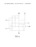
[0036] It should be noted that, although the above embodiment is illustrated by taking the P type transistors as an example, the relative circuit composed all by N type transistors actually can be also employed. Referring to FIG. 4, FIG. 4 is a circuit diagram of a shift register according to another embodiment of the present invention. In this embodiment, the connection between the transistors is the same as that shown in FIG. 3A, so it is not excessively described in detail here. However, the logic low level is a preferred choice to enable the N type transistors, therefore, the portion electrically coupled to the preset voltage source VGH shown in FIG. 3A is changed to be electrically coupled to the preset voltage source VGL shown in FIG. 4, and the portion electrically coupled to the preset voltage source VGL shown in FIG. 3A is changed to be electrically coupled to the preset voltage source VGH shown in FIG. 4. The timing diagram generated in operating of the circuit shown in FIG. 4 is similar to that shown in FIG. 3B, it merely needs to exchange the logic high level and the logic low level of the timing diagram shown in FIG. 3B to obtain the timing diagram proper to the circuit shown in FIG. 4. Furthermore, the operation principle is similar to the embodiment illustrated by FIGS. 3A and 3B, and it is not excessively described in detail here.
[0037] Expect that the target of stabilizing the voltage of the output signal N is achieved by continuously stabilizing the voltage of the node Q, the phenomenon that the voltage is unstable due to the leakage current of the transistors can be further considered. Referring to FIG. 5, FIG. 5 is a circuit diagram of a shift register according to another more embodiment of the present invention. The shift register of this embodiment includes three more P type transistors P3, P4 and P5 than the shift register shown in FIG. 3A to reduce the change generated in the voltage at the node Q caused by the leakage current of the transistors. In this embodiment, the P type transistor P3 is electrically coupled between the P type transistor T1 (corresponding to the P type transistor T1 shown in FIG. 3A) and the preset voltage source VGH, the P type transistor P4 is electrically coupled between the P type transistor T2 (corresponding to the P type transistor T2 shown in FIG. 3A) and the preset voltage source VGH, and the P type transistor P5 is electrically coupled between the P type transistor T2 and the preset voltage source VGL.
[0038] Referring also to FIG. 2, shown as in FIGS. 2 and 5, a control terminal of the P type transistor P3 also receives the (N-1)th signal N-1 like as the control terminal of the P type transistor T1, or the control terminals of the P type transistors P3 and T1 both are electrically coupled to the (N-1)th signal input terminal I1 shown in FIG. 2. One source/drain terminal of the P type transistor P3 is electrically coupled to the node Q, or is also electrically coupled to the (N-1)th first preset-voltage input terminal VP1 of the (N-1)th signal receiving unit 210 shown in FIG. 2, and is thereby electrically coupled to the source/drain terminal of the P type transistor T1. The other source/drain terminal of the P type transistor P3 is electrically coupled to the preset voltage source VGH. Therefore, the P type transistors P3 and T1 are simultaneously turned on/off, and a time of the P type transistor P3 influencing the voltage at the node Q almost equals to a time of the P type transistor T1 influencing the voltage at the node Q.
[0039] Referring also to FIG. 3B, because the P type transistor T1 is turned off after the time point TB shown in FIG. 3B due to the (N-1)th signal N-1 being turned to the logic high level, the P type transistor P3 is also turned off after the time point TB, and the voltage between the P type transistors T1 and P3 keeps at the logic high level. After the voltage of the node Q is pulled down to the logic low level at the time point TC, although the leakage current may be generated at the beginning due to the voltage difference between the two source/drain terminals of each of the P type transistors T1 and T2, the almost same voltage between the two source/drain terminals of the P type transistors P3 can occlude the flow of such leakage current.
[0040] Referring to FIGS. 2 and 5, a control terminal of the P type transistor P4 also receives the output signal N like as the control terminal of the P type transistor T2, or the control terminals of the P type transistors P4 and T2 both are electrically coupled to the output terminal OC of the control unit 230 shown in FIG. 2. One source/drain terminal of the P type transistor P4 is electrically coupled to the (N-1)th first preset-voltage input terminal VP1 shown in FIG. 2, and is thereby electrically coupled to the source/drain terminal of the P type transistor T2. The other source/drain terminal of the P type transistor P4 is electrically coupled to the preset voltage source VGH. Therefore, the P type transistors P4 and T2 are simultaneously turned on/off, and a time of the P type transistor P4 influencing the voltage at the node Q almost equals to a time of the P type transistor T2 influencing the voltage at the node Q.
[0041] Referring also to FIG. 3B, because the P type transistor T2 is turned off after the time point TC shown in FIG. 3B due to the output signal N being turned to the logic high level, the P type transistor P4 is also turned off after the time point TC, and the voltage between the P type transistors T2 and P4 keeps at the logic high level. After the voltage of the node Q is pulled down to the logic low level at the time point TC, although the leakage current may be generated at the beginning due to the voltage difference between the two source/drain terminals of each of the P type transistors T1 and T2, the almost same voltage between the two source/drain terminals of the P type transistors P4 can occlude the flow of such leakage current.
[0042] Referring again to FIGS. 2 and 5, a control terminal of the P type transistor P5 is electrically coupled to the (N-1)th first control-signal output terminal OP1 of the (N-1)th signal receiving unit 210 shown in FIG. 2, and is thereby electrically coupled to the node Q. One source/drain terminal of the P type transistor P5 is electrically coupled to the preset voltage source VGH, and the other source/drain terminal of the P type transistor P5 is electrically coupled to the (N-1)th first preset-voltage input terminal VP1 of the (N-1)th signal receiving unit 210.
[0043] Referring also to FIG. 3B, because the voltage of the node Q is pulled down to the logic low level after the time point TC, the P type transistor P5 is turned on after the time point TC due to the control terminal of the P type transistor P5 is electrically coupled to the node Q. Due to the P type transistor P5 being turned on, the source/drain terminal of the P type transistor T1 connected to the P type transistor P3, and the source/drain terminal of the P type transistor T2 connected to the P type transistor P3 are pulled down to be equal or close to the logic low level provided by the preset voltage source VGL. Therefore, the leakage current caused by the voltage difference between the two source/drain terminals of the P type transistor T1 decreases or even disappears. Similarly, the leakage current caused by the voltage difference between the two source/drain terminals of the P type transistor T2 decreases or even disappears.
[0044] In summary, after the time point TC shown in FIG. 3B, the P type transistors P3 and P4 are added into the circuit to occlude the flow of the leakage current at early period, and the P type transistor P5 is further added to decrease or eliminate the leakage current generated by the P type transistors T1 and T2.
[0045] Similarly, several N type transistors can be added into an circuit configuration composed all by N type transistors to achieve the same target. Such circuit configuration and the operation principle are similar to the above embodiment, and it is not excessively described in detail here.
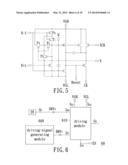
[0046] Referring to FIG. 6, FIG. 6 is a block diagram of a shift register according to another embodiment of the present invention. In this embodiment, the shift register 60 includes the circuit configuration of the shift register 20 shown in FIG. 2, and further includes a driving-signal generating module 600 and a driving module 610. The driving-signal generating module 600 provides a driving signal DRV1, and the phase of the driving signal DRV1 is reverse to the phase of a driving signal DRV2 (that is, the above output signal N) outputted from the output terminal OC of the control unit 230 shown in FIG. 2.
[0047] In this embodiment, the driving module 610 has two input terminals Id1 and Id2, a driving module first preset-voltage input terminal Vd1, a driving module second preset-voltage input terminal Vd2, an enable-signal input terminal IEN, and a driving-signal output terminal Od. The input terminal L is electrically coupled to the driving-signal generating module 600 to receive the driving signal DRV1, and the input terminal Id2 is electrically coupled to the output terminal OC of the control unit 230 to receive the driving signal DRV2. The detailed circuit design of the driving module 610 will be illustrated as follows by examples and referring to other drawings. However, in summary, the circuit design is needed to make the driving module 610 capable of controlling degrees of an electrical conduction between the driving module first preset-voltage input terminal Vd1 and the driving-signal output terminal Od according to the first driving signal DRV1, and capable of controlling degrees of an electrical conduction between the enable-signal input terminal IEN and the driving-signal output terminal Od according to the second driving signal DRV2.
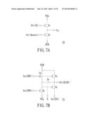
[0048] Referring to FIG. 7A, FIG. 7A is a circuit diagram of a driving-signal generating module according to an embodiment of the present invention. In this embodiment, the driving-signal generating module 70 includes two P type transistors D1 and D2, and each of the P type transistors includes a control terminal and two source/drain terminals. Referring also to FIG. 3A, the control terminal of the P type transistor D1 is electrically coupled to the (N-1)th first control-signal output terminal OP1, and is correspondingly electrically coupled to the node Q. One source/drain terminal of the P type transistor D1 is electrically coupled to the input terminal Idl of the driving module 610, and the other source/drain terminal of the P type transistor D1 is electrically coupled to the preset voltage source VGL. The control terminal of the P type transistor D2 is electrically coupled to the (N-1)th second control-signal output terminal OP2, and is correspondingly electrically coupled to the node Boost. One source/drain terminal of the P type transistor D2 receives the reversed clock signal XCK, and the other source/drain terminal of the P type transistor D2 is electrically coupled to the input terminal Id1 of the driving module 610
[0049] Referring to FIG. 7B, FIG. 7B is a circuit diagram of a driving module according to an embodiment of the present invention. In this embodiment, the driving module 75 includes four P type transistors D3, D4, D5 and D6, and a capacitor DC. Shown as in FIG. 7B, a control terminal of the P type transistor D3 is electrically coupled to the input terminal L to receive the driving signal DRV1. One source/drain terminal of the P type transistor D3 is electrically coupled to the driving-signal output terminal Od, and the other source/drain terminal of the P type transistor D3 is electrically coupled to the preset voltage source VGH. A control terminal of the P type transistor D4 is also electrically coupled to the input terminal Id1 to receive the driving signal DRV1. One source/drain terminal of the P type transistor D4 is electrically coupled to the preset voltage source VGH, and the other source/drain terminal of the P type transistor D4 and one terminal of the capacitor PC are electrically coupled to a node S. The other terminal of the capacitor DC is electrically coupled to the driving-signal output terminal Od. A control terminal of the P type transistor D5 is also electrically coupled to the input terminal Id2 to receive the driving signal DRV2. One source/drain terminal of the P type transistor D5 is electrically coupled to the preset voltage source VGL, and the other source/drain terminal of the P type transistor D5, the other source/drain terminal of the P type transistor D4 and the terminal of the capacitor DC are electrically coupled to the node S. A control terminal of the P type transistor D6 is also electrically coupled to the node S, one source/drain terminal of the P type transistor D6 is electrically coupled to the enable-signal input terminal IEN, and the other source/drain terminal of the P type transistor D6 is electrically coupled to the driving-signal output terminal Od.
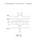
[0050] Referring to FIGS. 7B and 7C, FIG. 7C is a waveform diagram of signals respectively corresponding to each node when the circuit in FIG. 7B operates. Shown as in FIG. 7C, during the time points TG and TH, the driving signal DRV1 is at logic high level, and the driving signal DRV1 is reversely at logic low level. Therefore, the P type transistors D3 and D4 are accordingly turned off, and the P type transistor D5 is accordingly turned on. Thus, the voltage of the node S is firstly influenced by the P type transistor D5 and is pulled down to be about equal to the logic low level provided by the preset voltage source VGL, and is then enabled to be equal to the logic low level according to an enabling signal EN on the enable-signal input terminal IEN being enabled. The voltage of the node S is further pulled down to ensure that the voltage of the enabling signal EN can be properly transmitted to the driving-signal output terminal Od.
[0051] Outside the interval from time point TG to the time point TH, due to the driving signal DRV1 at logic low level, and the driving signal DRV1 at logic high level, the P type transistors D3 and D4 are accordingly turned on, and the P type transistor D5 is accordingly turned off. Therefore, the voltage of the node S is pulled up to be about equal to the logic high level provided by the preset voltage source VGH, and further makes the driving-signal output terminal Od keeping at a level about equal to the logic high level provided by the preset voltage source VGH.
[0052] In summary, only during the time points TG and TH, the voltage at the driving-signal output terminal Od (or driver signal SCAN) can be enabled (in this embodiment, being enabled means being at about logic low level). A duration of the enabling signal EN on the enable-signal input terminal IEN determines a duration t2 when the driver signal SCAN is enabled. That is, the enabled duration of the output signal of the shift register can be properly and dynamically adjusted via the circuit design shown in FIG. 6 or FIGS. 7A and 7B.
[0053] In addition, it should be noted that, shown as in FIG. 7C, just the phases of the driving signals DRV1 and DRV1 are reverse to each other, it does not need to construct a corresponding circuit restrictively according to FIG. 2 or FIG. 6. In other word, it just needs two signals having phases reverse to each other respectively provided to the input terminals L and Id2 as the driving signals DRV1 and DRV1, the target of adjusting the enabled duration of the driver signal SCAN can be achieved via the circuit shown in FIG. 7B utilizing the enabling signal EN in different enabling period. Further, although the circuits shown in FIGS. 7A and 7B is designed mainly with P type transistors, the person having ordinary skill in the art can easily change the design to a circuit mainly composed by N type transistors. Due to such change capable of being achieved under a limited modulation, it is not excessively described here.
[0054] Referring to FIG. 8A, FIG. 8A is a circuit diagram of a shift register according to another more again embodiment of the present invention. In this embodiment, the shift register 80 not only includes all the circuits of the shift register 20, but also further includes an illuminating signal generating unit 800. The illuminating signal generating unit 800 has an illuminating control-signal output terminal OEM to output an illuminating control signal EM. In this embodiment, the illuminating signal generating unit 800 includes eight P type transistors E1˜E8 and a capacitor EC, and each P type transistor includes a control terminal and two source/drain terminals.
[0055] Shown as in FIG. 8A, the control terminals of the P type transistors E1, E2 and E3 are electrically coupled to the (N-1)th second control-signal output terminal OP2 (corresponding to the node Boost), and one source/drain terminal of each of the P type transistors E1, E2 and E3 is electrically coupled to the preset voltage source VGH. The other source/drain terminal of the P type transistor E1 and one source/drain terminal of the P type transistor E4 are electrically coupled to a node J, and the other source/drain terminal of the P type transistor E4 is electrically coupled to the preset voltage source VGL. The control terminal of the P type transistor E4 is electrically coupled to the (N-1)th first control-signal output terminal OP1 (corresponding to the node Q). The other source/drain terminal of the P type transistor E2 and the control terminals of the P type transistors E5 and E6 are electrically coupled to a node U, and the other source/drain terminal of the P type transistor E3 is electrically coupled to the illuminating control-signal output terminal OEM. Further, one source/drain terminal of the P type transistor E5 is electrically coupled to the node J, one source/drain terminal of the P type transistor E6 is electrically coupled to the preset voltage source VGL, and the other source/drain terminal of the P type transistor E6 is electrically coupled to the illuminating control-signal output terminal OEM. The control terminal of the P type transistor E7 receives the clock signal CK, one source/drain terminal of the P type transistor E7 is electrically coupled to the preset voltage source VGL, and the other source/drain terminal of the P type transistor E7, one terminal of the capacitor EC and the other source/drain terminal of the P type transistor E5 are electrically coupled to a node U'. The control terminal of the P type transistor E8 receives the (N+1)th signal N+1, one source/drain terminal of the P type transistor E8 is electrically coupled to the preset voltage source VGL, and the other source/drain terminal of the P type transistor E8 and one source/drain terminal of the P type transistor E2 are electrically coupled to the node U. Two terminals of the capacitor EC are respectively electrically coupled to the node U and the node U'.
[0056] Referring to FIGS. 8A and 8B, FIG. 8B is a waveform diagram of signals respectively corresponding to each node when the shift register in FIG. 8A operates. The waveforms of the (N-1)th signal N-1, the (N+1)th signal N+1, the clock signal CK, the reversed clock signal XCK, the voltage of the node Boost, the voltage of the node Q and the output signal N have been illustrated in the above embodiments, and it is not excessively described here. The operation principle of the illuminating signal generating unit 800 will be focused on as follows.
[0057] Shown as in FIG. 8, at the time point TA, the voltages of the node Q and the clock signal CK are turned from the logic low level to the logic high level, the voltage of the (N+1)th signal N+1 keeps at the logic high level, and the voltage of the node Boost is turned from the logic high level to the logic low level. Correspondingly, the P type transistors E1, E2 and E3 are turned from the turned-off state to the turned-on state, the P type transistors E4 and E7 are turned from the turned-on state to the turned-off state, and the P type transistor E8 keeps at the turned-off state. Therefore, between the time point TA and the time point TB, the voltages of the node J, the node U and the illuminating control-signal output terminal OEM are pulled up to be equal or close to the logic high level of the preset voltage source VGH respectively via the P type transistors E1, E2 and E3, and thereby the P type transistors E5 and E6 are turned off.
[0058] At the time point TB, the voltage of the node Q keeps at the logic high level, the voltage of the clock signal CK is turned from the logic high level to the logic low level, the voltage of the (N+1)th signal N+1 keeps at the logic high level, and the voltage of the node Boost is turned from the logic low level to a lower level. Correspondingly, the P type transistors E1, E2 and E3 keep the turned-on state, the P type transistors E4 and E8 keep the turned-off state, and the P type transistor E7 is turned from the turned-off state to the turned-on state. Therefore, between the time point TB and the time point TC, the voltages of the node J, the node U and the illuminating control-signal output terminal OEM are pulled up to be equal or close to the logic high level of the preset voltage source VGH respectively via the P type transistors E1, E2 and E3, and thereby the voltage of the node U' is pulled down to be equal or close to the logic low level of the preset voltage source VGL via the P type transistor E7.
[0059] At the time point TC, the voltages of the node Q and the (N+1)th signal N+1 are turned from the logic high level to logic low level, the voltage of the clock signal CK is turned from the logic low level to the logic high level, and the voltage of the node Boost is pulled up to the logic high level. Correspondingly, the P type transistors E1, E2, E3 and E7 are turned from the turned-on state to the turned-off state, and the P type transistors E4 and E8 are turned from the turned-off state to the turned-on state. Therefore, between the time point TC and the time point TD, the voltage of the node U is pulled down to be equal or close to the logic low level of the preset voltage source VGL via the P type transistor E8, and further makes the P type transistors E5 and E6 being turned on. Due to the P type transistor E6 being turned on, the voltage of the illuminating control-signal output terminal OEM is pulled down to be equal or close to the logic low level of the preset voltage source VGL via the P type transistor E6.
[0060] By the above circuit design, the illuminating control signal EM with an enabled duration double than that of the clock signal CK can be obtained (in this embodiment, the illuminating control signal EM is enabled within the logic high level). By adjusting or adding or subtracting some electronic components, the enabled duration of the illuminating control signal EM can be designed to be integral multiple of the enabled duration of the clock signal CK. Such alternative design can be obtained by the person having ordinary skill in the art according to the above embodiment, and it is not excessively described here.
[0061] The design according to FIGS. 8A and 8B can provides an accurate multiple relationship between the clock signal CK and the illuminating control signal EM, Therefore, it is particularly suitable for all the displays driven and controlled via analog circuits (e.g., a compensation circuit in AMOLED) to operate.
[0062] In summary, the present invention makes a conducting path of providing voltage to the output terminal being sequentially turned on based on stable means. In comparison with the conventional means of proving the voltage to the output terminal via continuously turning on/off the transistors, the means provided by the present invention doubtlessly makes the output voltage more stable. In addition, the design of freely adjusting the enabling duration of the output terminal can make the application of the shift register of the present invention more flexible.
[0063] While the present invention has been described in terms of what is presently considered to be the most practical and preferred embodiments, it is to be understood that the present invention needs not be limited to the disclosed embodiment. On the contrary, it is intended to cover various modifications and similar arrangements included within the spirit and scope of the appended claims which are to be accorded with the broadest interpretation so as to encompass all such modifications and similar structures.
User Contributions:
Comment about this patent or add new information about this topic:
Images included with this patent application:
 |  |
 |  |
 |  |
 |  |
 |  |
 |
| Similar patent applications: | |
| Date | Title |
|---|---|
| 2014-03-13 | Shift register |
| 2014-04-03 | Shift register |
| 2014-04-17 | Shift register |
| 2014-07-03 | Shift register |
| 2014-07-31 | Bidirectional shift register |
| New patent applications in this class: | |
| Date | Title |
|---|---|
| 2015-12-17 | Shift register unit, gate driving circuit and display panel |
| 2015-11-05 | Shift register circuit |
| 2015-05-14 | Shift register unit, driving method, gate driving circuit and display device |
| 2015-02-12 | Shift register unit, gate driving circuit and display device |
| 2015-02-12 | Shift register unit, driving method thereof, shift register and display device |
| New patent applications from these inventors: | |
| Date | Title |
|---|---|
| 2016-11-17 | Pixel circuit and driving method thereof |
| 2016-04-07 | Pixel driving circuit |
| 2014-12-11 | Display apparatus and driving method thereof |
| 2014-11-13 | Display panel and scanning circuit |
| 2014-02-20 | Active matrix organic light emitting diode circuit and operating method of the same |
| Top Inventors for class "Electrical pulse counters, pulse dividers, or shift registers: circuits and systems" | |
| Rank | Inventor's name |
|---|---|
| 1 | Youichi Tobita |
| 2 | Yung-Chih Chen |
| 3 | Yu-Chung Yang |
| 4 | Kuo-Hua Hsu |
| 5 | Yong Ho Jang |