Patent application title: Method and apparatus involving high-efficiency photovoltaic with p-type oxidant
Inventors:
Yasser R. Shaban (Sofia, BG)
Milen K. Panteleev (Concord, CA, US)
IPC8 Class: AH01L310216FI
USPC Class:
136256
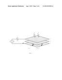
Class name: Photoelectric cells contact, coating, or surface geometry
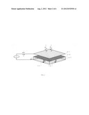
Publication date: 2012-08-02
Patent application number: 20120192938
Abstract:
The present invention is a method and technique (apparatus) to improve
the efficiency of the chemical and physical types of photovoltaics. All
types of photovoltaics suffer from the build-up of counter-electrons,
termed p-type electrons. The p-type electrons induce a potential break to
the main potential of the photovoltaic, i.e. causing a reduction to the
converted power. The application of the oxidant layer to the p-type
semiconductor of the photovoltaic should reduce the p-type electrons from
moving in the external circuit, therefore increases the overall
efficiency.Claims:
1. A method of stopping the emission of p-type electrons in the chemical
and physical structures photovoltaics.
2. An apparatus of stopping the emission of p-type electrons in the chemical and physical structures photovoltaics.
3. Any choice of p-type oxidant: element or substance, for claims 1 and 2.
Description:
CROSS-REFERENCE TO RELATED APPLICATIONS
[0001] Not applicable
STATEMENT REGARDING FEDERALLY SPONSORED RESEARCH OR DEVELOPMENT
[0002] Individual Efforts
BACKGROUND
[0003] Prior and current methods, techniques, and apparatus to generate high efficient solar cells involving:
A) Surface structuring: construction of the cell surface in a pyramid structure, so that incoming light hits the surface several times. For example, U.S. Pat. No. 6,451,218 issued to Holdermann K. on September 2002. B) Tandem or stacked cells: for example, multijunction cell which is based on utilizing a wide spectrum of radiation, different semiconductor materials, which are suited for different spectral ranges, are arranged one on top of the other. For example, U.S. Pat. No. 6,660,928 issued to Patton Martin O et al. on December 2003 and U.S. Pat. No. 6,147,296 issued to Freundlich Alexandre on November 2000. C) Concentrator cells: A higher light intensity will be focused on the solar cells by the use of mirror and lens systems. For example U.S. Pat. No. 7,872,192 issued to Fraas et al. on January 2011 and U.S. Pat. No. 4,069,812 issued to M. J. O'Neill on January 1978.
[0004] The present invention frames the main cause of the inefficiency of the photovoltaics and courses a new method-and-apparatus of improving its efficiency. The inefficiency of the solar cells is caused by the presence of the counter-electrons, termed p-type electrons, which induces a potential break of the photovoltaic i.e. a reduction of the converted power. The photoelectrons are released from the p-type and n-type semiconductor materials depending on the binding energy of the electrons of the applied material and the quantum energy of the incident photon.
[0005] According to electrochemistry, the application of the oxidant layer to the p-type semiconductor of the photovoltaic should reduct the p-type electrons from moving in the external circuit, therefore increases the overall efficiency.
BRIEF DESCRIPTION OF THE DRAWINGS
[0006] Figures included in this invention are briefly described as follows.
[0007] FIG. 1 Illustration of the main components involved in the structure of the chemical photovoltaic. It is also the earlier version of the photovoltaic before the mid of sixtieth.
[0008] FIG. 2 Illustration of the main components involved in the structure of the physical photovoltaic.
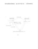
[0009] FIG. 3 The vision of the reduction-diagram; it precisely leads to the selection of the p-type oxidant on the basis of electrochemistry. Only three elements are shown here; hydrogen at the center, fluorine at the right and lithium at the left. The direction of the p-type oxidant is ahead of the p-type semiconductor.
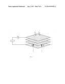
[0010] FIG. 4 The orientation of the electric field, the p-type oxidant, and the direction of the electric current.
[0011] FIG. 5 The course or the importance of the p-type oxidant to the chemical photovoltaic.
[0012] FIG. 6 The course or the importance of the p-type oxidant to the physical photovoltaic.
SUMMARY OF THE INVENTION
[0013] The embodiment of the present invention introduces a unique technique and apparatus for the objective of improving the overall efficiency of the photovoltaics (solar cells). Such method and apparatus (denoted 12 in the diagrams) is implemented by placing a material of higher electrode potential, oxidant, than the electrode potential of the p-type semiconductor (11) or p-type electrode (3) according to the electrochemistry.
[0014] For the physical photovoltaic, the oxidant material (12) is implanted to the structure, or doped to the structure, or mechanically oriented to the structure, in all cases its position is always next to the p-type semiconductor (11). The reason of applying the oxidant material (12) to the solar cell is to stop the generation of the p-type electrons (5) which establishes a counter-flow of electrons (denoted 6 in the diagrams) emitted by the p-type semiconductor (11).
[0015] For the chemical photovoltaic, the oxidant material (12) is placed next to the p-type electrode (3) in order to stop the generation of the p-type electrons (5) which establishes a counter-flow of electrons (6) emitted by the p-type electrode (3).
[0016] The normal direction of the electrons, n-type electrons, is denoted 7 in the diagrams, whereas the normal path of the electric current (8) is always in the opposite direction.
DETAILED DESCRIPTION OF THE INVENTION
[0017] The chemical setup of photovoltaics is illustrated in FIG. 1. As shown in FIG. 1, three main layers characterize the operation of photovoltaic; n-type electrode (1), semiconductor (2), and p-type electrode (3). The emission of the p-type electrons (5) is released as a result of photoelectric effect when light (4) hits the photovoltaic. Such electrons have greater tendency to move (6) in the external circuit when load (9) is present and opposes the direction of the n-type electrons (7) which is the principal photoelectric emitter.
[0018] In the physical setup (FIG. 2), three main layers characterize the operation of photovoltaic; n-type electrode (1), p-n junction semiconductor (10), and p-type semiconductor (11). Similar to the chemical setup, the p-type electrons are released due to photoelectric effect and oppose the direction of the n-type electrons.
[0019] In both types of photovoltaics, the direction of electric current (8) is always in the opposite direction of the n-type electrons (7) and this is the standard and normal behavior.
[0020] When light (4) hits the photovoltaic, a fraction of light is absorbed at the front layer, a fraction is transmitted, a fraction is absorbed in the second layer, and so on. The Einstein's equation of photoelectric effect is given by:
h ν=φ+Ee.
Where h is the Planck's constant, ν is the photon's frequency, φ is the binding energy (the least energy needed for electrons to be liberated from the surface), and Ee is the residual energy of the emitted electrons. For photoelectric effect h ν must be greater than φ. As a result, the emitted electrons would have energy to move in the direction in which the conductivity is the highest--the external circuit.
[0021] The potential and the density of p-type electrons depend on the binding energy of the p-type electrode, the concentration of the p-type atoms, and the fraction of the transmitted photons. These combined factors contribute to the establishment of the counter electrons (6) and reduce the overall efficiency of the photovoltaic since they move in the external circuit and oppose the direction of the n-type electrons. In order to eliminate the negative effect of the p-type electrons we introduce an electron absorber, oxidant, next to the p-type electrode. The introduction of the oxidant material to the photovoltaics can be made chemically (such as solar gel) or physically (such as ion implantation and physical vapor deposition).
[0022] According to electrochemistry, FIG. 3, the choice of the oxidant (12) depends on the choice of the p-type electrode (3) or the p-type semiconductor (11); the types of the dopants and not the semiconductor. (For example, the p-type semiconductor of the silicon wafer photovoltaic is boron).
[0023] The choice of the oxidant (denoted B in the diagram) is fluorine-ward (toward fluorine) and in any case the p-type electrode or p-type semiconductor can be any element or substance behind (denoted A in the diagram). The electrochemical reactions of the combinations A and B are as following:
Photons+A→electron or electrons (oxidation), Here A is ionized positively but there is no charge separation since B is neutralized. B+electron or electrons→(reduction).
[0024] The role of the p-type oxidant not only favors the reduction of the counter electrons (6) but also favors the overall mechanism of the photovoltaic. As shown in FIG. 4, the region of charge separation (10) occurs only in the p-n junction such that the positive charges are drifted toward the n-type (1), whereas the negative charges are drifted toward the p-type (11).
[0025] The migration of electrons in the p-n junction is controlled by the concentration of electrons which must be from the high concentration (n-type) to the low concentration (p-type). On the other hand, the migration of positive carriers is from p-type to n-type. Hence a charge separation takes place. The generation of the electric field E (13) is shown from n-type to p-type which is in the same direction of the electric current, clockwise in the diagram.
[0026] At the p-n junction, an interior electric field (13) is built up which leads to the separation of the charge carriers that are released by light. Through metal contacts, an electric charge can be tapped. If the outer circuit is closed (9), meaning a consumer is connected a direct current flows.
[0027] The role of the p-type oxidant hence accelerate the flow of electric current in the internal circuit by eliminating the generations of the p-type electrons.
[0028] The course of the p-type oxidant (12) in the chemical setup of photovoltaic is shown in FIG. 5.
[0029] The course of the p-type oxidant (12) in the physical setup of photovoltaic is shown in FIG. 6.
[0030] The invention is the p-type oxidant which must be chosen on the basis of electrochemistry and based on the electrode potential of the p-type semiconductor or p-type material in general.
User Contributions:
Comment about this patent or add new information about this topic:
Images included with this patent application:
 |  |
 |  |
 |  |
| Similar patent applications: | |
| Date | Title |
|---|---|
| 2013-08-15 | System and method for determining placement of photovoltaic strips using displacement sensors |
| 2013-08-22 | Conductive film substrate, photovoltaic cell having the same, and method of manufacturing the same |
| 2013-08-22 | Enhancing the photovoltaic response of czts thin-films |
| 2010-12-30 | High efficiency photovoltaic modules |
| 2013-08-08 | Method for manufacturing a photovoltaic cell comprising a tco layer |
| New patent applications in this class: | |
| Date | Title |
|---|---|
| 2022-05-05 | Solar cell element and method for manufacturing solar cell element |
| 2022-05-05 | Photovoltaic module, integrated photovoltaic/photo-thermal module and manufacturing method thereof |
| 2022-05-05 | Method for manufacturing dye-sensitized solar cells and solar cells so produced |
| 2019-05-16 | Solar cell, composite electrode thereon and preparation method thereof |
| 2019-05-16 | Heterojunction solar cell and preparation method thereof |
| New patent applications from these inventors: | |
| Date | Title |
|---|---|
| 2015-07-23 | Coasting-wheel with aeronautic levitation for harmonic electric generation |
| 2013-08-08 | Method and apparatus of deactivating explosives and chemical warfare with high-energy neutrons generated from deuterium tritium fusion reaction |
| 2012-10-25 | Method and apparatus of extracting an immense electric energy from piezoelectric materials in a super-gain energy system |
| Top Inventors for class "Batteries: thermoelectric and photoelectric" | |
| Rank | Inventor's name |
|---|---|
| 1 | Devendra K. Sadana |
| 2 | Mehrdad M. Moslehi |
| 3 | Arthur Cornfeld |
| 4 | Seung-Yeop Myong |
| 5 | Bastiaan Arie Korevaar |