Patent application title: METHOD OF REMOVING PHOTORESIST
Inventors:
Darrell Larue Mcreynolds (Balmain, AU)
Lakshmi C.s. (Balmain, AU)
Yao Fu (Balmain, AU)
Kia Silverbrook (Balmain, AU)
IPC8 Class: AG11B5127FI
USPC Class:
216 27
Class name: Etching a substrate: processes forming or treating thermal ink jet article (e.g., print head, liquid jet recording head, etc.)
Publication date: 2009-03-26
Patent application number: 20090078675
Inventors list |
Agents list |
Assignees list |
List by place |
Classification tree browser |
Top 100 Inventors |
Top 100 Agents |
Top 100 Assignees |
Usenet FAQ Index |
Documents |
Other FAQs |
Patent application title: METHOD OF REMOVING PHOTORESIST
Inventors:
Kia Silverbrook
Lakshmi C.S.
Darrell LaRue McReynolds
Yao Fu
Agents:
SILVERBROOK RESEARCH PTY LTD
Assignees:
Origin: BALMAIN, AU
IPC8 Class: AG11B5127FI
USPC Class:
216 27
Abstract:
A method of photoresist removal is provided. The method employs a plasma
formed from a gas chemistry comprising NH3. The method is
particularly suitable for use in MEMS fabrication processes, such as
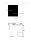
inkjet printhead fabrication.Claims:
1. A method of photoresist removal, said method employing a plasma formed
from a gas chemistry comprising NH.sub.3.
2. The method of claim 1, wherein said gas chemistry consists of NH3 only.
3. The method of claim 1, wherein said gas chemistry further comprises O.sub.2.
4. The method of claim 3, wherein a ratio of O2:NH3 is in the range of 15:1 to 5:1.
5. The method of claim 1, wherein the gas chemistry consists of O2 and NH.sub.3.
6. The method of claim 1, wherein said gas chemistry further comprises N.sub.2.
7. The method of claim 6, wherein a ratio of N2:NH3 is in the range of 5:1 to 1:5.
8. The method of claim 1, wherein the gas chemistry consists of O2, NH3 and N.sub.2.
9. The method of claim 1, wherein a rate of photoresist removal is at least 20% greater than a rate of photoresist removal using an O2 plasma.
10. The method of claim 1, wherein said photoresist is hardbaked photoresist.
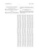
11. The method of claim 1, wherein said photoresist is UV-cured photoresist.
12. The method of claim 1, wherein said photoresist has a thickness of at least 2 microns.
13. The method of claim 1, wherein said photoresist has a thickness of at least 5 microns.
14. The method of claim 1, wherein said method is a step of a MEMS fabrication process.
15. The method of claim 1, wherein said method is a step of a printhead fabrication process.
16. The method of claim 15, wherein said photoresist is contained in at least one of: inkjet nozzle chambers and ink supply channels.
17. The method of claim 15, wherein said photoresist is a protective coating for inkjet nozzle assemblies.
18. A method of fabricating an inkjet printhead, said method comprising the steps of:forming inkjet nozzle chambers on a substrate, each nozzle chamber containing at least some photoresist; andremoving said photoresist using a plasma formed from a gas chemistry comprising NH.sub.3.
Description:
COPENDING APPLICATION
[0001]The following application has been filed by the applicant simultaneously with the present application:
MEMS31US
[0002]The disclosure of this copending application is incorporated herein by reference. The above application has been identified by its filing docket number, which will be substituted with the corresponding application number once assigned.
CROSS REFERENCES TO RELATED APPLICATIONS
[0003]Various methods, systems and apparatus relating to the present invention are disclosed in the following U.S. patents/patent applications filed by the applicant or assignee of the present invention:
TABLE-US-00001 6405055 6628430 7136186 10/920372 7145689 7130075 7081974 7177055 7209257 7161715 7154632 7158258 7148993 7075684 7158809 11/225172 11/474280 11/635482 11/635526 11/650545 11/653241 11/653240 11758648 7241005 7108437 6915140 6999206 7136198 7092130 7249108 6566858 6331946 6246970 6442525 09/517384 09/505951 6374354 7246098 6816968 6757832 6334190 6745331 7249109 10/203559 7197642 7093139 10/636263 10/636283 10/866608 7210038 10/902833 10/940653 10/942858 11/706329 11/757385 11/758642 7170652 6967750 6995876 7099051 11/107942 7193734 11/209711 11/599336 7095533 6914686 7161709 7099033 11/003786 7258417 11/003418 11/003334 11/003600 11/003404 11/003419 11/003700 7255419 11/003618 7229148 7258416 11/003698 11/003420 6984017 11/003699 11/071473 11748482 11/778563 11/779851 11/778574 11/853816 11/853814 11/853786 11/856694 11/003463 11/003701 11/003683 11/003614 11/003702 11/003684 7246875 11/003617 11/764760 11853777 11/293800 11/293802 11/293801 11/293808 11/293809 11/482975 11/482970 11/482968 11/482972 11/482971 11/482969 11/097266 11/097267 11/685084 11/685086 11/685090 11/740925 11/763444 11/763443 11/518238 11/518280 11/518244 11/518243 11/518242 11/084237 11/084240 11/084238 11/357296 11/357298 11/357297 11/246676 11/246677 11/246678 11/246679 11/246680 11/246681 11/246714 11/246713 11/246689 11/246671 11/246670 11/246669 11/246704 11/246710 11/246688 11/246716 11/246715 11/246707 11/246706 11/246705 11/246708 11/246693 11/246692 11/246696 11/246695 11/246694 11/482958 11/482955 11/482962 11/482963 11/482956 11/482954 11/482974 11/482957 11/482987 11/482959 11/482960 11/482961 11/482964 11/482965 11/482976 11/482973 11/495815 11/495816 11/495817 6227652 6213588 6213589 6231163 6247795 6394581 6244691 6257704 6416168 6220694 6257705 6247794 6234610 6247793 6264306 6241342 6247792 6264307 6254220 6234611 6302528 6283582 6239821 6338547 6247796 6557977 6390603 6362843 6293653 6312107 6227653 6234609 6238040 6188415 6227654 6209989 6247791 6336710 6217153 6416167 6243113 6283581 6247790 6260953 6267469 6588882 6742873 6918655 6547371 6938989 6598964 6923526 6273544 6309048 6420196 6443558 6439689 6378989 6848181 6634735 6299289 6299290 6425654 6902255 6623101 6406129 6505916 6457809 6550895 6457812 7152962 6428133 7216956 7080895 11/144844 7182437 11/599341 11/635533 11/607976 11/607975 11/607999 11/607980 11/607979 11/607978 11/735961 11/685074 11/696126 11/696144 11/696650 11/763446 10/407212 7252366 10/683064 10/683041 11766713 11/841647 11/482980 11/563684 11/482967 11/482966 11/482988 11/482989 11/293832 11/293838 11/293825 11/293841 11/293799 11/293796 11/293797 11/293798 11/124158 11/124196 11/124199 11/124162 11/124202 11/124197 11/124154 11/124198 11/124153 11/124151 11/124160 11/124192 11/124175 11/124163 11/124149 11/124152 11/124173 11/124155 7236271 11/124174 11/124194 11/124164 11/124200 11/124195 11/124166 11/124150 11/124172 11/124165 11/124186 11/124185 11/124184 11/124182 11/124201 11/124171 11/124181 11/124161 11/124156 11/124191 11/124159 11/124176 11/124188 11/124170 11/124187 11/124189 11/124190 11/124180 11/124193 11/124183 11/124178 11/124177 11/124148 11/124168 11/124167 11/124179 11/124169 11/187976 11/188011 11/188014 11/482979 11/735490 11/853018 11/228540 11/228500 11/228501 11/228530 11/228490 11/228531 11/228504 11/228533 11/228502 11/228507 11/228482 11/228505 11/228497 11/228487 11/228529 11/228484 11/228489 11/228518 11/228536 11/228496 11/228488 11/228506 11/228516 11/228526 11/228539 11/228538 11/228524 11/228523 11/228519 11/228528 11/228527 11/228525 11/228520 11/228498 11/228511 11/228522 11/228515 11/228537 11/228534 11/228491 11/228499 11/228509 11/228492 11/228493 11/228510 11/228508 11/228512 11/228514 11/228494 11/228495 11/228486 11/228481 11/228477 11/228485 11/228483 11/228521 11/228517 11/228532 11/228513 11/228503 11/228480 11/228535 11/228478 11/228479 6087638 6340222 6041600 6299300 6067797 6286935 6044646 6382769 10/868866 6787051 6938990 11/242916 11/242917 11/144799 11/198235 11/766052 7152972 11/592996 6746105 11/763440 11/763442 11/246687 11/246718 11/246685 11/246686 11/246703 11/246691 11/246711 11/246690 11/246712 11/246717 11/246709 11/246700 11/246701 11/246702 11/246668 11/246697 11/246698 11/246699 11/246675 11/246674 11/246667 11/829957 11/829960 11/829961 11/829962 11/829963 11/829966 11/829967 11/829968 11/829969 7156508 7159972 7083271 7165834 7080894 7201469 7090336 7156489 10/760233 10/760246 7083257 7258422 7255423 7219980 10/760253 10/760255 10/760209 7118192 10/760194 10/760238 7077505 7198354 7077504 10/760189 7198355 10/760232 10/760231 7152959 7213906 7178901 7222938 7108353 7104629 11/446227 11/454904 11/472345 11/474273 7261401 11/474279 11/482939 11/482950 11/499709 11/592984 11/601668 11/603824 11/601756 11/601672 11/650546 11/653253 11/706328 11/706299 11/706965 11/737080 11/737041 11/778062 11/778566 11782593 11/246684 11/246672 11/246673 11/246683 11/246682 7246886 7128400 7108355 6991322 10/728790 7118197 10/728784 10/728783 7077493 6962402 10/728803 7147308 10/728779 7118198 7168790 7172270 7229155 6830318 7195342 7175261 10/773183 7108356 7118202 10/77318 67134744 10/773185 7134743 7182439 7210768 10/773187 7134745 7156484 7118201 7111926 10/773184 7018021 11/060751 11/060805 11/188017 7128402 11/298774 11/329157 11/490041 11/501767 11/499736 7246885 7229156 11/505846 11/505857 11/505856 11/524908 11/524938 7258427 11/524912 11/592999 11/592995 11/603825 11/649773 11/650549 11/653237 11/706378 11/706962 11749118 11/754937 11749120 11/744885 11/779850 11/765439 11842950 11/839539 11/097308 11/097309 7246876 11/097299 11/097310 11/097213 11/210687 11/097212 7147306 7261394 11/764806 11/782595 11/482953 11/482977 11/544778 11/544779 11/764808 09/575197 7079712 6825945 09/575165 6813039 6987506 7038797 6980318 6816274 7102772 09/575186 6681045 6728000 7173722 7088459 09/575181 7068382 7062651 6789194 6789191 6644642 6502614 6622999 6669385 6549935 6987573 6727996 6591884 6439706 6760119 09/575198 6290349 6428155 6785016 6870966 6822639 6737591 7055739 7233320 6830196 6832717 6957768 09/575172 7170499 7106888 7123239 11/066161 11/066160 11/066159 11/066158 11/066165 10/727181 10/727162 10/727163 10/727245 7121639 7165824 7152942 10/727157 7181572 7096137 10/727257 7278034 7188282 10/727159 10/727180 10/727179 10/727192 10/727274 10/727164 10/727161 10/727198 10/727158 10/754536 10/754938 10/727227 10/727160 10/934720 7171323 11/272491 11/474278 11/488853 11/488841 11749750 11749749 10/296522 6795215 7070098 7154638 6805419 6859289 6977751 6398332 6394573 6622923 6747760 6921144 10/884881 7092112 7192106 11/039866 7173739 6986560 7008033 11/148237 7222780 11/248426 11/478599 11/499749 11/738518 11/482981 11/743661 11/743659 11/752900 7195328 7182422 11/650537 11/712540 10/854521 10/854522 10/854488 10/854487 10/854503 10/854504 10/854509 7188928 7093989 10/854497 10/854495 10/854498 10/854511 10/854512 10/854525 10/854526 10/854516 10/854508 7252353 10/854515 7267417 10/854505 10/854493 7275805 10/854489 10/854490 10/854492 10/854491 10/854528 10/854523 10/854527 10/854524 10/854520 10/854514 10/854519 10/854513 10/854499 10/854501 7266661 7243193 10/854518 10/854517 10/934628 7163345 11/499803 11/601757 11/706295 11/735881 11748483 11749123 11/766061 11775135 11772235 11/778569 11/829942 11/014731 11/544764 11/544765 11/544772 11/544773 11/544774 11/544775 11/544776 11/544766 11/544767 11/544771 11/544770 11/544769 11/544777 11/544768 11/544763 11/293804 11/293840 11/293803 11/293833 11/293834 11/293835 11/293836 11/293837 11/293792 11/293794 11/293839 11/293826 11/293829 11/293830 11/293827 11/293828 11/293795 11/293823 11/293824 11/293831 11/293815 11/293819 11/293818 11/293817 11/293816 11/838875 11/482978 11/640356 11/640357 11/640358 11/640359 11/640360 11/640355 11/679786 10/760254 10/760210 10/760202 7201468 10/760198 10/760249 7234802 10/760196 10/760247 7156511 10/760264 7258432 7097291 10/760222 10/760248 7083273 10/760192 10/760203 10/760204 10/760205 10/760206 10/760267 10/760270 7198352 10/760271 10/760275 7201470 7121655 10/760184 7232208 10/760186 10/760261 7083272 11/501771 11/583874 11/650554 11/706322 11/706968 11/749119 11779848 11/855152 11855151 11/014764 11/014763 11/014748 11/014747 11/014761 11/014760 11/014757 11/014714 7249822 11/014762 11/014724 11/014723 11/014756 11/014736 11/014759 11/014758 11/014725 11/014739 11/014738 11/014737 11/014726 11/014745 11/014712 11/014715 11/014751 11/014735 11/014734 11/014719 11/014750 11/014749 7249833 11/758640 11/775143 11/838877 11/014769 11/014729 11/014743 11/014733 11/014754 11/014755 11/014765 11/014766 11/014740 11/014720 11/014753 7255430 11/014744 11/014741 11/014768 11/014767 11/014718 11/014717 11/014716 11/014732 11/014742 11/097268 11/097185 11/097184 11/778567 11852958 11852907 11/293820 11/293813 11/293822 11/293812 11/293821 11/293814 11/293793 11/293842 11/293811 11/293807 11/293806 11/293805 11/293810 11/688863 11/688864 11/688865 11/688866 11/688867 11/688868 11/688869 11/688871 11/688872 11/688873 11/741766 11/482982 11/482983 11/482984 11/495818 11/495819 11/677049 11/677050 11/677051 11/014722 10/760180 7111935 10/760213 10/760219 10/760237 7261482 10/760220 7002664 10/760252 10/760265 7088420 11/446233 11/503083 11/503081 11/516487 11/599312 11/014728 11/014727 7237888 7168654 7201272 6991098 7217051 6944970 10/760215 7108434 10/760257 7210407 7186042 10/760266 6920704 7217049 10/760214 10/760260 7147102 10/760269 7249838 10/760241 10/962413 10/962427 7261477 7225739 10/962402 10/962425 10/962428 7191978 10/962426 10/962409 10/962417 10/962403 7163287 7258415 10/962523 7258424 10/962410 7195412 7207670 11/282768 7220072 11/474267 11/544547 11/585925 11/593000 11/706298 11/706296 11/706327 11/730760 11/730407 11/730787 11/735977 11/736527 11/753566 11/754359 11/778061 11/765398 11/778556 11/829937 11/780470 11/223262 11/223018 11/223114 11/223022 11/223021 11/223020 11/223019 11/014730 7154626 7079292 11/604316
FIELD OF THE INVENTION
[0004]The present invention relates to the field of printers and particularly MEMS inkjet printheads. It has been developed primarily to improve fabrication of MEMS inkjet printheads, although the invention is equally applicable to any MEMS fabrication process.
BACKGROUND OF THE INVENTION
[0005]Many different types of printing have been invented, a large number of which are presently in use. The known forms of print have a variety of methods for marking the print media with a relevant marking media. Commonly used forms of printing include offset printing, laser printing and copying devices, dot matrix type impact printers, thermal paper printers, film recorders, thermal wax printers, dye sublimation printers and ink jet printers both of the drop on demand and continuous flow type. Each type of printer has its own advantages and problems when considering cost, speed, quality, reliability, simplicity of construction and operation etc.
[0006]In recent years, the field of ink jet printing, wherein each individual pixel of ink is derived from one or more ink nozzles has become increasingly popular primarily due to its inexpensive and versatile nature.
[0007]Many different techniques on ink jet printing have been invented. For a survey of the field, reference is made to an article by J Moore, "Non-Impact Printing: Introduction and Historical Perspective", Output Hard Copy Devices, Editors R Dubeck and S Sherr, pages 207-220 (1988).
[0008]Ink Jet printers themselves come in many different types. The utilization of a continuous stream of ink in ink jet printing appears to date back to at least 1929 wherein U.S. Pat. No. 1,941,001 by Hansell discloses a simple form of continuous stream electro-static ink jet printing.
[0009]U.S. Pat. No. 3,596,275 by Sweet also discloses a process of a continuous ink jet printing including the step wherein the ink jet stream is modulated by a high frequency electro-static field so as to cause drop separation. This technique is still utilized by several manufacturers including Elmjet and Scitex (see also U.S. Pat. No. 3,373,437 by Sweet et al)
[0010]Piezoelectric ink jet printers are also one form of commonly utilized ink jet printing device. Piezoelectric systems are disclosed by Kyser et. al. in U.S. Pat. No. 3,946,398 (1970) which utilizes a diaphragm mode of operation, by Zolten in U.S. Pat. No. 3,683,212 (1970) which discloses a squeeze mode of operation of a piezoelectric crystal, Stemme in U.S. Pat. No. 3,747,120 (1972) discloses a bend mode of piezoelectric operation, Howkins in U.S. Pat. No. 4,459,601 discloses a piezoelectric push mode actuation of the ink jet stream and Fischbeck in U.S. Pat. No. 4,584,590 which discloses a shear mode type of piezoelectric transducer element.
[0011]Recently, thermal ink jet printing has become an extremely popular form of ink jet printing. The ink jet printing techniques include those disclosed by Endo et al in GB 2007162 (1979) and Vaught et al in U.S. Pat. No. 4,490,728. Both the aforementioned references disclosed ink jet printing techniques that rely upon the activation of an electrothermal actuator which results in the creation of a bubble in a constricted space, such as a nozzle, which thereby causes the ejection of ink from an aperture connected to the confined space onto a relevant print media. Printing devices utilizing the electro-thermal actuator are manufactured by manufacturers such as Canon and Hewlett Packard.
[0012]As can be seen from the foregoing, many different types of printing technologies are available. Ideally, a printing technology should have a number of desirable attributes. These include inexpensive construction and operation, high speed operation, safe and continuous long term operation etc. Each technology may have its own advantages and disadvantages in the areas of cost, speed, quality, reliability, power usage, simplicity of construction operation, durability and consumables.
[0013]The present Applicant has developed a plethora of inkjet printheads fabricated by MEMS techniques. Typically, MEMS fabrication employs a plurality of photoresist deposition and removal steps. Removal of relatively thin layers of photoresist (c.a. 1 micron or less), used as photolithographic masks, is usually facile. Standard conditions employ an oxygen plasma, which oxidatively removes any photoresist in a process colloquially known in the art as "ashing".
[0014]In the fabrication of inkjet nozzle assemblies, the present Applicant has employed photoresist as a sacrificial scaffold onto which other materials (e.g. heater material, roof structures) may be deposited. This technique enables relatively complex nozzle assemblies to be constructed. However, it requires deposition of relatively thick layers of viscous, heat-resistant photoresist. As will be explained in more detail below, photoresist layers or plugs of up to 30 microns may be required. Furthermore, this photoresist must be thoroughly hardbaked and UV cured so that it does not reflow during subsequent high-temperature deposition steps e.g. deposition of metals or ceramic material onto the photoresist.
[0015]In a typical MEMS printhead fabrication process, a final ashing step removes all remaining photoresist in the nozzle assemblies, including photoresist scaffolds and photoresist plugs employed during the fabrication process. Hitherto, traditional O2 plasma ashing techniques have been employed for final or late-stage removal of photoresist.
[0016]However, thick layers of photoresist, which have been hardbaked and UV cured have increased resistance to ashing and are removed relatively slowly by traditional O2 ashing techniques. This means that prolonged ashing times are required and/or higher ashing temperatures. Prolonged ashing times and/or higher ashing temperatures are undesirable, because there is an increased risk of damage to other MEMS structures (e.g. nozzle chambers, actuators) during the ashing process. Moreover, there is, in general, a need to increase the efficiency of each MEMS processing step so as to reduce processing time and, ultimately, reduce the cost of each printhead.
[0017]The addition of small amounts of fluorine-containing gases (e.g. CF4, C4F8) is known to increase the rate of O2 ashing. However, fluorinated gas chemistries attack materials such as silicon nitride, which typically forms the nozzle plate in the Applicant's MEMS printheads. Accordingly, these ashing conditions are not considered suitable for use in the Applicant's fabrication process.
[0018]The use of O2/N2 has also been used to improve ashing rates, although the addition of N2 shows only moderate improvement over pure O2.
[0019]Accordingly, from the foregoing, it will be appreciated that there is a need to improve the efficiency of photoresist removal in MEMS fabrication techniques. Whilst this need has been presented in the context of printhead fabrication, it will be appreciated that any MEMS fabrication process would benefit from improved techniques for photoresist removal, especially those MEMS fabrication processes which use a relatively thick layer of sacrificial photoresist, which has been hardbaked and/or UV cured.
SUMMARY OF THE INVENTION
[0020]In a first embodiment, there is provided a method of photoresist removal, the method employing a plasma formed from a gas chemistry comprising NH3. The present inventors have found that gas chemistries comprising NH3 are particularly efficacious in removing photoresist and provide higher ashing rates than conventional O2 ashing. Typically ashing rates are improved by at least 20%, at least 50% or at least 100%, compared with ashing rates using a conventional O2 plasma.
[0021]In some embodiments, the gas chemistry consists of NH3 only.
[0022]In other embodiments, the gas chemistry further comprises O2. The O2 may be a major or a minor component of the gas chemistry.
[0023]Optionally a ratio of O2:NH3 is in the range of 15:1 to 5: 1, or optionally about 10:1.
[0024]Optionally, the gas chemistry consists of O2 and NH3.
[0025]Optionally, the gas chemistry further comprises N2.
[0026]Optionally a ratio of N2:NH3 is in the range of 5:1 to 1:5, or optionally about 1:1.
[0027]Optionally, the gas chemistry consists of O2, NH3 and N2, and optionally in a ratio of about 10:1:1.
[0028]Optionally, the photoresist is hardbaked photoresist. Optionally, the photoresist is UV-cured photoresist. Optionally, the photoresist has a thickness of at least 2 microns or at least 5 microns. Traditionally, photoresist of this nature was considered relatively difficult to remove and required prolonged ashing times. However, the present invention removes such photoresist in acceptable times with no damage to other MEMS structures.
[0029]Optionally, the method is a step of a MEMS fabrication process.
[0030]Optionally, the method is a step of a printhead fabrication process.
[0031]Optionally, the photoresist is contained in at least one of: inkjet nozzle chambers and ink supply channels. This photoresist may be used as a sacrificial scaffold during nozzle fabrication, but requires removal in late-stage MEMS processing.
[0032]Optionally, the photoresist is a protective coating for MEMS structures, such as inkjet nozzle assemblies. Typically, MEMS structures are protected with a hardbaked photoresist layer during MEMS fabrication, especially if backside processing steps are required. The present invention is suitable for removing such photoresist.
[0033]In a second aspect, there is provided a method of fabricating an inkjet printhead, the method comprising the steps of:
[0034]forming inkjet nozzle chambers on a substrate, each nozzle chamber containing at least some photoresist; and
[0035]removing said photoresist using a plasma formed from a gas chemistry comprising NH3.
BRIEF DESCRIPTION OF THE DRAWINGS
[0036]Optional embodiments of the present invention will now be described by way of example only with reference to the accompanying drawings, in which:
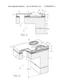
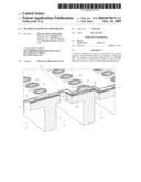
[0037]FIG. 1 is a partial perspective view of an array of nozzle assemblies of a thermal inkjet printhead;
[0038]FIG. 2 is a side view of a nozzle assembly unit cell shown in FIG. 1;
[0039]FIG. 3 is a perspective of the nozzle assembly shown in FIG. 2;
[0040]FIG. 4 shows a partially-formed nozzle assembly after deposition of side walls and roof material onto a sacrificial photoresist layer;
[0041]FIG. 5 is a perspective of the nozzle assembly shown in FIG. 4;
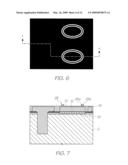
[0042]FIG. 6 is the mask associated with the nozzle rim etch shown in FIG. 7;
[0043]FIG. 7 shows the etch of the roof layer to form the nozzle opening rim;
[0044]FIG. 8 is a perspective of the nozzle assembly shown in FIG. 7;
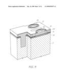
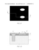
[0045]FIG. 9 is the mask associated with the nozzle opening etch shown in FIG. 10;
[0046]FIG. 10 shows the etch of the roof material to form the elliptical nozzle openings;
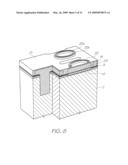
[0047]FIG. 11 is a perspective of the nozzle assembly shown in FIG. 10;
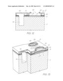
[0048]FIG. 12 shows the nozzle assembly after plasma ashing of the sacrificial photoresist;
[0049]FIG. 13 is a perspective of the nozzle assembly shown in FIG. 12;
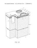
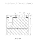
[0050]FIG. 14 shows the whole thickness of the wafer after plasma ashing;
[0051]FIG. 15 is a perspective of the nozzle assembly shown in FIG. 14;
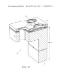
[0052]FIG. 16 is the mask associated with the backside etch shown in FIG. 17;
[0053]FIG. 17 shows the backside etch of the ink supply channel into the wafer; and
[0054]FIG. 18 is a perspective of the nozzle assembly shown in FIG. 17.
DESCRIPTION OF OPTIONAL EMBODIMENTS
[0055]As foreshadowed above, the present invention may be used in connection with any process requiring removal of photoresist. However, it will now be exemplified using the example of MEMS inkjet printhead fabrication. The present Applicant has previously described a fabrication of a plethora of inkjet printheads for which the present invention is suitable. It is not necessary to describe all such printheads here for an understanding of the present invention. However, the present invention will now be described in connection with a thermal bubble-forming inkjet printhead and a mechanical thermal bend actuated inkjet printhead. Advantages of the present invention will be readily apparent from the discussion that follows.
[0056]Referring to FIG. 1, there is shown a part of printhead comprising a plurality of nozzle assemblies. FIGS. 2 and 3 show one of these nozzle assemblies in side-section and cutaway perspective views.
[0057]Each nozzle assembly comprises a nozzle chamber 24 formed by MEMS fabrication techniques on a silicon wafer substrate 2. The nozzle chamber 24 is defined by a roof 21 and sidewalls 22 which extend from the roof 21 to the silicon substrate 2. As shown in FIG. 1, each roof is defined by part of a nozzle plate 56, which spans across an ejection face of the printhead. The nozzle plate 56 and sidewalls 22 are formed of the same material, which is deposited by PECVD over a sacrificial scaffold of photoresist during MEMS fabrication. Typically, the nozzle plate 56 and sidewalls 21 are formed of a ceramic material, such as silicon dioxide or silicon nitride. These hard materials have excellent properties for printhead robustness, and their inherently hydrophilic nature is advantageous for supplying ink to the nozzle chambers 24 by capillary action.
[0058]Returning to the details of the nozzle chamber 24, it will be seen that a nozzle opening 26 is defined in a roof of each nozzle chamber 24. Each nozzle opening 26 is generally elliptical and has an associated nozzle rim 25. The nozzle rim 25 assists with drop directionality during printing as well as reducing, at least to some extent, ink flooding from the nozzle opening 26. The actuator for ejecting ink from the nozzle chamber 24 is a heater element 29 positioned beneath the nozzle opening 26 and suspended across a pit 8. Current is supplied to the heater element 29 via electrodes 9 connected to drive circuitry in underlying CMOS layers of the substrate 2. When a current is passed through the heater element 29, it rapidly superheats surrounding ink to form a gas bubble, which forces ink through the nozzle opening. By suspending the heater element 29, it is completely immersed in ink when the nozzle chamber 24 is primed. This improves printhead efficiency, because less heat dissipates into the underlying substrate 2 and more input energy is used to generate a bubble.
[0059]As seen most clearly in FIG. 1, the nozzles are arranged in rows and an ink supply channel 27 extending longitudinally along the row supplies ink to each nozzle in the row. The ink supply channel 27 delivers ink to an ink inlet passage 15 for each nozzle, which supplies ink from the side of the nozzle opening 26 via an ink conduit 23 in the nozzle chamber 24.
[0060]The complete MEMS fabrication process for manufacturing such printheads was described in detail in our previously filed U.S. application Ser. No. 11/246,684 filed on Oct. 11, 2005, the contents of which is herein incorporated by reference. The latter stages of this fabrication process are briefly revisited here so as to illustrate one example of the present invention.
[0061]FIGS. 4 and 5 show a partially-fabricated printhead comprising a nozzle chamber 24 encapsulating sacrificial photoresist 16. During nozzle fabrication, the photoresist 16 was used firstly to plug the ink inlet 15 (shown in FIG. 2), secondly as a scaffold for deposition of heater material to form the suspended heater element 29, and thirdly as a scaffold for deposition of the sidewalls 22 and roof 21 (which defines part of the nozzle plate 56). The photoresist plugging the ink inlet 15 has a depth of about 20 microns, while the photoresist used as a scaffold in the nozzle chambers has a thickness of at least 5 microns. Furthermore, all the photoresist 16 was hardbaked and UV cured and must be removed later on in the fabrication process.
[0062]Referring to FIGS. 6 to 8, the next stage of MEMS fabrication defines the elliptical nozzle rim 25 in the roof 21 by etching away 2 microns of roof material 20. This etch is defined using a layer of photoresist (not shown) exposed by the dark tone rim mask shown in FIG. 6. The elliptical rim 25 comprises two coaxial rim lips 25a and 25b, positioned over their respective thermal actuator 29.
[0063]Referring to FIGS. 9 to 11, the next stage defines an elliptical nozzle aperture 26 in the roof 21 by etching all the way through the remaining roof material 20, which is bounded by the rim 25. This etch is defined using a layer of photoresist (not shown) exposed by the dark tone roof mask shown in FIG. 9. The elliptical nozzle aperture 26 is positioned over the thermal actuator 29, as shown in FIG. 11.
[0064]With all the MEMS nozzle features now fully formed, the next stage removes the photoresist 16 by frontside plasma ashing (FIGS. 12 and 13). FIGS. 14 and 15 show the entire thickness (150 microns) of the silicon wafer 2 after ashing away all the photoresist 16.
[0065]In a traditional ashing processes, an O2 plasma is employed for ashing the photoresist 16. However, in accordance with the present invention, the ashing plasma is formed using a gas chemistry comprising NH3. When the plasma is formed from a gas chemistry comprising NH3, superior ashing is achieved in terms of increased ashing rate and reduced damage to nozzle structures. Experimental details of ashing conditions are described in more detail in the Example section below.
[0066]Referring to FIGS. 16 to 18, once frontside MEMS processing of the wafer is completed, ink supply channels 27 are etched from the backside of the wafer to meet with the ink inlets 15 using a standard anisotropic DRIE. This backside etch is defined using a layer of photoresist (not shown) exposed by the dark tone mask shown in FIG. 16. The ink supply channel 27 makes a fluidic connection between the backside of the wafer and the ink inlets 15.
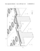
[0067]Finally, and referring to FIGS. 2 and 3, the wafer is thinned to about 135 microns by backside etching. FIG. 1 shows three adjacent rows of nozzles in a cutaway perspective view of a completed printhead integrated circuit. Each row of nozzles has a respective ink supply channel 27 extending along its length and supplying ink to a plurality of ink inlets 15 in each row. The ink inlets, in turn, supply ink to the ink conduit 23 for each row, with each nozzle chamber receiving ink from a common ink conduit for that row.
[0068]It will be appreciated by the person skilled in the art that the exact ordering of late-stage MEMS fabrication steps may be varied. For example, backside ashing may be performed after the ink supply channels 27 have been etched. Alternatively, both frontside and backside ashing may be employed so as to completely remove the photoresist, whilst minimizing risk of damage to nozzle stuctures. Regardless, it will be appreciated that the wafer must be subjected to ashing, either frontside ashing and/or backside ashing, in order to remove the photoresist 16 and furnish the printhead.
EXAMPLES
[0069]Frontside ashing of the nozzle assembly shown in FIGS. 10 and 11 was performed in an ashing oven, using Recipes 1 to 3 shown in Table 1. The temperature in Table 1 refers to the chuck temperature, which is cooled using helium.
TABLE-US-00002 TABLE 1 Recipe 1 Recipe 2 Recipe 3 Pressure (mTorr) 50 50 50 ICP Power (W) 2200 1500 2200 NH3 (sccm) 100 10 10 O2 (sccm) 0 100 100 N2 (sccm) 0 0 10 Temperature (° C.) -5 -5 -5
[0070]Under all the conditions shown in Table 1, an excellent rate of photoresist removal was observed with no observable damage to either the nozzle roof 21 or the heater element 29. In particular, all the photoresist contained in the nozzle chamber was removed after about 15-30 minutes using the conditions shown in Recipes 2 and 3. By way of comparison, conventional O2 ashing or O2/N2 ashing requires about 70-90 minutes of frontside ashing time to remove the same photoresist.
[0071]As expected, the improved ashing rates were also observed in similar backside ashing experiments. Again, the O2/NH3 and the O2/NH3/N2 gas chemistries gave the highest ashing rates, although NH3 only was still superior to O2 only or O2/N2 gas chemistries.
[0072]From these experiments, it can be concluded that gas chemistries comprising NH3 provide superior ashing rates compared to conventional ashing conditions. Moreover, the structural integrity of the MEMS nozzle assemblies is not compromised using these improved ashing conditions.
[0073]The best results were obtained using O2/NH3 and O2/N2/NH3 gas chemistries. However, NH3 only is still superior to conventional O2 ashing conditions.
[0074]It will be appreciated by ordinary workers in this field that numerous variations and/or modifications may be made to the present invention as shown in the specific embodiments without departing from the spirit or scope of the invention as broadly described. The present embodiments are, therefore, to be considered in all respects to be illustrative and not restrictive.
User Contributions:
comments("1"); ?> comment_form("1"); ?>Inventors list |
Agents list |
Assignees list |
List by place |
Classification tree browser |
Top 100 Inventors |
Top 100 Agents |
Top 100 Assignees |
Usenet FAQ Index |
Documents |
Other FAQs |
User Contributions:
Comment about this patent or add new information about this topic:
Images included with this patent application:
 |  |
 |  |
 |  |
 |  |
 |  |
 |  |
 |  |
 |
| Similar patent applications: | |
| Date | Title |
|---|---|
| 2011-07-21 | Method of descumming patterned photoresist |
| 2011-06-16 | Method of removing post-etch residues |
| 2010-02-04 | Method of forming capacitors |
| 2011-01-06 | Methods of forming capacitors |
| 2013-03-21 | Method of producing porous glass |
| New patent applications in this class: | |
| Date | Title |
|---|---|
| 2017-08-17 | Method for manufacturing liquid ejection head |
| 2016-06-02 | Ink-jet recording head, recording element substrate, method for manufacturing ink-jet recording head, and method for manufacturing recording element substrate |
| 2015-12-03 | Method of manufacturing an inkjet head |
| 2015-10-15 | Method for manufacturing liquid ejection head |
| 2015-05-14 | Method for manufacturing liquid discharge head |
| New patent applications from these inventors: | |
| Date | Title |
|---|---|
| 2017-06-15 | Inkjet printhead assembly having ink and air passages |
| 2017-05-18 | Inkjet printhead assembly having printhead chip carriers received in slot |
| 2016-06-09 | Inkjet printer having ink distribution stack for receiving ink from ink ducting structure |
| 2015-11-26 | Inkjet printhead assembly including slotted shield plate |
| 2015-07-16 | Method of wiping pagewidth printhead |
| Top Inventors for class "Etching a substrate: processes" | |
| Rank | Inventor's name |
|---|---|
| 1 | Yoshiyuki Kamata |
| 2 | Masatoshi Sakurai |
| 3 | Shou-Shan Fan |
| 4 | Yi Zheng |
| 5 | Hironori Araki |