Patent application title: Method of manufacturing multilayer printed circuit board
Inventors:
Yoshihiko Shiraishi (Nagoya-City, JP)
Kouji Kondo (Toyohashi-City, JP)
Yoshitaro Yazaki (Anjo-City, JP)
Atusi Sakaida (Nagoya-City, JP)
Assignees:
DENSO CORPORATION
IPC8 Class: AC23F100FI
USPC Class:
216 18
Class name: Forming or treating electrical conductor article (e.g., circuit, etc.) forming or treating of groove or through hole filling or coating of groove or through hole with a conductor to form an electrical interconnection
Publication date: 2009-03-05
Patent application number: 20090057265
ing a multilayer printed circuit board, a
plurality of insulating substrates each having a first surface and a
second surface is prepared. A circuit pattern is formed on each of the
first surfaces of the insulating substrates. A plurality of via holes is
provided so as to extend through respective ones of the insulating
substrates from a side of the second surfaces in such a manner that the
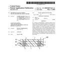
via holes reach corresponding ones of the circuit patterns. Ones of a
plurality of sintered bodies made of conductive particles is inserted
into corresponding ones of the via holes and is fixed in the via holes.
The insulating substrates are stacked so that the circuit patterns are
electrically coupled through the sintered bodies.Claims:
1. A method of manufacturing a multilayer printed circuit board,
comprising:preparing a plurality of insulating substrates each having a
first surface and a second surface;forming a circuit pattern on each of
the first surfaces of the plurality of insulating substrates to form a
plurality of the circuit patterns;providing a plurality of via holes that
extend through respective ones of the plurality of insulating substrates
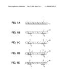
from a side of the second surfaces such that the plurality of via holes
reaches corresponding ones of the plurality of the circuit
patterns;inserting ones of a plurality of sintered bodies into
corresponding ones of the plurality of via holes, the plurality of
sintered bodies formed by sintering a plurality of aggregation of
conductive particles;fixing the plurality of sintered bodies into the
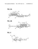
plurality of via holes; andstacking the plurality of insulating
substrates and electrically coupling the plurality of circuit patterns
through the plurality of sintered bodies.
2. The method according to claim 1, whereinthe conductive particles include silver particles and tin particles.
3. The method according to claim 2, whereina tin content of the whole conductive particles is in a range from about 20% to about 80% by weight.
4. The method according to claim 3, whereinthe tin content of the whole conductive particles is in a range from about 30% to about 50% by weight.
5. The method according to claim 1, whereina ratio of a maximum dimension of each of the plurality of sintered bodies to a thickness of each of the plurality of insulating substrates is in a range from about 1 to about 1.4.
6. The method according to claim 5, whereinthe ratio of the maximum dimension of the each of the plurality of sintered bodies to the thickness of the each of the plurality of insulating substrates is in a range from about 1 to about 1.3.
7. The method according to claim 1, whereineach of the plurality of sintered bodies is deformed when the plurality of sintered bodies is fixed into the plurality of via holes.
8. The method according to claim 7, wherein:the ones of the plurality of sintered bodies and the corresponding ones of the plurality of via holes have a clearance therebetween when the ones of the plurality of sintered bodies is inserted into the corresponding ones of the plurality of via holes; andthe deformation amount of the plurality of sintered bodies is let into the clearance when the plurality of sintered bodies is fixed into the plurality of via holes.
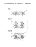
9. The method according to claim 1, wherein a manufacturing method of the plurality of sintered bodies includes:mixing the conductive particles that includes silver particles and tin particles with a solvent to provide a paste;forming the paste into a predetermined shape by using a mask;sintering the paste; andrinsing the sintered paste for removing a carbide.
10. A method of manufacturing a multilayer printed circuit board, comprising:preparing a plurality of insulating substrates each having a first surface and a second surface;forming a circuit pattern on each of the first surfaces of the plurality of insulating substrates to form the plurality of circuit patterns;providing a plurality of via holes that extend through respective ones of the plurality of insulating substrates from a side of the second surfaces such that the plurality of via holes reaches corresponding ones of the plurality of the circuit patterns;inserting ones of a plurality of sintered bodies into corresponding ones of the plurality of via holes, the plurality of sintered bodies formed by sintering a plurality of aggregation of conductive particles, the plurality of sintered bodies having a height that is less than a depth of the plurality of via holes;stacking the plurality of insulating substrates in such a manner that ones of the plurality of the circuit patterns is fitted into corresponding ones of the plurality of via holes; andpressing the stacked insulating substrates during heating so that the ones of the plurality of the circuit patterns comes in contact with corresponding ones of the plurality of the sintered bodies in the corresponding via holes and the plurality of circuit patterns is electrically coupled through the plurality of sintered bodies.
11. The method according to claim 10, whereinthe conductive particles include silver particles and tin particles.
12. The method according to claim 11, whereina tin content of the whole conductive particles is in a range from about 20% to about 80% by weight.
13. The method according to claim 12, whereinthe tin content of the whole conductive particles is in a range from about 30% to about 50% by weight.
14. The method according to claim 10, wherein:an exposed surface of the ones of the plurality of sintered bodies is positioned at a predetermined distance from an open end of the corresponding ones of the plurality of via holes when the ones of the plurality of sintered bodies is inserted into the corresponding ones of the plurality of via holes; andthe predetermined distance is less than or equal to a thickness of the plurality of the circuit patterns.
15. The method according to claim 10, wherein a manufacturing method of the plurality of sintered bodies includes:mixing the conductive particles that includes silver particles and tin particles with a solvent to provide a paste;forming the paste into a predetermined shape by using a mask;sintering the paste; andrinsing the sintered paste for removing a carbide.Description:
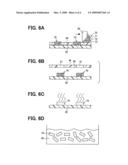
CROSS REFERENCE TO RELATED APPLICATIONS
[0001]The present application is based on and claims priority to Japanese Patent Application No. 2007-224596 filed on Aug. 30, 2007, the contents of which are incorporated in their entirety herein by reference.
BACKGROUND OF THE INVENTION
[0002]1. Field of the Invention
[0003]The present invention relates to a method of manufacturing a multilayer printed circuit board.
[0004]2. Description of the Related Art
[0005]In a conventional manufacturing method of a multilayer printed circuit board, via holes provided in a plurality of resin films are filled with a conductive paste. The conductive paste includes metal particles, an organic solvent, and resin that functions as a binder. Each of the resin films has a circuit pattern layer. The resin films are stacked and the multilayered circuit patterns are electrically coupled through the conductive paste as described, for example, in U.S. Pat. No. 6,889,433 corresponding to JP-A-2001-24323.
[0006]In the present manufacturing method, when the conductive paste is filled into the via holes, a protective film is attached to a surface of the resin film. Thereby, the conductive paste is prevented from attaching to the surface of the resin film except for the via holes. The protective film is removed from the resin film after drying the organic solvent in the conductive paste.
[0007]However, when the protective film is removed, the conductive paste may collapse or may fall on the resin film. Thereby, a conducting abnormality or a short circuit abnormality may occur. Particularly, when a conductive paste having a high metal content rate is used for improving a conductivity of connecting portions, the above-descried disadvantage becomes more serious.
SUMMARY OF THE INVENTION
[0008]In view of the foregoing problems, it is an object of the present invention to provide a manufacturing method of a multilayer printed circuit board that can prevent a conducting abnormality due to an insufficient conductive paste or a short circuit abnormality due to a fallen conductive paste.
[0009]In accordance with a first aspect of a method of manufacturing a multilayer printed circuit board, a plurality of insulating substrates each having a first surface and a second surface is prepared. A circuit pattern is formed on each of the first surfaces of the plurality of insulating substrates to form the plurality of the circuit patterns. A plurality of via holes is provided so as to extend through respective ones of the plurality of insulating substrates from a side of the second surfaces in such a manner that the plurality of via holes reaches corresponding ones of the plurality of the circuit patterns. Ones of a plurality of sintered bodies is inserted into corresponding ones of the plurality of via holes, in which the plurality of sintered bodies is formed by sintering a plurality of aggregation of conductive particles. The plurality of sintered bodies is fixed into the plurality of via holes. The plurality of insulating substrates is stacked and the plurality of circuit patterns is electrically coupled through the plurality of sintered bodies.
[0010]In the present manufacturing method, the circuit patterns can be electrically coupled without filling a conductive paste into the via holes. Thus, a protective film that is used for filling the conductive paste is not required, and thereby the manufacturing process can be simplified. Furthermore, a fall of the conductive paste or a spill of the conductive paste, which can possibly occur when the protective film is removed, can be prevented.
[0011]In accordance with a second aspect of a method of manufacturing a multilayer printed circuit board, a plurality of insulating substrates each having a first surface and a second surface is prepared. A circuit pattern is formed on each of the first surfaces of the plurality of insulating substrates to form the plurality of the circuit patterns. A plurality of via holes is provided so as to extend through respective ones of the plurality of insulating substrates from a side of the second surfaces in such a manner that the plurality of via holes reaches corresponding ones of the plurality of the circuit patterns. Ones of a plurality of sintered bodies is inserted into corresponding ones of the plurality of via holes, in which the plurality of sintered bodies is formed by sintering a plurality of aggregation of conductive particles and the plurality of sintered bodies has a height that is less than a depth of the plurality of via holes. The plurality of insulating substrates is stacked in such a manner that ones of the plurality of circuit patterns is fitted into corresponding ones of the plurality of via holes. The stacked insulating substrates are pressed during heating so that the ones of the plurality of the circuit patterns comes in contact with corresponding ones of the plurality of sintered bodies in the corresponding ones of the plurality of via holes and the plurality of circuit patterns is electrically coupled through the plurality of sintered bodies.
[0012]In the present manufacturing method, effects similar to the manufacturing method according to the first aspect can be obtained. In addition, because a process for fixing the sintered bodies into the via holes is performed at the same time where the multilayered circuit patterns are electrically coupled, the manufacturing process can be further simplified.
BRIEF DESCRIPTION OF THE DRAWINGS
[0013]Additional objects and advantages of the present invention will be more readily apparent from the following detailed description of preferred embodiments when taken together with the accompanying drawings. In the drawings:
[0014]FIG. 1A-FIG. 1E are cross-sectional diagrams illustrating an exemplary manufacturing process of a multilayer printed circuit board according to a first embodiment;
[0015]FIG. 2A and FIG. 2B are diagrams illustrating an exemplary sintered-body inserting process;
[0016]FIG. 3 is a diagram illustrating an exemplary sintered-body fixing process;
[0017]FIG. 4 is a diagram illustrating an exemplary circuit-pattern coupling process;
[0018]FIG. 5A and FIG. 5B are diagrams illustrating an exemplary circuit-pattern coupling process according to a second embodiment; and
[0019]FIG. 6A to FIG. 6D are diagrams illustrating an exemplary manufacturing process of sintered bodies according to a third embodiment.
DETAILED DESCRIPTION OF THE PREFERRED EMBODIMENTS
First Embodiment
[0020]A method of manufacturing a multilayer printed circuit board according to a first embodiment will be described with reference to FIG. 1A to FIG. 4.
[0021]At first, as illustrated in FIG. 1A, a conductive metal layer 2 is attached on a first surface of an insulation resin film 1 that functions as an insulating substrate. The resin film 1 is a thermoplastic resin film having a thickness between about 25 μm and about 75 μm. For example, the resin film 1 consists of between about 65% and about 35% polyether ether ketone resin and between about 35% and about 65% polyetherimide resin by weight. The metal layer 2 is made of copper and has a thickness about 18 μm, for example.
[0022]Then, a circuit-pattern forming process for forming a circuit pattern 3 on the first surface of the resin film 1 is performed. For example, the circuit-pattern forming process can be performed by etching, printing, deposition, or plating. In the present embodiment, the circuit pattern 3 is formed by an etching process. In the etching process, the metal layer 2 is etched from the first surface side of the resin film 1 as illustrated in FIG. 1B. Thereby, a first circuit pattern film 10 is formed.
[0023]Next, as illustrated in FIG. 1C, a via-hole providing process is performed by irradiating a carbon gas laser from a second surface side of the resin film 1. Thereby, a plurality of via holes 4 is provided so as to extend through the resin film 1 and the circuit pattern 3 becomes the bottom of the via holes 4. Accordingly, a second pattern film 20 is formed. An opening diameter of the via holes 4 is determined in such a manner that one of sintered bodies 5 can be inserted into corresponding ones of the via holes 4 in a sintered-body inserting process. Thus, the opening diameter is larger than the maximum dimension of the sintered bodies 5. The sintered bodies 5 may have a sphere shape, a column shape, a rectangular solid shape, or cube shape, for example.
[0024]Portions of the circuit pattern 3 that are located at the bottom of the via holes 4 function as electrodes when multilayered circuit patterns 3 are electrically coupled in a circuit-pattern coupling process. When the via holes 4 are provided, an output power and an irradiation time of the carbon gas laser is controlled so that a hole does not extend in the circuit pattern 3.
[0025]As a substitute for the carbon gas laser, an excimer laser can be used for providing the via holes 4, for example. The via-hole providing process may be also performed by using a drill. By using a laser beam, the via holes 4 can be made small and excessive damage to the circuit pattern 3 can be prevented.
[0026]Next, in a sintered-body inserting process, ones of the sintered bodies 5 is inserted into corresponding ones of the via holes 4, as illustrated in FIG. 1D. Accordingly, a third circuit pattern film 30 is formed. The sintered bodies 5 are formed by sintering aggregations of conducting particles. The sintered bodies 5 may have a height same as open ends of the via holes 4, for example. Alternatively, the sintered bodies 5 may slightly protrude from the open ends of the via holes 4. Each of the via holes 4 is provide to have a clearance between an inner surface of the via hole 4 and an outer surface of sintered body 5. In the present case, when the sintered bodies 5 are deformed in a sintered-body fixing process, the deformation amount can be let into the clearance.
[0027]In order to form the sintered bodies 5, the aggregations are formed from several kinds of conducting particles under a pressurized condition so as to have a predetermined shape and a predetermined size. Then, the aggregations are heated at a temperature under a melting point. Thereby, the conductive particles have a bonding force therebetween and the aggregations are solidified. The sintered bodies 5 inserted in the via holes 4 become coupling members 6 in the circuit-pattern coupling process.
[0028]In the present embodiment, the conducting particles include silver (Ag) particles and tin (Sn) particles. A tin content of the whole conducing particles is in a range from about 20% to about 80% by weight. During experimentation, superior results are observed when the tin content is in a range from about 30% to about 50% by weight. When the tin content is less than about 20% by weight or when the tin content is greater than about 80% by weight, alloy layers provided between bonded interfaces of the aggregations become thin. Thus, a valance between a conductive property and a bonding property may become worse compared with a case where the tin content is in a range from about 20% to about 80%. When the tin content is in a range from about 30% to about 50% by weight, the valance between the conductive property and the bonding property is improved.
[0029]In a process for forming the sintered bodies 5 to have a sphere shape, a mixture of the tin particles and the silver particles are heated at a high temperature. The heated mixture is sprayed on a rotating disk and is dispersed by centrifugal force so as to have a predetermined particle size. Then, the spheres of the mixture are cooled to a predetermined temperature. Thereby, the sphere-shaped sintered bodies 5 including Ag3Sn and Ag.Sn solid solution are formed.
[0030]When the thickness of the resin film 1 is expressed by thickness T, the maximum dimension of each sintered body 5 is in a range from T to 1.4 T. During experimentation, superior results are observed when the maximum dimension of each sintered body 5 is in a range from T to 1.3 T. In a case where each sintered body 5 has a sphere shape, the maximum dimension is a diameter. When each sintered body 5 has the maximum dimension in a range from T to 1.4 T, the conductive property and the bonding property are appropriate as a sintered body made of tin particles and silver particles. For example, when the resin film 1 has a thickness of 75 μm and the circuit pattern 3 made of a copper film has a thickness of 18 μm, the sintered bodies 5 are formed to have a diameter of 90 μm. In the present case, even if the sintered bodies 5 have production variations, the diameters of the sintered bodies 5 are within a range from T to 1.4 T.
[0031]The sintered-body inserting process will now be described with reference to FIGS. 2A and 2B. The sintered-body inserting process is performed by using an inserting apparatus, for example.
[0032]The inserting apparatus includes a metal mask 63, and a rotational moving body 60. The metal mask 63 has a plurality of through holes 64. The rotational moving body 60 includes a rotating part 61 and a curtain part 62 that hangs from the rotating part 61. The inserting apparatus introduces the sintered bodies 5 into the via holes 4 one by one. A diameter of the through holes 64 is set in such a manner that ones of the sintered bodies 5 can fall through corresponding ones of the through holes 64. The through holes 64 extend through the metal mask 63 so as to correspond to the via holes 4 extend through the second pattern film 20.
[0033]At first, the second pattern film 20 is positioned with respect to the metal mask 63 in such a manner the via holes 4 correspond to the through holes 64 respectively. Then, the sintered bodies 5 more than the number of via holes 4 are disposed on a surface of the metal mask 63. The rotational moving body 60 is moved toward the through holes 64 while rotating the rotating part 61. The sintered bodies 5 are introduced into the through holes 64 by the curtain part 62 that moves while rotating. The sintered bodies 5 introduced to the through holes 64 fall through the through holes 64 one by one and are fitted into the via holes 4. Thereby, the third circuit pattern film 30 in which the sintered bodies 5 are disposed in the via holes 4 is formed.
[0034]Alternatively, the sintered bodies 5 may also be arranged in the via holes 4 of the second circuit pattern film 20 without using the metal mask 63 and excess sintered bodies 5 remaining on the surface of the second circuit pattern film 20 may be removed by using a squeegee.
[0035]Then, in a sintered-body fixing process, the sintered bodies 5 are deformed in the via holes 4 as illustrated in FIG. 1E. Thereby, the coupling members 6 are formed and are fixed in the via holes 4. Accordingly, a fourth circuit pattern film 40 is formed.
[0036]The sintered-body fixing process can be performed by using various methods. For example, the sintered bodies 5 may be fixed by deformation into the via holes 4 by pressing. The sintered bodies 5 may also be fixed by surface tension using a solvent applied between the sintered bodies 5 and the inner surfaces of the via holes 4. The tin particles may be dispersed from a surface of the silver particles by applying an ultrasonic vibration or may be melted from the surface of the silver particles by heating in a predetermined temperature. It should be noted that the term "fix" means that the sintered bodies 5 have sufficient fixed power whereby movement is prevented even with an external force applied. As a result, the circuit-pattern coupling process can be performed successfully without the sintered bodies 5 falling out of position.
[0037]The coupling members 6 may also be formed by roll-pressing. In the present case, as illustrated in FIG. 3, a pressure is applied to a surface of the third circuit pattern film 30 by moving a roller 50 from one side to the other side while rotating. Thereby, the sintered bodies 5 are deformed to fit inner shapes of the via holes 4.
[0038]Next, in the circuit-pattern coupling process, the circuit patterns 3 of a plurality of circuit pattern films are electrically coupled. At first, the first circuit pattern film 10 is disposed on a plurality of, for example, two fourth circuit pattern films 40. The first circuit pattern film 10 and the two fourth circuit pattern films 40 are stacked in such a manner that each first surface, on which the circuit pattern 3 is formed, is arranged on a downside and the circuit patterns 3 face coupling members 6 of adjacent circuit pattern film. Then, a pressure is applied to an upper surface of the first circuit pattern film 10 and a lower surface of the lowest fourth circuit pattern film 40 during heating by using a vacuum heating pressing apparatus. For example, the vacuum heating pressing is performed at a temperature in a range from about 250 degrees centigrade to about 350 degrees centigrade, under a pressure in a range from 1 MPa to about 10 MPa, for a time in a range from about 10 minutes to about 20 minutes.
[0039]Thereby, the two fourth pattern films 40 and the first circuit pattern film 10 are heat-sealed and are integrated. As a result, a multilayer printed circuit board 100 is formed as illustrated in FIG. 4. In the multilayer printed circuit board 100, the circuit patterns 3 of adjacent circuit pattern films are electrically coupled through the coupling members 6 in the via holes 4.
[0040]The coupling members 6 in the via holes 4 are welded with pressure to the surfaces of the circuit patterns 3 that are located the bottom of the via holes 4. Thus, the tin component in the coupling members 6 and the copper component of the circuit patterns 3 are mutually solid-phase diffused, and a solid-phase diffusion layer is provided between the coupling members 6 and the circuit patterns 3. Thus, the multilayered circuit patterns 3 can be electrically coupled.
[0041]As described above, the present manufacturing method of the multilayer printed circuit board 100 includes the etching process, the via-hole providing process, the sintered-body inserting process, the sintered-body fixing process, and the circuit-pattern coupling process. In the etching process, the circuit pattern 3 is formed by etching the metal layer 2 that is attached to the first surface of the resin film 1. In the via-hole providing process, the via holes 4 are provided in the resin film 1 from the second surface side so as to reach the circuit pattern 3. In the sintered-body inserting process, ones of the sintered bodies 5 made of the conducting particles are inserted into corresponding ones of the via holes 4. In the sintered-body fixing process, the sintered bodies 5 are fixed in the via holes 4 so as to be attached to the surface of the circuit pattern 3 located at the bottom of the via holes 4. Thereby, the fourth circuit pattern film 40 is formed. In the circuit-pattern coupling process, a plurality of fourth circuit pattern films 40 are stacked, and the multilayered circuit patterns 3 are electrically coupled through the coupling members 6 made of the sintered bodies 5.
[0042]In the present manufacturing method, the sintered bodies 5 each having the predetermined dimension are disposed in the via holes 4. Thus, a conductive substance can be stably fixed in the via holes 4. Therefore, a deficiency of the conductive substance or a collapse of the conductive substance in the via holes 4 can be restricted. In addition, a spill of the conductive substance from the via holes 4 can be restricted. Because the circuit patterns 3 can be electrically coupled without filling a conductive paste into the via holes 4, a protective film that is used for filling the conductive paste is not required. Thus, the manufacturing process can be simplified. Furthermore, a fall of the conductive paste or a spill of the conductive paste, which can possibly occur when the protective film is removed, can be prevented.
Second Embodiment
[0043]A manufacturing method of a multilayer printed circuit board 100A according to a second embodiment of the invention will now be described. In the present manufacturing method, a via-hole providing process, a sintered-body inserting process, and a circuit-pattern coupling process are different from those processes described in the first embodiment. In addition, the sintered-body fixing process described in the first embodiment is not required in the present manufacturing method. Other processes are similar to those process described in the first embodiment. Thus, a description of the other processes will be omitted.
[0044]In the present via-hole providing process, the via holes 4 are provided to have such an opening diameter that a circuit patterns 3A of an adjacent circuit film can be fitted into the via holes 4 in the circuit-pattern coupling process.
[0045]In the sintered-body inserting process, ones of sintered bodies 5A that have components similar to the sintered bodies 5 is inserted into corresponding ones of the via holes 4. Accordingly, a third circuit pattern film 30A is formed. The sintered bodies 5A has a height that is less than a depth of the via holes 4. Thus, the sintered bodies 5A do not protrude from the open ends of the via holes 4 to an outside of the resin film 1.
[0046]That is, an upper surface (i.e., exposed surface) of each of the sintered bodies 5 disposed in the via holes 4 are positioned below a surface around the open end of corresponding ones of the via holes 4 at a predetermined distance. The predetermined distance is less than or equal to a thickness of the circuit patterns 3A. The dimension of the sintered bodies 5A is different from the sintered bodies 5 in the first embodiment. However, the sintered bodies 5A can be formed in a manner similar to the sintered bodies 5.
[0047]Following to the sintered-body inserting process, the circuit-pattern coupling process is performed as illustrated in FIG. 5A and FIG. 5B.
[0048]At first, a first circuit pattern film 10A is disposed on a plurality of, for example, three third circuit pattern films 30A and 30B. For example, the third pattern film 30B has the circuit pattern 3 similarly to the third pattern film 30 illustrated in FIG. 1C. The first circuit pattern film 10A and the third circuit pattern films 30A and 30B are stacked in such a manner that each first surface, on which the circuit pattern 3 or 3A is formed, is arranged on the downside and each circuit pattern 3A is fitted into the via hole 4 located under each circuit pattern 3A.
[0049]Each circuit pattern 3A of the third circuit pattern films 30A contacts the sintered body 5 in the via hole 4. An upper surface of the first circuit pattern film 10A and a lower surface of the third pattern film 30B are pressed during heating by using a vacuum heating pressing apparatus. For example, the vacuum heating pressing is performed at a temperature in a range from about 250 degrees centigrade to about 350 degrees centigrade, under a pressure in a range from about 1 MPa to about 10 MPa, for a time in a range from about 10 minutes and 20 minutes.
[0050]Thereby, the third pattern films 30A and 30B and the first circuit pattern film 10A are heat-sealed and are integrated. As a result, the multilayer printed circuit board 100A is formed as illustrated in FIG. 5B. In the multilayer printed circuit board 100A, the circuit patterns 3 and 3A of adjacent circuit pattern films are electrically coupled through the sintered bodies 5A in the via holes 4.
[0051]Because the sintered bodies 5A disposed in the via holes 4 are applied with a predetermined pressure, the sintered bodies 5A contact the surface of the circuit patterns 3A. Thus, the tin component in the sintered bodies 5 and the copper component of the circuit patterns 3 and 3A are mutually solid-phase diffused, and a solid-phase diffusion layer is provided between the sintered bodies 5A and the circuit patterns 3 and 3A. Thus, the multilayer circuit patterns 3 and 3A can be electrically coupled.
[0052]As described above, the present manufacturing method of the multilayer printed circuit board 100A includes the etching process, the via-hole providing process, the sintered-body inserting process, and the circuit-pattern coupling process. In the etching process, the circuit pattern 3A is formed by etching the metal layer 2 that is attached to the first surface of the resin film 1. In the via-hole providing process, the via holes 4 are provided so as to extend through the resin film 1 from the second surface side so as to reach the circuit pattern 3A. In the sintered-body inserting process, ones of the sintered bodies 5A is inserted into corresponding ones of the via holes 4, and thereby the circuit pattern films 30A is formed. In the present case, each sintered body 5 has such a dimension that the each sintered body 5 does not protrude from the via hole 4 to the outside. In the circuit-pattern coupling process, the third circuit pattern films 30A are hot-pressed in a state where the circuit patterns 3A contact the sintered bodies 5A in the via holes 4. Thereby, the multilayered circuit patterns 3 are electrically coupled.
[0053]In the present manufacturing method, the effect similar to the first embodiment can be obtained. In addition, because a process for fixing the sintered bodies 5A in the via holes 4 is performed at the same time where the multilayered circuit patterns 3A are electrically coupled, the manufacturing process can be simplified.
Third Embodiment
[0054]A manufacturing method of sintered body according to a third embodiment of the invention will be described with reference to FIG. 6A to FIG. 6D. The sintered bodies manufactured by the present manufacturing method can be used for the manufacturing method of the multilayer printed circuit board according to the first and the second embodiments.
[0055]At first, tin particles 71 and silver particles 73 are added to a solvent 72 and are mixed to form a conductive paste 70. For example, the silver particles 73 have an average particle size of about 1 μm and a specific surface area of about 1.2 m2/g. The tin particles 71 have an average particle size of about 5 μm and a specific surface area of about 0.5 m2/g. The solvent 72 includes terpineol, for example. A resin component including the solvent 72 functions as a binder for holding a shape of the whole conductive particles. The tin content of the whole conductive particles may be similar to the tin content of the first embodiment. For example, a content ratio of the silver particles 73 to the tin particles 71 is about 65:35.
[0056]The conductive paste 70 including an aggregation of the conductive particles is formed to have a predetermined shape by paste printing with a metal mask 80. The metal mask 80 has a plurality of through holes 81 having the predetermined shape. For example, each through hole 81 has a depth of about 50 μm and an inner diameter of about 100 μm. The metal mask 80 is disposed on a substrate 82 having a releasing property. For example, the substrate 82 is made of fluorine resin. A predetermined amount of the conductive paste 70 that includes the tin particle 71, the silver particles 73, and the solvent 72 is provided on a surface of the metal mask 80. Then, the conductive paste 70 is spread on the whole surface of metal mask 80 by using a brush 83. Thereby, the conductive paste 70 is filled into the through holes 81 of the metal mask 80 as illustrated in FIG. 6A.
[0057]When the metal mask 80 is lifted on a vertical direction, a plurality of conductive pastes 70 having a disk shape remain on the substrate 82 as illustrated in FIG. 6B. Each disk has a side shape substantially same as an inner surface of the through holes 81 and a height substantially same as a thickness of the metal mask 80.
[0058]Next, as illustrated in FIG. 6C, the disk-shaped conductive pastes 70 are sintered at a temperature about 260 degrees centigrade. Thereby, sintered bodies 74 are formed. The heat treatment can be performed by using a general reflow furnace, a vapor reflow furnace, an atmosphere firing furnace, or a box furnace, for example. The heat treatment may be performed in a reductive atmosphere for preventing an oxidation of the thin component.
[0059]When the conductive pastes 70 are sintered, the solvent 72 including terpineol is evaporated and is dried, and the tin particles 71 and the silver particles 73 are mixed. A melting point of the tin particles 71 is about 232 degrees centigrade. Thus, when the heating temperature becomes 260 degree centigrade, the tin particles 71 are melted and attach to surfaces of the silver particles 73. When the heat treatment is kept in the above-described state, the melted tin is diffused from the surface of the silver particles. Thereby, sintered bodies 74 made of tin and silver is formed.
[0060]Next, as illustrated in FIG. 6D, the sintered bodies 74 is cleaned with a cleaning agent 83 for removing carbide. The cleaned sintered bodies 74 are dried, and thereby the sintered bodies 5 and 5A used for the sintered-body inserting process are provided.
[0061]As described above, the conductive paste 70 that includes the tin particles 71, the silver particle 73, and the solvent 72 is formed into the predetermined shape and is sintered by the heat treatment. Then the sintered bodies 74 are cleaned for removing carbide, and thereby the sintered bodies 5 and 5A used for the sintered-body inserting process are provided.
[0062]In the present manufacturing method, the sintered bodies 5 and 5A are shaped using the metal mask 80. Thus, the sintered bodies 5 and 5A can be produced in large quantities with a high degree of accuracy, and a conductive property and a bonding property of the multilayer printed circuit boards 100 and 100A are improved.
Other Embodiments
[0063]Although the present invention has been fully described in connection with the preferred embodiments thereof with reference to the accompanying drawings, it is to be noted that various changes and modifications will become apparent to those skilled in the art.
[0064]In the above-described first and the second embodiments, the resin film 1 consists of between about 65% and 35% polyether ether ketone resin and between about 35% and 65% polyetherimide resin by weight, as an example. The resin film 1 may also include polyether ether ketone resin, polyetherimide resin, and a nonconductive filler. Alternatively, the resin film 1 may include polyether ether ketone (PEEK) or polyetherimide (PEI).
[0065]The multilayer printed circuit board 100 according to the first embodiment has three layers and the multilayer printed circuit board 100A according to the second embodiment has four layers, as an example. The number of the multilayer circuit board is not limited to the above examples as long as each of the multilayer printed circuit boards 100 and 100A has multilayered circuit patterns.
Claims:
1. A method of manufacturing a multilayer printed circuit board,
comprising:preparing a plurality of insulating substrates each having a
first surface and a second surface;forming a circuit pattern on each of
the first surfaces of the plurality of insulating substrates to form a
plurality of the circuit patterns;providing a plurality of via holes that
extend through respective ones of the plurality of insulating substrates
from a side of the second surfaces such that the plurality of via holes
reaches corresponding ones of the plurality of the circuit
patterns;inserting ones of a plurality of sintered bodies into
corresponding ones of the plurality of via holes, the plurality of
sintered bodies formed by sintering a plurality of aggregation of
conductive particles;fixing the plurality of sintered bodies into the
plurality of via holes; andstacking the plurality of insulating
substrates and electrically coupling the plurality of circuit patterns
through the plurality of sintered bodies.
2. The method according to claim 1, whereinthe conductive particles include silver particles and tin particles.
3. The method according to claim 2, whereina tin content of the whole conductive particles is in a range from about 20% to about 80% by weight.
4. The method according to claim 3, whereinthe tin content of the whole conductive particles is in a range from about 30% to about 50% by weight.
5. The method according to claim 1, whereina ratio of a maximum dimension of each of the plurality of sintered bodies to a thickness of each of the plurality of insulating substrates is in a range from about 1 to about 1.4.
6. The method according to claim 5, whereinthe ratio of the maximum dimension of the each of the plurality of sintered bodies to the thickness of the each of the plurality of insulating substrates is in a range from about 1 to about 1.3.
7. The method according to claim 1, whereineach of the plurality of sintered bodies is deformed when the plurality of sintered bodies is fixed into the plurality of via holes.
8. The method according to claim 7, wherein:the ones of the plurality of sintered bodies and the corresponding ones of the plurality of via holes have a clearance therebetween when the ones of the plurality of sintered bodies is inserted into the corresponding ones of the plurality of via holes; andthe deformation amount of the plurality of sintered bodies is let into the clearance when the plurality of sintered bodies is fixed into the plurality of via holes.
9. The method according to claim 1, wherein a manufacturing method of the plurality of sintered bodies includes:mixing the conductive particles that includes silver particles and tin particles with a solvent to provide a paste;forming the paste into a predetermined shape by using a mask;sintering the paste; andrinsing the sintered paste for removing a carbide.
10. A method of manufacturing a multilayer printed circuit board, comprising:preparing a plurality of insulating substrates each having a first surface and a second surface;forming a circuit pattern on each of the first surfaces of the plurality of insulating substrates to form the plurality of circuit patterns;providing a plurality of via holes that extend through respective ones of the plurality of insulating substrates from a side of the second surfaces such that the plurality of via holes reaches corresponding ones of the plurality of the circuit patterns;inserting ones of a plurality of sintered bodies into corresponding ones of the plurality of via holes, the plurality of sintered bodies formed by sintering a plurality of aggregation of conductive particles, the plurality of sintered bodies having a height that is less than a depth of the plurality of via holes;stacking the plurality of insulating substrates in such a manner that ones of the plurality of the circuit patterns is fitted into corresponding ones of the plurality of via holes; andpressing the stacked insulating substrates during heating so that the ones of the plurality of the circuit patterns comes in contact with corresponding ones of the plurality of the sintered bodies in the corresponding via holes and the plurality of circuit patterns is electrically coupled through the plurality of sintered bodies.
11. The method according to claim 10, whereinthe conductive particles include silver particles and tin particles.
12. The method according to claim 11, whereina tin content of the whole conductive particles is in a range from about 20% to about 80% by weight.
13. The method according to claim 12, whereinthe tin content of the whole conductive particles is in a range from about 30% to about 50% by weight.
14. The method according to claim 10, wherein:an exposed surface of the ones of the plurality of sintered bodies is positioned at a predetermined distance from an open end of the corresponding ones of the plurality of via holes when the ones of the plurality of sintered bodies is inserted into the corresponding ones of the plurality of via holes; andthe predetermined distance is less than or equal to a thickness of the plurality of the circuit patterns.
15. The method according to claim 10, wherein a manufacturing method of the plurality of sintered bodies includes:mixing the conductive particles that includes silver particles and tin particles with a solvent to provide a paste;forming the paste into a predetermined shape by using a mask;sintering the paste; andrinsing the sintered paste for removing a carbide.
Description:
CROSS REFERENCE TO RELATED APPLICATIONS
[0001]The present application is based on and claims priority to Japanese Patent Application No. 2007-224596 filed on Aug. 30, 2007, the contents of which are incorporated in their entirety herein by reference.
BACKGROUND OF THE INVENTION
[0002]1. Field of the Invention
[0003]The present invention relates to a method of manufacturing a multilayer printed circuit board.
[0004]2. Description of the Related Art
[0005]In a conventional manufacturing method of a multilayer printed circuit board, via holes provided in a plurality of resin films are filled with a conductive paste. The conductive paste includes metal particles, an organic solvent, and resin that functions as a binder. Each of the resin films has a circuit pattern layer. The resin films are stacked and the multilayered circuit patterns are electrically coupled through the conductive paste as described, for example, in U.S. Pat. No. 6,889,433 corresponding to JP-A-2001-24323.
[0006]In the present manufacturing method, when the conductive paste is filled into the via holes, a protective film is attached to a surface of the resin film. Thereby, the conductive paste is prevented from attaching to the surface of the resin film except for the via holes. The protective film is removed from the resin film after drying the organic solvent in the conductive paste.
[0007]However, when the protective film is removed, the conductive paste may collapse or may fall on the resin film. Thereby, a conducting abnormality or a short circuit abnormality may occur. Particularly, when a conductive paste having a high metal content rate is used for improving a conductivity of connecting portions, the above-descried disadvantage becomes more serious.
SUMMARY OF THE INVENTION
[0008]In view of the foregoing problems, it is an object of the present invention to provide a manufacturing method of a multilayer printed circuit board that can prevent a conducting abnormality due to an insufficient conductive paste or a short circuit abnormality due to a fallen conductive paste.
[0009]In accordance with a first aspect of a method of manufacturing a multilayer printed circuit board, a plurality of insulating substrates each having a first surface and a second surface is prepared. A circuit pattern is formed on each of the first surfaces of the plurality of insulating substrates to form the plurality of the circuit patterns. A plurality of via holes is provided so as to extend through respective ones of the plurality of insulating substrates from a side of the second surfaces in such a manner that the plurality of via holes reaches corresponding ones of the plurality of the circuit patterns. Ones of a plurality of sintered bodies is inserted into corresponding ones of the plurality of via holes, in which the plurality of sintered bodies is formed by sintering a plurality of aggregation of conductive particles. The plurality of sintered bodies is fixed into the plurality of via holes. The plurality of insulating substrates is stacked and the plurality of circuit patterns is electrically coupled through the plurality of sintered bodies.
[0010]In the present manufacturing method, the circuit patterns can be electrically coupled without filling a conductive paste into the via holes. Thus, a protective film that is used for filling the conductive paste is not required, and thereby the manufacturing process can be simplified. Furthermore, a fall of the conductive paste or a spill of the conductive paste, which can possibly occur when the protective film is removed, can be prevented.
[0011]In accordance with a second aspect of a method of manufacturing a multilayer printed circuit board, a plurality of insulating substrates each having a first surface and a second surface is prepared. A circuit pattern is formed on each of the first surfaces of the plurality of insulating substrates to form the plurality of the circuit patterns. A plurality of via holes is provided so as to extend through respective ones of the plurality of insulating substrates from a side of the second surfaces in such a manner that the plurality of via holes reaches corresponding ones of the plurality of the circuit patterns. Ones of a plurality of sintered bodies is inserted into corresponding ones of the plurality of via holes, in which the plurality of sintered bodies is formed by sintering a plurality of aggregation of conductive particles and the plurality of sintered bodies has a height that is less than a depth of the plurality of via holes. The plurality of insulating substrates is stacked in such a manner that ones of the plurality of circuit patterns is fitted into corresponding ones of the plurality of via holes. The stacked insulating substrates are pressed during heating so that the ones of the plurality of the circuit patterns comes in contact with corresponding ones of the plurality of sintered bodies in the corresponding ones of the plurality of via holes and the plurality of circuit patterns is electrically coupled through the plurality of sintered bodies.
[0012]In the present manufacturing method, effects similar to the manufacturing method according to the first aspect can be obtained. In addition, because a process for fixing the sintered bodies into the via holes is performed at the same time where the multilayered circuit patterns are electrically coupled, the manufacturing process can be further simplified.
BRIEF DESCRIPTION OF THE DRAWINGS
[0013]Additional objects and advantages of the present invention will be more readily apparent from the following detailed description of preferred embodiments when taken together with the accompanying drawings. In the drawings:
[0014]FIG. 1A-FIG. 1E are cross-sectional diagrams illustrating an exemplary manufacturing process of a multilayer printed circuit board according to a first embodiment;
[0015]FIG. 2A and FIG. 2B are diagrams illustrating an exemplary sintered-body inserting process;
[0016]FIG. 3 is a diagram illustrating an exemplary sintered-body fixing process;
[0017]FIG. 4 is a diagram illustrating an exemplary circuit-pattern coupling process;
[0018]FIG. 5A and FIG. 5B are diagrams illustrating an exemplary circuit-pattern coupling process according to a second embodiment; and
[0019]FIG. 6A to FIG. 6D are diagrams illustrating an exemplary manufacturing process of sintered bodies according to a third embodiment.
DETAILED DESCRIPTION OF THE PREFERRED EMBODIMENTS
First Embodiment
[0020]A method of manufacturing a multilayer printed circuit board according to a first embodiment will be described with reference to FIG. 1A to FIG. 4.
[0021]At first, as illustrated in FIG. 1A, a conductive metal layer 2 is attached on a first surface of an insulation resin film 1 that functions as an insulating substrate. The resin film 1 is a thermoplastic resin film having a thickness between about 25 μm and about 75 μm. For example, the resin film 1 consists of between about 65% and about 35% polyether ether ketone resin and between about 35% and about 65% polyetherimide resin by weight. The metal layer 2 is made of copper and has a thickness about 18 μm, for example.
[0022]Then, a circuit-pattern forming process for forming a circuit pattern 3 on the first surface of the resin film 1 is performed. For example, the circuit-pattern forming process can be performed by etching, printing, deposition, or plating. In the present embodiment, the circuit pattern 3 is formed by an etching process. In the etching process, the metal layer 2 is etched from the first surface side of the resin film 1 as illustrated in FIG. 1B. Thereby, a first circuit pattern film 10 is formed.
[0023]Next, as illustrated in FIG. 1C, a via-hole providing process is performed by irradiating a carbon gas laser from a second surface side of the resin film 1. Thereby, a plurality of via holes 4 is provided so as to extend through the resin film 1 and the circuit pattern 3 becomes the bottom of the via holes 4. Accordingly, a second pattern film 20 is formed. An opening diameter of the via holes 4 is determined in such a manner that one of sintered bodies 5 can be inserted into corresponding ones of the via holes 4 in a sintered-body inserting process. Thus, the opening diameter is larger than the maximum dimension of the sintered bodies 5. The sintered bodies 5 may have a sphere shape, a column shape, a rectangular solid shape, or cube shape, for example.
[0024]Portions of the circuit pattern 3 that are located at the bottom of the via holes 4 function as electrodes when multilayered circuit patterns 3 are electrically coupled in a circuit-pattern coupling process. When the via holes 4 are provided, an output power and an irradiation time of the carbon gas laser is controlled so that a hole does not extend in the circuit pattern 3.
[0025]As a substitute for the carbon gas laser, an excimer laser can be used for providing the via holes 4, for example. The via-hole providing process may be also performed by using a drill. By using a laser beam, the via holes 4 can be made small and excessive damage to the circuit pattern 3 can be prevented.
[0026]Next, in a sintered-body inserting process, ones of the sintered bodies 5 is inserted into corresponding ones of the via holes 4, as illustrated in FIG. 1D. Accordingly, a third circuit pattern film 30 is formed. The sintered bodies 5 are formed by sintering aggregations of conducting particles. The sintered bodies 5 may have a height same as open ends of the via holes 4, for example. Alternatively, the sintered bodies 5 may slightly protrude from the open ends of the via holes 4. Each of the via holes 4 is provide to have a clearance between an inner surface of the via hole 4 and an outer surface of sintered body 5. In the present case, when the sintered bodies 5 are deformed in a sintered-body fixing process, the deformation amount can be let into the clearance.
[0027]In order to form the sintered bodies 5, the aggregations are formed from several kinds of conducting particles under a pressurized condition so as to have a predetermined shape and a predetermined size. Then, the aggregations are heated at a temperature under a melting point. Thereby, the conductive particles have a bonding force therebetween and the aggregations are solidified. The sintered bodies 5 inserted in the via holes 4 become coupling members 6 in the circuit-pattern coupling process.
[0028]In the present embodiment, the conducting particles include silver (Ag) particles and tin (Sn) particles. A tin content of the whole conducing particles is in a range from about 20% to about 80% by weight. During experimentation, superior results are observed when the tin content is in a range from about 30% to about 50% by weight. When the tin content is less than about 20% by weight or when the tin content is greater than about 80% by weight, alloy layers provided between bonded interfaces of the aggregations become thin. Thus, a valance between a conductive property and a bonding property may become worse compared with a case where the tin content is in a range from about 20% to about 80%. When the tin content is in a range from about 30% to about 50% by weight, the valance between the conductive property and the bonding property is improved.
[0029]In a process for forming the sintered bodies 5 to have a sphere shape, a mixture of the tin particles and the silver particles are heated at a high temperature. The heated mixture is sprayed on a rotating disk and is dispersed by centrifugal force so as to have a predetermined particle size. Then, the spheres of the mixture are cooled to a predetermined temperature. Thereby, the sphere-shaped sintered bodies 5 including Ag3Sn and Ag.Sn solid solution are formed.
[0030]When the thickness of the resin film 1 is expressed by thickness T, the maximum dimension of each sintered body 5 is in a range from T to 1.4 T. During experimentation, superior results are observed when the maximum dimension of each sintered body 5 is in a range from T to 1.3 T. In a case where each sintered body 5 has a sphere shape, the maximum dimension is a diameter. When each sintered body 5 has the maximum dimension in a range from T to 1.4 T, the conductive property and the bonding property are appropriate as a sintered body made of tin particles and silver particles. For example, when the resin film 1 has a thickness of 75 μm and the circuit pattern 3 made of a copper film has a thickness of 18 μm, the sintered bodies 5 are formed to have a diameter of 90 μm. In the present case, even if the sintered bodies 5 have production variations, the diameters of the sintered bodies 5 are within a range from T to 1.4 T.
[0031]The sintered-body inserting process will now be described with reference to FIGS. 2A and 2B. The sintered-body inserting process is performed by using an inserting apparatus, for example.
[0032]The inserting apparatus includes a metal mask 63, and a rotational moving body 60. The metal mask 63 has a plurality of through holes 64. The rotational moving body 60 includes a rotating part 61 and a curtain part 62 that hangs from the rotating part 61. The inserting apparatus introduces the sintered bodies 5 into the via holes 4 one by one. A diameter of the through holes 64 is set in such a manner that ones of the sintered bodies 5 can fall through corresponding ones of the through holes 64. The through holes 64 extend through the metal mask 63 so as to correspond to the via holes 4 extend through the second pattern film 20.
[0033]At first, the second pattern film 20 is positioned with respect to the metal mask 63 in such a manner the via holes 4 correspond to the through holes 64 respectively. Then, the sintered bodies 5 more than the number of via holes 4 are disposed on a surface of the metal mask 63. The rotational moving body 60 is moved toward the through holes 64 while rotating the rotating part 61. The sintered bodies 5 are introduced into the through holes 64 by the curtain part 62 that moves while rotating. The sintered bodies 5 introduced to the through holes 64 fall through the through holes 64 one by one and are fitted into the via holes 4. Thereby, the third circuit pattern film 30 in which the sintered bodies 5 are disposed in the via holes 4 is formed.
[0034]Alternatively, the sintered bodies 5 may also be arranged in the via holes 4 of the second circuit pattern film 20 without using the metal mask 63 and excess sintered bodies 5 remaining on the surface of the second circuit pattern film 20 may be removed by using a squeegee.
[0035]Then, in a sintered-body fixing process, the sintered bodies 5 are deformed in the via holes 4 as illustrated in FIG. 1E. Thereby, the coupling members 6 are formed and are fixed in the via holes 4. Accordingly, a fourth circuit pattern film 40 is formed.
[0036]The sintered-body fixing process can be performed by using various methods. For example, the sintered bodies 5 may be fixed by deformation into the via holes 4 by pressing. The sintered bodies 5 may also be fixed by surface tension using a solvent applied between the sintered bodies 5 and the inner surfaces of the via holes 4. The tin particles may be dispersed from a surface of the silver particles by applying an ultrasonic vibration or may be melted from the surface of the silver particles by heating in a predetermined temperature. It should be noted that the term "fix" means that the sintered bodies 5 have sufficient fixed power whereby movement is prevented even with an external force applied. As a result, the circuit-pattern coupling process can be performed successfully without the sintered bodies 5 falling out of position.
[0037]The coupling members 6 may also be formed by roll-pressing. In the present case, as illustrated in FIG. 3, a pressure is applied to a surface of the third circuit pattern film 30 by moving a roller 50 from one side to the other side while rotating. Thereby, the sintered bodies 5 are deformed to fit inner shapes of the via holes 4.
[0038]Next, in the circuit-pattern coupling process, the circuit patterns 3 of a plurality of circuit pattern films are electrically coupled. At first, the first circuit pattern film 10 is disposed on a plurality of, for example, two fourth circuit pattern films 40. The first circuit pattern film 10 and the two fourth circuit pattern films 40 are stacked in such a manner that each first surface, on which the circuit pattern 3 is formed, is arranged on a downside and the circuit patterns 3 face coupling members 6 of adjacent circuit pattern film. Then, a pressure is applied to an upper surface of the first circuit pattern film 10 and a lower surface of the lowest fourth circuit pattern film 40 during heating by using a vacuum heating pressing apparatus. For example, the vacuum heating pressing is performed at a temperature in a range from about 250 degrees centigrade to about 350 degrees centigrade, under a pressure in a range from 1 MPa to about 10 MPa, for a time in a range from about 10 minutes to about 20 minutes.
[0039]Thereby, the two fourth pattern films 40 and the first circuit pattern film 10 are heat-sealed and are integrated. As a result, a multilayer printed circuit board 100 is formed as illustrated in FIG. 4. In the multilayer printed circuit board 100, the circuit patterns 3 of adjacent circuit pattern films are electrically coupled through the coupling members 6 in the via holes 4.
[0040]The coupling members 6 in the via holes 4 are welded with pressure to the surfaces of the circuit patterns 3 that are located the bottom of the via holes 4. Thus, the tin component in the coupling members 6 and the copper component of the circuit patterns 3 are mutually solid-phase diffused, and a solid-phase diffusion layer is provided between the coupling members 6 and the circuit patterns 3. Thus, the multilayered circuit patterns 3 can be electrically coupled.
[0041]As described above, the present manufacturing method of the multilayer printed circuit board 100 includes the etching process, the via-hole providing process, the sintered-body inserting process, the sintered-body fixing process, and the circuit-pattern coupling process. In the etching process, the circuit pattern 3 is formed by etching the metal layer 2 that is attached to the first surface of the resin film 1. In the via-hole providing process, the via holes 4 are provided in the resin film 1 from the second surface side so as to reach the circuit pattern 3. In the sintered-body inserting process, ones of the sintered bodies 5 made of the conducting particles are inserted into corresponding ones of the via holes 4. In the sintered-body fixing process, the sintered bodies 5 are fixed in the via holes 4 so as to be attached to the surface of the circuit pattern 3 located at the bottom of the via holes 4. Thereby, the fourth circuit pattern film 40 is formed. In the circuit-pattern coupling process, a plurality of fourth circuit pattern films 40 are stacked, and the multilayered circuit patterns 3 are electrically coupled through the coupling members 6 made of the sintered bodies 5.
[0042]In the present manufacturing method, the sintered bodies 5 each having the predetermined dimension are disposed in the via holes 4. Thus, a conductive substance can be stably fixed in the via holes 4. Therefore, a deficiency of the conductive substance or a collapse of the conductive substance in the via holes 4 can be restricted. In addition, a spill of the conductive substance from the via holes 4 can be restricted. Because the circuit patterns 3 can be electrically coupled without filling a conductive paste into the via holes 4, a protective film that is used for filling the conductive paste is not required. Thus, the manufacturing process can be simplified. Furthermore, a fall of the conductive paste or a spill of the conductive paste, which can possibly occur when the protective film is removed, can be prevented.
Second Embodiment
[0043]A manufacturing method of a multilayer printed circuit board 100A according to a second embodiment of the invention will now be described. In the present manufacturing method, a via-hole providing process, a sintered-body inserting process, and a circuit-pattern coupling process are different from those processes described in the first embodiment. In addition, the sintered-body fixing process described in the first embodiment is not required in the present manufacturing method. Other processes are similar to those process described in the first embodiment. Thus, a description of the other processes will be omitted.
[0044]In the present via-hole providing process, the via holes 4 are provided to have such an opening diameter that a circuit patterns 3A of an adjacent circuit film can be fitted into the via holes 4 in the circuit-pattern coupling process.
[0045]In the sintered-body inserting process, ones of sintered bodies 5A that have components similar to the sintered bodies 5 is inserted into corresponding ones of the via holes 4. Accordingly, a third circuit pattern film 30A is formed. The sintered bodies 5A has a height that is less than a depth of the via holes 4. Thus, the sintered bodies 5A do not protrude from the open ends of the via holes 4 to an outside of the resin film 1.
[0046]That is, an upper surface (i.e., exposed surface) of each of the sintered bodies 5 disposed in the via holes 4 are positioned below a surface around the open end of corresponding ones of the via holes 4 at a predetermined distance. The predetermined distance is less than or equal to a thickness of the circuit patterns 3A. The dimension of the sintered bodies 5A is different from the sintered bodies 5 in the first embodiment. However, the sintered bodies 5A can be formed in a manner similar to the sintered bodies 5.
[0047]Following to the sintered-body inserting process, the circuit-pattern coupling process is performed as illustrated in FIG. 5A and FIG. 5B.
[0048]At first, a first circuit pattern film 10A is disposed on a plurality of, for example, three third circuit pattern films 30A and 30B. For example, the third pattern film 30B has the circuit pattern 3 similarly to the third pattern film 30 illustrated in FIG. 1C. The first circuit pattern film 10A and the third circuit pattern films 30A and 30B are stacked in such a manner that each first surface, on which the circuit pattern 3 or 3A is formed, is arranged on the downside and each circuit pattern 3A is fitted into the via hole 4 located under each circuit pattern 3A.
[0049]Each circuit pattern 3A of the third circuit pattern films 30A contacts the sintered body 5 in the via hole 4. An upper surface of the first circuit pattern film 10A and a lower surface of the third pattern film 30B are pressed during heating by using a vacuum heating pressing apparatus. For example, the vacuum heating pressing is performed at a temperature in a range from about 250 degrees centigrade to about 350 degrees centigrade, under a pressure in a range from about 1 MPa to about 10 MPa, for a time in a range from about 10 minutes and 20 minutes.
[0050]Thereby, the third pattern films 30A and 30B and the first circuit pattern film 10A are heat-sealed and are integrated. As a result, the multilayer printed circuit board 100A is formed as illustrated in FIG. 5B. In the multilayer printed circuit board 100A, the circuit patterns 3 and 3A of adjacent circuit pattern films are electrically coupled through the sintered bodies 5A in the via holes 4.
[0051]Because the sintered bodies 5A disposed in the via holes 4 are applied with a predetermined pressure, the sintered bodies 5A contact the surface of the circuit patterns 3A. Thus, the tin component in the sintered bodies 5 and the copper component of the circuit patterns 3 and 3A are mutually solid-phase diffused, and a solid-phase diffusion layer is provided between the sintered bodies 5A and the circuit patterns 3 and 3A. Thus, the multilayer circuit patterns 3 and 3A can be electrically coupled.
[0052]As described above, the present manufacturing method of the multilayer printed circuit board 100A includes the etching process, the via-hole providing process, the sintered-body inserting process, and the circuit-pattern coupling process. In the etching process, the circuit pattern 3A is formed by etching the metal layer 2 that is attached to the first surface of the resin film 1. In the via-hole providing process, the via holes 4 are provided so as to extend through the resin film 1 from the second surface side so as to reach the circuit pattern 3A. In the sintered-body inserting process, ones of the sintered bodies 5A is inserted into corresponding ones of the via holes 4, and thereby the circuit pattern films 30A is formed. In the present case, each sintered body 5 has such a dimension that the each sintered body 5 does not protrude from the via hole 4 to the outside. In the circuit-pattern coupling process, the third circuit pattern films 30A are hot-pressed in a state where the circuit patterns 3A contact the sintered bodies 5A in the via holes 4. Thereby, the multilayered circuit patterns 3 are electrically coupled.
[0053]In the present manufacturing method, the effect similar to the first embodiment can be obtained. In addition, because a process for fixing the sintered bodies 5A in the via holes 4 is performed at the same time where the multilayered circuit patterns 3A are electrically coupled, the manufacturing process can be simplified.
Third Embodiment
[0054]A manufacturing method of sintered body according to a third embodiment of the invention will be described with reference to FIG. 6A to FIG. 6D. The sintered bodies manufactured by the present manufacturing method can be used for the manufacturing method of the multilayer printed circuit board according to the first and the second embodiments.
[0055]At first, tin particles 71 and silver particles 73 are added to a solvent 72 and are mixed to form a conductive paste 70. For example, the silver particles 73 have an average particle size of about 1 μm and a specific surface area of about 1.2 m2/g. The tin particles 71 have an average particle size of about 5 μm and a specific surface area of about 0.5 m2/g. The solvent 72 includes terpineol, for example. A resin component including the solvent 72 functions as a binder for holding a shape of the whole conductive particles. The tin content of the whole conductive particles may be similar to the tin content of the first embodiment. For example, a content ratio of the silver particles 73 to the tin particles 71 is about 65:35.
[0056]The conductive paste 70 including an aggregation of the conductive particles is formed to have a predetermined shape by paste printing with a metal mask 80. The metal mask 80 has a plurality of through holes 81 having the predetermined shape. For example, each through hole 81 has a depth of about 50 μm and an inner diameter of about 100 μm. The metal mask 80 is disposed on a substrate 82 having a releasing property. For example, the substrate 82 is made of fluorine resin. A predetermined amount of the conductive paste 70 that includes the tin particle 71, the silver particles 73, and the solvent 72 is provided on a surface of the metal mask 80. Then, the conductive paste 70 is spread on the whole surface of metal mask 80 by using a brush 83. Thereby, the conductive paste 70 is filled into the through holes 81 of the metal mask 80 as illustrated in FIG. 6A.
[0057]When the metal mask 80 is lifted on a vertical direction, a plurality of conductive pastes 70 having a disk shape remain on the substrate 82 as illustrated in FIG. 6B. Each disk has a side shape substantially same as an inner surface of the through holes 81 and a height substantially same as a thickness of the metal mask 80.
[0058]Next, as illustrated in FIG. 6C, the disk-shaped conductive pastes 70 are sintered at a temperature about 260 degrees centigrade. Thereby, sintered bodies 74 are formed. The heat treatment can be performed by using a general reflow furnace, a vapor reflow furnace, an atmosphere firing furnace, or a box furnace, for example. The heat treatment may be performed in a reductive atmosphere for preventing an oxidation of the thin component.
[0059]When the conductive pastes 70 are sintered, the solvent 72 including terpineol is evaporated and is dried, and the tin particles 71 and the silver particles 73 are mixed. A melting point of the tin particles 71 is about 232 degrees centigrade. Thus, when the heating temperature becomes 260 degree centigrade, the tin particles 71 are melted and attach to surfaces of the silver particles 73. When the heat treatment is kept in the above-described state, the melted tin is diffused from the surface of the silver particles. Thereby, sintered bodies 74 made of tin and silver is formed.
[0060]Next, as illustrated in FIG. 6D, the sintered bodies 74 is cleaned with a cleaning agent 83 for removing carbide. The cleaned sintered bodies 74 are dried, and thereby the sintered bodies 5 and 5A used for the sintered-body inserting process are provided.
[0061]As described above, the conductive paste 70 that includes the tin particles 71, the silver particle 73, and the solvent 72 is formed into the predetermined shape and is sintered by the heat treatment. Then the sintered bodies 74 are cleaned for removing carbide, and thereby the sintered bodies 5 and 5A used for the sintered-body inserting process are provided.
[0062]In the present manufacturing method, the sintered bodies 5 and 5A are shaped using the metal mask 80. Thus, the sintered bodies 5 and 5A can be produced in large quantities with a high degree of accuracy, and a conductive property and a bonding property of the multilayer printed circuit boards 100 and 100A are improved.
Other Embodiments
[0063]Although the present invention has been fully described in connection with the preferred embodiments thereof with reference to the accompanying drawings, it is to be noted that various changes and modifications will become apparent to those skilled in the art.
[0064]In the above-described first and the second embodiments, the resin film 1 consists of between about 65% and 35% polyether ether ketone resin and between about 35% and 65% polyetherimide resin by weight, as an example. The resin film 1 may also include polyether ether ketone resin, polyetherimide resin, and a nonconductive filler. Alternatively, the resin film 1 may include polyether ether ketone (PEEK) or polyetherimide (PEI).
[0065]The multilayer printed circuit board 100 according to the first embodiment has three layers and the multilayer printed circuit board 100A according to the second embodiment has four layers, as an example. The number of the multilayer circuit board is not limited to the above examples as long as each of the multilayer printed circuit boards 100 and 100A has multilayered circuit patterns.
User Contributions:
Comment about this patent or add new information about this topic:
Images included with this patent application:
 |  |
 |  |
 |
| Similar patent applications: | |
| Date | Title |
|---|---|
| 2009-05-28 | Method of manufacturing printed circuit board |
| 2009-07-30 | Solder void reduction on circuit boards |
| 2010-02-04 | Reflective planar lightwave circuit waveguide |
| 2011-04-21 | Method of manufacturing printed circuit board |
| 2011-05-05 | Method of manufacturing printed circuit board having bump |
| New patent applications in this class: | |
| Date | Title |
|---|---|
| 2016-07-14 | Method for manufacturing polarizing film |
| 2016-06-30 | Etchant solutions and method of use thereof |
| 2016-05-26 | Electro-optical modulator with a vertical capacitor structure |
| 2016-05-12 | Method for manufacturing hybrid transparent electrode and hybrid transparent electrode |
| 2016-03-10 | Manufacturing method of multilayer flexible circuit structure |
| New patent applications from these inventors: | |
| Date | Title |
|---|---|
| 2016-03-03 | Radiant heater device |
| 2016-02-11 | Heater apparatus |
| 2015-04-23 | Radiation heater apparatus |
| 2013-05-09 | Electrically conductive material and electronic device using same |
| 2010-07-15 | Method for filling conductive paste and method for manufacturing multilayer board |
| Top Inventors for class "Etching a substrate: processes" | |
| Rank | Inventor's name |
|---|---|
| 1 | Yoshiyuki Kamata |
| 2 | Masatoshi Sakurai |
| 3 | Shou-Shan Fan |
| 4 | Yi Zheng |
| 5 | Hironori Araki |