Patent application title: METHOD OF MAKING CURRENT COLLECTOR
Inventors:
Yang Wei (Beijing, CN)
Yang Wu (Beijing, CN)
Yang Wu (Beijing, CN)
Shou-Shan Fan (Beijing, CN)
IPC8 Class: AC25D554FI
USPC Class:
205161
Class name: Electrolytic coating (process, composition and method of preparing composition) coating predominantly nonmetal substrate perforated, foraminous, or permeable substrate
Publication date: 2015-12-17
Patent application number: 20150361573
Abstract:
A method of making a current collector includes following steps. A carbon
nanotube layer is provided, and the carbon nanotube layer includes a
first surface and a second surface opposite to each other. A carbon
nanotube composite layer is formed via electroplating a first metal layer
on the first surface and electroplating a second metal layer on the
second surface. A first carbon nanotube layer and a second carbon
nanotube layer is formed by separating the carbon nanotube composite
layer, wherein the first carbon nanotube layer is attached on the first
metal layer, and the second carbon nanotube layer is attached on the
second metal layer.Claims:
1. A method of making a current collector, the method comprising:
providing a carbon nanotube layer comprising a first surface and a second
surface opposite to the first surface; forming a carbon nanotube
composite layer via electroplating a first metal layer on the first
surface and electroplating a second metal layer on the second surface;
and forming a first carbon nanotube layer and a second carbon nanotube
layer by separating the carbon nanotube composite layer, wherein the
first carbon nanotube layer is attached on the first metal layer and
comprises a plurality of first carbon nanotubes, and the second carbon
nanotube layer is attached on the second metal layer and comprises a
plurality of second carbon nanotubes.
2. The method of claim 1, wherein the carbon nanotube layer comprises a plurality of carbon nanotubes, and a plurality of apertures are defined by the plurality of carbon nanotubes.
3. The method of claim 2, wherein the carbon nanotube layer is a free-standing structure, and the plurality of apertures are penetrate the carbon nanotube layer along a direction of a thickness of the carbon nanotube layer.
4. The method of claim 2, wherein the first metal layer and the second metal layer are combined together through the plurality of apertures to form an integrated structure.
5. The method of claim 2, wherein the first metal layer and the second metal layer are formed by: providing a metal ions solution, wherein the metal ions solution comprises a plurality of metal ions; immersing the carbon nanotube layer into the metal ions solution, wherein the first surface and the second surface are exposed in the metal ions solution, and the carbon nanotube layer is spaced from an electrode plate in the metal ions solution; and applying a voltage between the carbon nanotube layer and the electrode plate, wherein the plurality of metal ions are reduced into a plurality of metal particles and coated on the first surface and the second surface.
6. The method of claim 5, wherein the plurality of metal particles are continuously deposited on the first surface and the second surface, and both the first metal layer and the second metal layer are continuous structure.
7. The method of claim 5, wherein the carbon nanotube layer is suspended in the metal ions solution.
8. The method of claim 5, wherein a plurality of dangling bonds are formed on an outer surface of each of the plurality of carbon nanotubes, and the plurality of metal particles are combined with the plurality of carbon nanotubes via the plurality of dangling bonds.
9. The method of claim 5, wherein the plurality of metal particles are deposited into the plurality of apertures and coated on some of the plurality of carbon nanotubes that are around each of the plurality of apertures.
10. The method of claim 1, wherein the carbon nanotube layer comprises a plurality of carbon nanotube films, each of the plurality of carbon nanotube films comprises a plurality of carbon nanotubes oriented along a preferred orientation, and the preferred orientation in different carbon nanotube films are intersected with each other.
11. The method of claim 1, wherein the carbon nanotube composite layer is separated apart by: applying a first force on one surface of the carbon nanotube composite layer, and applying a second force on the other surface of the carbon nanotube composite layer, wherein the first force is opposite to the second force; and separating the carbon nanotube composite layer by continuously applying the first force and the second force, wherein the carbon nanotube layer is divided into the first carbon nanotube layer and the second carbon nanotube layer, the first metal layer is attached on the first carbon nanotube layer, and the second metal layer is attached on the second carbon nanotube layer.
12. The method of claim 11, wherein the first force and the second force are perpendicular with the carbon nanotube composite layer.
13. The method of claim 11, wherein the first carbon nanotube layer, the second carbon nanotube layer, and the carbon nanotube layer have the same area.
14. The method of claim 2, wherein the plurality of first carbon nanotubes are parallel with the first metal layer, and the plurality of second carbon nanotubes are parallel with the second metal layer.
15. The method of claim 1, wherein the carbon nanotube layer is split along a central plane between the first surface and second surface.
16. The method of claim 15, wherein a first thickness of the first carbon nanotube layer is equal to a second thickness of the second carbon nanotube layer.
17. A method of making a current collector, the method comprising: providing a first metal layer; attaching a carbon nanotube layer on the first metal layer, wherein the carbon nanotube layer comprises a first surface and a second surface opposite to the first surface, and the first surface is attached on the first metal layer; forming a carbon nanotube composite layer via electroplating a second metal layer on the second surface; and forming a first carbon nanotube layer and a second carbon nanotube layer by separating apart the carbon nanotube composite layer, wherein the first carbon nanotube layer is attached on the first metal layer, and the second carbon nanotube layer is attached on the second metal layer.
18. The method of claim 17, wherein the carbon nanotube layer defines a plurality of apertures, and the second metal layer is penetrate into the plurality of apertures and combined with the first metal layer.
19. The method of claim 17, wherein carbon nanotube layer is sandwiched between the first metal layer and second metal layer in the carbon nanotube composite layer.
20. A method of making a current collector, the method comprising: providing a carbon nanotube layer comprising a first surface and a second surface opposite to the first surface, wherein the carbon nanotube layer defines a plurality of apertures; forming a carbon nanotube composite layer via electroplating a first metal layer on the first surface and electroplating a second metal layer on the second surface, wherein the carbon nanotube layer is sandwiched between the first metal layer and the second metal layer, and the first metal layer and the second metal layer are in direct contact with each other through the plurality of apertures and combined together; and splitting the carbon nanotube composite layer along a central plane between the first surface and the second surface, wherein the carbon nanotube layer is divided into a first carbon nanotube layer and a second carbon nanotube layer; the first carbon nanotube layer, the second carbon nanotube layer, and the carbon nanotube layer have the same area; the first carbon nanotube layer is attached on the first metal layer, and the second carbon nanotube layer is attached on the second metal layer.
Description:
CROSS-REFERENCE TO RELATED APPLICATIONS
[0001] This application claims all benefits accruing under 35 U.S.C. §119 from China Patent Application No. 201410269132.4, filed on Jun. 17, 2014, in the China Intellectual Property Office, the contents of which are hereby incorporated by reference.
BACKGROUND
[0002] 1. Technical Field
[0003] The present disclosure relates to a method of making a current collector, especially relates to a method of making a current collector based on carbon nanotubes.
[0004] 2. Description of Related Art
[0005] Current collectors are the main components of electrochemical cells. The current collectors are used as electron transfer channels for transferring electrons formed in electrochemical reactions of the electrochemical cells to an external circuit to provide electric currents. Performances of the electrochemical cells are affected by the performances of the current collectors.
[0006] The current collectors are usually made of metal foils, such as copper and aluminum foils. The metal foils are usually heavy in weight, thus the energy density of the electrochemical cells may be decreased. In addition, the metal foils are prone to corrosion; therefore the life expectancy of the electrochemical cells may be decreased.
[0007] What is needed, therefore, is to provide a method for making a current collector, which can overcome the above-described shortcomings.
BRIEF DESCRIPTION OF THE DRAWING
[0008] Many aspects of the present disclosure can be better understood with reference to the following drawings. The components in the drawings are not necessarily to scale, the emphasis instead being placed upon clearly illustrating the principles of the present embodiments.
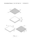
[0009] FIG. 1 shows a flowchart of one embodiment of a method of making current collector.
[0010] FIG. 2 shows a Scanning Electron Microscope (SEM) image of one embodiment of a carbon nanotube film in the method of FIG. 1.
[0011] FIG. 3 shows a SEM image of one embodiment of a carbon nanotube layer.
[0012] FIG. 4 shows a flowchart of one embodiment of electroplating metal layer on the carbon nanotube layer.
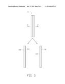
[0013] FIG. 5 shows a flowchart of one embodiment of dividing a carbon nanotube composite layer in the method of FIG. 1.
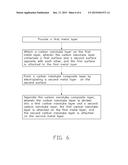
[0014] FIG. 6 shows a flowchart of another embodiment of a method of making current collector.
DETAILED DESCRIPTION
[0015] The disclosure is illustrated by way of example and not by way of limitation in the figures of the accompanying drawings in which like references indicate similar elements. It should be noted that references to "another," "an," or "one" embodiment in this disclosure are not necessarily to the same embodiment, and such references mean at least one.
[0016] Referring to FIG. 1, one embodiment of a method of making current collector 10 comprises:
[0017] step (S10), providing a carbon nanotube layer 110, wherein the carbon nanotube layer 110 comprises a first surface 111 and a second surface 113 opposite to each other;
[0018] step (S11), forming a carbon nanotube composite layer 11 via electroplating a first metal layer 120 on the first surface 111 and electroplating a second metal layer 130 on the second surface 113; and
[0019] step (S12), forming a first carbon nanotube layer 114 and a second carbon nanotube layer 116 by separating the carbon nanotube composite layer 11, wherein the first carbon nanotube layer 114 is attached on the first metal layer 120, and the second carbon nanotube layer 116 is attached on the second metal layer 130.
[0020] In step (S10), the carbon nanotube layer 110 can be located on a support (not shown). Furthermore, the carbon nanotube layer 110 can be suspended on a frame (not shown). The carbon nanotube layer 110 is a free-standing structure, and the carbon nanotube layer 110 can be suspended on the support or the frame.
[0021] The carbon nanotube layer 110 comprises a plurality of carbon nanotube films stacked together. Referring to FIG. 3, each of the plurality of carbon nanotube films comprises a plurality of carbon nanotubes. The plurality of carbon nanotubes that can be arranged substantially parallel to a surface of the carbon nanotube film. A large number of the carbon nanotubes in the carbon nanotube film can be oriented along a preferred orientation, meaning that a large number of the carbon nanotubes in the carbon nanotube film are arranged substantially along the same direction. An end of one carbon nanotube is joined to another end of an adjacent carbon nanotube arranged substantially along the same direction, by Van der Waals attractive force. A small number of the carbon nanotubes may be randomly arranged in the carbon nanotube film, and has a small if not negligible effect on the larger number of the carbon nanotubes in the carbon nanotube film arranged substantially along the same direction. The carbon nanotube film is capable of forming a free-standing structure. The term "free-standing structure" can be defined as a structure that does not have to be supported by a substrate. For example, a free standing structure can sustain the weight of itself when it is hoisted by a portion thereof without any significant damage to its structural integrity. So, if the carbon nanotube film is placed between two separate supporters, a portion of the carbon nanotube film, not in contact with the two supporters, would be suspended between the two supporters and yet maintain film structural integrity.
[0022] The plurality of carbon nanotubes in different carbon nanotube films can be intersected with each other. Thus the plurality of carbon nanotube films forms a network. A plurality of apertures 112 are defined in the carbon nanotube layer 110. The plurality of apertures 112 are through holes along the thickness of the carbon nanotube layer 110. In one embodiment, the carbon nanotube layer is suspended on the frame.
[0023] In step (S11), the first metal layer 120 is deposited on the first surface 111 via electroplating method. The second metal layer 130 is deposited on the second surface 113. The first metal layer 120 and the second metal layer 130 can be formed by:
[0024] step (S111), providing a metal ions solution, wherein the metal ions solution comprises a plurality of metal ions;
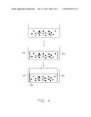
[0025] step (S112), immersing the carbon nanotube layer 110 into the metal ions solution, wherein the first surface 111 and the second surface 113 are exposed to the metal ions solution, and the carbon nanotube layer 110 is spaced from a electrode plate 140; and
[0026] step (S113), applying a voltage between the carbon nanotube layer 110 and the electrode plate 140, wherein the plurality of metal ions are reduced into metal particles and coated on the first surface 111 and the second surface 113.
[0027] In step (S111), the density of the plurality of metal ions can be selected according to the thickness of the first metal layer 120 and the second metal layer 130. In one embodiment, the plurality of metal ions are formed by dissolving cooper sulfate into the water.
[0028] In step (S112), the carbon nanotube layer 110 is spaced from the electrode plate 140. A distance between the carbon nanotube layer 110 and the electrode plate 140 can range from about 0.5 millimeters to about 3 millimeters. The carbon nanotube layer 110 can be parallel with the electrode plate 140. The material of the electrode plate 140 can be graphene, platinum, stainless steel, or carbon nanotube layer structure. The material of the electrode plated 140 can be inertia material in the metal ions solution. The size of the electrode plate 140 can be greater than the carbon nanotube layer.
[0029] The carbon nanotube layer 140 can be suspended in the metal ions solution. Furthermore, because the carbon nanotube layer 140 is fixed on the frame, the carbon nanotube layer 140 in the frame will be exposed to the metal ions solution. In one embodiment, the electrode plate 140 is copper plate, and the size of the copper plate is greater than the carbon nanotube layer 110.
[0030] In step (S113), a potential difference is applied between the carbon nanotube layer 110 and the electrode plate 140. The electrode plate 140 is electrically connected to a positive electrode, and the carbon nanotube layer 110 is electrically connected to a negative electrode. Thus the metal ions will be reduced into metal particles, and the metal particles will be deposited on the carbon nanotube layer 110. Furthermore, the metal particles are deposited on an outer surface of each of the plurality of carbon nanotubes. During the process of electroplating, a plurality of dangling bonds are formed on the outer surface of the plurality of carbon nanotubes, and the metal particles are tightly combined with the plurality of carbon nanotubes via the plurality of dangling bonds. Furthermore, the plurality of metal particles are connected with each other to form a continuous layered structure on the first surface 111 and the second surface 113. Thus both the first metal layer 120 and the second metal layer 130 are continuously layered structure. In addition, the metal particles can be deposited on the outer surface of adjacent carbon nanotubes around each of the plurality of apertures 112. Thus the first metal layer 120 and the second metal layer 130 are combined together to form an integrated structure. The carbon nanotube layer 110 is firmly sandwiched between the first metal layer 120 and the second metal layer 130.
[0031] In one embodiment, a constant voltage is applied between the carbon nanotube layer 110 and the electrode plate 140. The potential difference between the carbon nanotube layer 110 and the electrode plate 140 ranges from about 0.5 V to about 1.2 V, and an electroplating time range from about 0.5 hours to about 4 hours.
[0032] Furthermore, the first metal layer 120 and the second metal layer 130 can be formed one after another. In one embodiment, the second surface 113 can be attached on a substrate (not shown), and the first surface 111 is exposed in the metal ion solution. The first metal layer 120 can be formed on the first surface 111. The carbon nanotube layer 110 with the first metal layer 120 is turned over, and the second surface 113 is exposed in the metal ion solution. The second metal layer 130 is formed on the second surface 113.
[0033] Furthermore, during forming the second metal layer 130, the metal particles can be deposited into the plurality of apertures 112. Thus the second metal layer 130 can penetrate the carbon nanotube layer 110 and combined with the first metal layer 120 through the plurality of apertures 112. The carbon nanotube layer 110 is sandwiched between the first metal layer 120 and the second metal layer 130.
[0034] Furthermore, the carbon nanotube composite layer 11 can be washed to remove the impurity. Then the carbon nanotube composite layer 11 can be dried, and the first metal layer 120 and the second metal layer 130 can be tightly attached on the carbon nanotube layer 110.
[0035] In step (S12), the carbon nanotube composite layer 11 can be split apart by applying two opposite forces on two opposite surface of the carbon nanotube composite layer 11. Referring to FIG. 5, the carbon nanotube composite layer 11 can be separated apart by:
[0036] step (S121), applying a first force F on one surface of the carbon nanotube composite layer 11, and applying a second force F' on the other surface of the carbon nanotube composite layer 11, wherein the first force F is opposite to the second force F'; and
[0037] step (S122), separating the carbon nanotube composite layer 11 by continuously applying the first force F and the second force F', wherein the carbon nanotube layer 110 is divided into the first carbon nanotube layer 114 and the second carbon nanotube layer 116, the first metal layer 120 is attached on the first carbon nanotube layer 114, and the second metal layer 130 is attached on the second carbon nanotube layer 116.
[0038] In step (S121), the first force F and the second force F' can be selected according to the thickness of the carbon nanotube layer 110, to ensure that the carbon nanotube layer 110 can be divided into the first carbon nanotube layer 114 and the second carbon nanotube layer 116 along the direction of the thickness. Furthermore, the carbon nanotube layer 110 can be split along a central plane between the first surface and the second surface. The first force F and the second force F' can be applied on the two opposite surfaces of the carbon nanotube layer 110. The first force F and the second force F' can be applied along a straight line perpendicular to the carbon nanotube layer 110. The first carbon nanotube layer 114, the second carbon nanotube layer 116, and the carbon nanotube layer 110 have substantially the same size. Thus the two current collectors 10 can have the same size.
[0039] The first force F and the second force F' can be applied by attaching two adhesive tapes on the first metal layer 120 and the second metal layer 130, and pulling the two adhesive tapes to separate the carbon nanotube layer 110. Furthermore, the first force F and the second force F' can be applied through nippers. In one embodiment, the carbon nanotube layer 110 can also be divided by cutting the carbon nanotube layer 11 during applying the first force F and the second force F'. Furthermore, the first metal layer 120 can be fixed, and the second metal layer 130 is applied with the second force F' to separate the carbon nanotube layer 110.
[0040] In step (S122), the carbon nanotube layer 110 is divided into the first carbon nanotube layer 114 and the second carbon nanotube layer 116 by continuously applying the first force F and the second force F'. Furthermore, the first metal layer 120 is combined with the first carbon nanotube layer 114, and the second metal layer 130 is combined with the second carbon nanotube layer 116. In addition, the first carbon nanotube layer 114 and the second carbon nanotube layer 116 have the same thickness. The plurality of carbon nanotubes in the fist carbon nanotube layer 114 are parallel with the surface of the first metal layer 120. The plurality of carbon nanotubes in the second carbon nanotube layer 116 are parallel with surface of the second metal layer 130.
[0041] The method of making current collector has following advantages. The first metal layer and the second metal layer are formed on the carbon nanotube layer via electroplating method, thus the first metal layer and the second metal layer can be bonded on the carbon nanotube layer, and the carbon nanotubes can be tightly combined with the metal layer. Furthermore, the corruption to the metal layer caused by the electrolyte can be reduced or blocked by the carbon nanotube layer, thus the affection caused by the corruption can be reduced. The carbon nanotube layer has great conductivity, thus the carbon nanotube layer can be electrically connected to the electrode, and the resistance between the current collector and the active material in the electrode can be reduced. The two current collectors can be obtained by separating apart the first metal layer and the second metal layer, and the production efficiency is high.
[0042] Referring to FIG. 6, another embodiment of a method of making current collector 10 comprises:
[0043] step (S20), providing a first metal layer 120;
[0044] step (S21), attaching a carbon nanotube layer 110 on the first metal layer 120, wherein the carbon nanotube layer 110 comprises a first surface 111 and a second surface 113 opposite with each other, and the first surface 111 is attached to the first metal layer 120;
[0045] step (S22), forming a carbon nanotube composite layer 11 by electroplating a second metal layer 130 on the second surface 113; and
[0046] step (S23), separating the carbon nanotube composite layer 11, wherein the carbon nanotube layer 110 is divided into a first carbon nanotube layer 114 and a second carbon nanotube layer 116, the first carbon nanotube layer 114 is attached on the first metal layer 120, and the second carbon nanotube layer 116 is attached on the second metal layer 130.
[0047] The method of making current collector 10 in this embodiment is similar with the method of making current collector 10 in the embodiment described above, except that the carbon nanotube layer 110 is firstly attached on the first metal layer 120, and the second metal layer 130 is then electroplated on the carbon nanotube layer 110 and combined with the first metal layer 120.
[0048] In step (S21), the first metal layer 120 can be tightly combined with the carbon nanotube layer 110 and support the carbon nanotube layer 110. In one embodiment, a thickness of the metal layer 120 is about 10 micrometers. Thus the first metal layer 120 has certain mechanical strength.
[0049] In step (S22), during the process of the depositing the second metal layer 130, the second metal layer 130 will be penetrate the carbon nanotube layer 110 through the plurality of apertures 112 in the carbon nanotube layer 110. Thus the second metal layer 130 will be integrated with the first metal layer 120 to form an integrated structure. The carbon nanotube layer 110 is firmly sandwiched between the first metal layer 120 and the second metal layer 130.
[0050] Depending on the embodiment, certain steps of methods described may be removed, others may be added, and the sequence of steps may be altered. It is also to be understood that the description and the claims drawn to a method may include some indication in reference to certain steps. However, the indication used is only to be viewed for identification purposes and not as a suggestion as to an order for the steps.
[0051] Finally, it is to be understood that the above-described embodiments are intended to illustrate rather than limit the present disclosure. Variations may be made to the embodiments without departing from the spirit of the present disclosure as claimed. Elements associated with any of the above embodiments are envisioned to be associated with any other embodiments. The above-described embodiments illustrate the scope of the present disclosure but do not restrict the scope of the present disclosure.
User Contributions:
Comment about this patent or add new information about this topic:
Images included with this patent application:
 |  |
 |  |
 |  |
 |
| Similar patent applications: | |
| Date | Title |
|---|---|
| 2016-04-28 | Method of detecting test substance |
| 2015-10-29 | Reactor and method for activating reactor |
| 2015-12-24 | Cathodic protection management system |
| 2016-05-05 | Recovery of tritium from molten lithium blanket |
| 2016-05-12 | Forming method of thermal insulation film |
| New patent applications in this class: | |
| Date | Title |
|---|---|
| 2012-12-27 | Method for depositing a metal onto a porous carbon layer |
| 2012-05-10 | Composite electrode and method for manufacturing the same |
| 2011-04-14 | Electrode for lead-acid battery and method for producing such an electrode |
| New patent applications from these inventors: | |
| Date | Title |
|---|---|
| 2022-08-18 | Method for designing nonsymmetric freeform surface optical system |
| 2022-08-11 | Method for designing freeform concave grating imaging spectrometer |
| 2022-08-11 | Nonsymmetric freeform surface optical system |
| 2022-08-04 | Lithium metal anode and method for making the same |
| 2022-07-28 | Method of testing an oxidation potential of an electrolyte |
| Top Inventors for class "Electrolysis: processes, compositions used therein, and methods of preparing the compositions" | |
| Rank | Inventor's name |
|---|---|
| 1 | Benjamin J. Feldman |
| 2 | Adam Heller |
| 3 | Michael S. Lockard |
| 4 | Fei Mao |
| 5 | Joseph A. Vivolo |