Patent application title: METHOD FOR MANUFACTURING THIN FILM TRANSISTOR, AND THIN FILM TRANSISTOR THEREOF
Inventors:
Zongze He (Beijing, CN)
Assignees:
BEIJING BOE DISPLAY TECHNOLOGY CO., LTD.
BOE TECHNOLOGY GROUP CO., LTD.
IPC8 Class: AH01L29786FI
USPC Class:
257 57
Class name: Non-single crystal, or recrystallized, semiconductor material forms part of active junction (including field-induced active junction) amorphous semiconductor material field effect device in amorphous semiconductor material
Publication date: 2014-05-15
Patent application number: 20140131712
Abstract:
The present invention relates to the field of liquid crystal display, and
provides a method for manufacturing a TFT and the TFT thereof. The TFT
comprises: a substrate; a gate electrode with a three-dimensional
structure formed on the substrate; a gate insulating layer for covering
the gate electrode; a semiconductor layer formed on the gate insulating
layer; a buffer layer formed on the semiconductor layer; and source and
drain electrodes formed on the buffer layer, wherein the semiconductor
layer of the TFT is of a three-dimensional structure. According to the
present invention, it is able to reduce the driving voltage, the power
consumption of the driving circuit and the area occupied by the TFT, and
to increase the light transmission rate.Claims:
1. A method for manufacturing a TFT (Thin Film Transistor), comprising
the steps of: providing a substrate; forming a gate electrode with a
three-dimensional structure on the substrate; forming a gate insulating
layer for covering the gate electrode on the substrate on which the gate
electrode is formed; forming a semiconductor layer on the substrate on
which the gate insulating layer is formed; forming a buffer layer on the
substrate on which the semiconductor layer is formed; and forming a metal
layer on the substrate on which the buffer layer is formed, and treating
the metal layer by a patterning process to form source and drain
electrodes, wherein the semiconductor layer of the TFT is of a
three-dimensional structure.
2. The method according to claim 1, wherein the three-dimensional structure of the gate electrode is a cuboid or cube.
3. The method according to claim 1, wherein the three-dimensional structure of the semiconductor layer is an inverted-U slot structure covering the gate electrode.
4. The method according to claim 3, wherein a portion of the semiconductor layer between the source and drain electrodes forms a channel, a length of the channel is the distance between the source and drain electrodes, and a width of the channel≧(a width of the gate electrode+2*a height of the gate electrode).
5. The method according to claim 2, wherein the step of forming a gate electrode with a three-dimensional structure on the substrate comprises: depositing a first metal layer on the substrate; and treating the first metal layer by a patterning process to form the gate electrode with a three-dimensional structure.
6. The method according to claim 5, wherein the first metal layer can be made of ITO, or a metal selected from the group consisting of Cr, Mo, Al, Nd, Mo, W, Ti, Ta and Cu, or an alloy thereof.
7. The method according to claim 2, wherein the step of forming a gate insulating layer for covering the gate electrode on the substrate on which the gate electrode is formed comprises: depositing an insulating material layer on the substrate on which the gate electrode with a cuboid structure is formed; and treating the insulating material layer by a patterning process to form the gate insulating layer on a top face and two side faces of the gate electrode.
8. The method according to claim 2, wherein the step of forming a semiconductor layer on the substrate on which the gate insulating layer comprises: depositing a semiconductor material layer on the substrate on which the gate insulating layer is formed; and treating the semiconductor material layer by a patterning process to form the semiconductor layer on the gate insulating layer.
9. The method according to claim 2, wherein the step of forming a buffer layer on the substrate on which the semiconductor layer is formed comprises: depositing an N+ amorphous silicon material layer on the substrate on which the semiconductor layer is formed; and treating the N+ amorphous silicon material layer by a patterning process to form the buffer layer on the semiconductor layer.
10. The method according to claim 2, wherein the step of forming a metal layer on the substrate on which the buffer layer is formed and treating the metal layer by a patterning process to form source and drain electrodes comprises: depositing a second metal layer on the substrate on which the buffer layer is formed; and treating the second metal layer by a patterning process to form the source and drain electrodes on the buffer layer.
11. The method according to claim 10, wherein the second metal layer can be made of a metal selected from the group consisting of Cr, Mo, Al, Nd, Mo, W, Ti, Ta and Cu, or an alloy thereof.
12. A TFT (Thin Film Transistor), comprising: a substrate; a gate electrode with a three-dimensional structure formed on the substrate; a gate insulating layer for covering the gate electrode; a semiconductor layer formed on the gate insulating layer; a buffer layer formed on the semiconductor layer; and source and drain electrodes formed on the buffer layer, wherein the semiconductor layer of the TFT is of a three-dimensional structure.
13. The TFT according to claim 12, wherein the three-dimensional structure of the gate electrode is a cuboid or cube.
14. The TFT according to claim 12, wherein the three-dimensional structure of the semiconductor layer is an inverted-U slot structure covering the gate electrode.
15. The TFT according to claim 13, wherein a portion of the semiconductor layer between the source and drain electrodes forms a channel, a length of the channel is the distance between the source and drain electrodes, and a width of the channel≧(a width of the gate electrode+2*a height of the gate electrode).
16. The TFT according to claim 15, wherein the channel of the TFT at least comprises three electronic gates.
Description:
CROSS REFERENCE
[0001] The present application claims a priority of the Chinese patent application No. 201210460335.2 filed on Nov. 15, 2012, which is incorporated herein by reference in its entirety.
TECHNICAL FIELD
[0002] The present invention relates to the field of liquid crystal display, in particular to a method for manufacturing a thin film transistor and the thin film transistor thereof.
BACKGROUND
[0003] In the field of display, flat-panel displays with high PPI (Pixels per inch) values have become a key competition for manufacturers. However, when the panel has a high PPI value, a number of issues in, for example, power consumption and light transmission will occur. As a result, it has become a technical problem to increase a saturation current and ensure a certain charging rate by increasing the channel width in the case of a reduced opaque area for a TFT (Thin Film Transistor) array substrate.
[0004] For the existing TFT array substrate, its channel and gate electrode layer are of a flat structure as a film, so it is impossible to fully and reasonably utilize a spatial volume to increase the saturation current.
SUMMARY
[0005] An object of the present invention is to provide a method for manufacturing a TFT and the TFT thereof, so as to reduce, to some extent, the driving voltage, the power consumption of the driving circuit and the area occupied by the TFT, and to increase the light transmission rate.
[0006] In one aspect, the present invention provides a method for manufacturing a TFT, comprising the steps of :
[0007] providing a substrate;
[0008] forming a gate electrode with a three-dimensional structure on the substrate;
[0009] forming a gate insulating layer for covering the gate electrode on the substrate on which the gate electrode is formed;
[0010] forming a semiconductor layer on the substrate on which the gate insulating layer is formed;
[0011] forming a buffer layer on the substrate on which the semiconductor layer is formed; and
[0012] forming a metal layer on the substrate on which the buffer layer is formed, and treating the metal layer by a patterning process to form source and drain electrodes,
[0013] wherein the semiconductor layer of the TFT is of a three-dimensional structure.
[0014] Preferably, the three-dimensional structure of the gate electrode is a cuboid or cube.
[0015] The three-dimensional structure of the semiconductor layer is an inverted-U slot structure covering the gate electrode.
[0016] A portion of the semiconductor layer between the source and drain electrodes forms a channel. A length of the channel is the distance between the source and drain electrodes, and a width of the channel≧(a width of the gate electrode+2*a height of the gate electrode).
[0017] The step of forming a gate electrode with a three-dimensional structure on the substrate comprises:
[0018] depositing a first metal layer on the substrate; and
[0019] treating the first metal layer by a patterning process to form the gate electrode with a three-dimensional structure.
[0020] The first metal layer may be made of ITO, or a metal selected from the group consisting of Cr, Mo, Al, Nd, Mo, W, Ti, Ta and Cu or an alloy thereof.
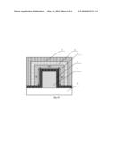
[0021] The step of forming a gate insulating layer for covering the gate electrode on the substrate on which the gate electrode is formed comprises:
[0022] depositing an insulating material layer on the substrate on which the gate electrode with a cuboid structure is formed; and
[0023] treating the insulating material layer by a patterning process to form the gate insulating layer on a top face and two side faces of the gate electrode.
[0024] The step of forming a semiconductor layer on the substrate on which the gate insulating layer comprises:
[0025] depositing a semiconductor material layer on the substrate on which the gate insulating layer is formed; and
[0026] treating the semiconductor material layer by a patterning process to form the semiconductor layer on the gate insulating layer.
[0027] The step of forming a buffer layer on the substrate on which the semiconductor layer is formed comprises:
[0028] depositing an N+ amorphous silicon material layer on the substrate on which the semiconductor layer is formed; and
[0029] treating the N+ amorphous silicon material layer by a patterning process to form the buffer layer on the semiconductor layer.
[0030] The step of forming a metal layer on the substrate on which the buffer layer is formed and treating the metal layer by a patterning process to form source and drain electrodes comprises:
[0031] depositing a second metal layer on the substrate on which the buffer layer is formed; and
[0032] treating the second metal layer by a patterning process to form the source and drain electrodes on the buffer layer.
[0033] The second metal layer may be made of a metal selected from the group consisting of Cr, Mo, Al, Nd, Mo, W, Ti, Ta and Cu or an alloy thereof.
[0034] In another aspect, the present invention further provides a TFT, comprising:
[0035] a substrate;
[0036] a gate electrode with a three-dimensional structure formed on the substrate;
[0037] a gate insulating layer for covering the gate electrode;
[0038] a semiconductor layer formed on the gate insulating layer;
[0039] a buffer layer formed on the semiconductor layer; and
[0040] source and drain electrodes formed on the buffer layer,
[0041] wherein the semiconductor layer of the TFT is of a three-dimensional structure.
[0042] Preferably, the three-dimensional structure of the gate electrode is a cuboid or cube.
[0043] The three-dimensional structure of the semiconductor layer is an inverted-U slot structure covering the gate electrode.
[0044] A portion of the semiconductor layer between the source and drain electrodes forms a channel. A length of the channel is the distance between the source and drain electrodes, and a width of the channel≧(a width of the gate electrode+2*a height of the gate electrode).
[0045] The channel of the TFT at least includes three electronic gates.
[0046] The above technical solutions of the present invention have the following beneficial effect.
[0047] According to solutions of the present invention, the number of the electronic gates will be increased due to the use of a TFT with a three-dimensional structure, that is, in the case of an identical gate voltage and an identical area occupied by the TFT, the TFT of the present invention has a saturation current larger than that of a traditional flat TFT. As a result, it is able to reduce, to some extent, the driving voltage, the power consumption of the driving circuit and the area occupied by the TFT, and to increase the light transmission rate.
BRIEF DESCRIPTION OF THE DRAWINGS
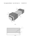
[0048] FIG. 1 is a schematic view showing the structure of a TFT according to embodiments of the present invention; and
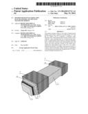
[0049] FIGS. 2-10 are schematic views showing a method for manufacturing a TFT according to embodiments of the present invention.
DETAILED DESCRIPTION
Embodiment 1
[0050] As shown in FIGS. 2-10, the embodiment of the present invention provides a method for manufacturing a TFT, comprising:
[0051] Step 1: providing a substrate 11;
[0052] Step 2: forming a gate electrode with a three-dimensional structure on the substrate 11;
[0053] Step 3: forming a gate insulating layer for covering the gate electrode on the substrate on which the gate electrode is formed;
[0054] Step 4: forming a semiconductor layer on the substrate on which the gate insulating layer is formed;
[0055] Step 5: forming a buffer layer on the substrate on which the semiconductor layer is formed; and
[0056] Step 6: forming a metal layer on the substrate on which the buffer layer is formed, and treating the metal layer by a patterning process to form source and drain electrodes, wherein the semiconductor layer of the TFT is of a three-dimensional structure.
[0057] According to the embodiment of the present invention, the number of corresponding electronic gates are increased by forming a TFT with a three-dimensional structure on the substrate, that is, the TFT of the present invention has a saturation current larger than that of a traditional flat TFT in the case of an identical gate voltage and an identical area occupied by the TFT. As a result, it is able to reduce, to some extent, the driving voltage, the power consumption of the driving circuit and the area occupied by the TFT, and to increase the light transmission rate.
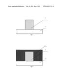
[0058] As shown in FIGS. 2 and 3, Step 2 comprises:
[0059] Step 21: depositing a first metal layer 1' on the substrate; and
[0060] Step 22: treating the first metal layer 1' by a patterning process to form a gate electrode 1 with a three-dimensional structure, wherein the three-dimensional structure is a cuboid.
[0061] The first metal layer 1' may be made of ITO, or a metal selected from the group consisting of Cr, Mo, Al, Nd, Mo, W, Ti, Ta and Cu, or an alloy thereof.
[0062] An existing gate electrode is of a film structure with a very small thickness, while the gate electrode 1 of the present invention is of a three-dimensional structure with a thickness larger than a film. Preferably, the gate electrode 1 has a shape of cuboid. Other structures may be further provided on the basis of the gate electrode 1 having the shape of cuboid so that the entire TFT has a cuboid structure. It should be noted that, cuboid is merely a preferred shape for the TFT so as to facilitate the production and machining, and the TFT may also be a cube or any other shapes with a cross section of trapezoid or arch, as if it has a saturation current larger than a traditional flat TFT with a flat structure as a film in the case of an identical gate voltage and an identical area occupied by the TFT.
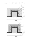
[0063] As shown in FIGS. 4 and 5, Step 3 comprises:
[0064] Step 31: depositing an insulating material layer 2' on the substrate 11 on which the gate electrode 1 with a cuboid structure is formed (as shown in FIG. 4); and
[0065] Step 32: treating the insulating material layer 2' by a patterning process to form the gate insulating layer 2 on a top face and two side faces of the gate electrode 1 (as shown in FIG. 5), wherein the gate insulating layer 2 may be made of oxides, nitrides or nitrogen oxides, such as SiNx.
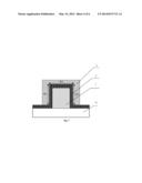
[0066] As shown in FIGS. 6 and 7, Step 4 comprises:
[0067] Step 41: depositing a conductive material layer 3' on the substrate 11 on which the gate insulating layer 2 is formed (as shown in FIG. 6); and
[0068] Step 42: treating the conductive material layer 3' by a patterning process to form the semiconductor layer 3 on the gate insulating layer 2 (as shown in FIG. 7), wherein the three-dimensional structure of the semiconductor layer 3 is an inverted-U slot structure covering the gate electrode 1 (here, the structure of the semiconductor layer 3 is not limited, as if it covers the gate electrode and has the structure corresponding to that of the gate electrode), and the semiconductor layer 3 may be made of a-Si.
[0069] As shown in FIGS. 8 and 9, Step 5 comprises:
[0070] Step 51: depositing an N+ amorphous silicon material layer 4' on the substrate 11 on which the semiconductor layer 3 is formed (as shown in FIG. 8); and
[0071] Step 52: treating the N+ amorphous silicon material layer 4' (such as N+ a-Si) by a patterning process to form the buffer layer 4 on the semiconductor layer 3 (as shown in FIG. 9), wherein the buffer layer 4 may be a doped or a non-doped semiconductor layer.
[0072] As shown in FIG. 10, Step 6 comprises:
[0073] Step 61: depositing a second metal layer on the substrate 11 on which the buffer layer 4 is formed; and
[0074] Step 62: treating the second metal layer by a patterning process to finally form the source and drain electrodes 5 on the buffer layer 4 (as shown in FIG. 10), wherein the second metal layer may be made of a metal selected from the group consisting of Cr, Mo, Al, Nd, Mo, W, Ti, Ta and Cu, or an alloy thereof.
[0075] FIG. 1 is a three-dimensional view showing the structure of the TFT with a three-dimensional structure finally obtained through the above-mentioned steps.
[0076] As show in FIG. 7, the three-dimensional structure of the semiconductor layer 3 may be an inverted-U slot structure covering the gate electrode, Due to this structure, the semiconductor layer 3 has three planes. A conductive channel will be formed in these planes during the operation of the TFT, so these planes constitute conductive gates, i.e., three electronic gates.
[0077] A portion of the semiconductor layer 3 between the source and drain electrodes forms a channel. A length of the channel is the distance between the source and drain electrodes. A width W of the channel≧(W1+W2+W3). W1 and W3 each represents a height of the gate electrode, and W2 represents a width of the gate electrode. As compared to the channel (with a width such as W2) for an existing flat structure, W is obviously greater than W2. Hence, according to the TFT of the present invention with a three-dimensional structure, the effective channel width is increased remarkably, so that the number of the electronic gates is increased correspondingly, e.g., at least three electronic gates. The TFT of the present invention has a saturation current greater than that of a traditional flat TFT in the case of an identical gate voltage and an identical area occupied by the TFT. As a result, it is able to reduce, to some extent, the driving voltage, the power consumption of the driving circuit and the area occupied by the TFT, and to increase the light transmission rate.
[0078] According to the equation
I saturation = W L K ( V GS - V TH ) 2 , ##EQU00001##
it can be seen that the saturation current will increase along with the channel width. In the equation, W represents a channel width, VGS represents a voltage of the gate electrode 1 relative to the semiconductor layer 3, VTH represents a minimum voltage desired for the induction of a carrier, K represents a Boltzmann constant, and L represents an effective channel length. As a result, it is able to reduce, to some extent, the driving voltage, the power consumption of the driving circuit and the area occupied by the TFT, and to increase the light transmission rate.
Embodiment 2
[0079] As shown in FIGS. 1-10, the embodiment of the present invention provides a TFT, comprising: a substrate; a gate electrode 1 with a three-dimensional structure formed on the substrate; a gate insulating layer 2 for covering the gate electrode; a semiconductor layer 3 formed on the gate insulating layer 2; a buffer layer 4 formed on the semiconductor layer 3; and source and drain electrodes 5 formed on the buffer layer 4. A channel formed on the TFT is of a three-dimensional structure, e.g., a cuboid as shown in FIG. 1. The channel of the TFT at least comprises three electronic gates.
[0080] Other structures may be further provided on the basis of the gate electrode 1 with a cuboid structure so that the entire TFT also has a cuboid structure. It should be noted that, cuboid is merely a preferred shape for the TFT so as to facilitate the production and machining, and the TFT may also be a cube or any other shapes, as if it has a saturation current larger than a traditional flat TFT with a flat structure as a film in the case of an identical gate voltage and an identical area occupied by the TFT.
[0081] The TFT has a three-dimensional structure, so the number of the electronic gates may be increased, that is, the TFT has a saturation current greater than that of a traditional flat TFT in the case of an identical gate voltage and an identical area occupied by the TFT. According to the equation Isaturation=W/LK(VGS-VTH)2, it can be seen that the saturation current will increase along with the channel width. In the equation, W represents a channel width, VGS represents a voltage of the gate electrode 1 relative to the semiconductor layer 3, VTH represents a minimum voltage desired for the induction of a carrier, K represents a Boltzmann constant, and L represents an effective channel length. As a result, it is able to reduce, to some extent, the driving voltage, the power consumption of the driving circuit and the area occupied by the TFT, and to increase the light transmission rate.
[0082] The above are merely the preferred embodiments of the present invention. It should be noted that, a person skilled in the art may make improvements and modifications without departing from the principle of the present invention, and these improvements and modifications shall also be considered as the scope of the present invention.
User Contributions:
Comment about this patent or add new information about this topic:
Images included with this patent application:
 |  |
 |  |
 |  |
 |
| New patent applications in this class: | |
| Date | Title |
|---|---|
| 2016-07-07 | Field-effect transistor and semiconductor device |
| 2016-06-30 | Active element and fabricating method thereof |
| 2016-06-16 | Copper-alloy barrier layers for metallization in thin-film transistors and flat panel displays |
| 2015-12-17 | Metal gate stack structure and manufacturing method |
| 2015-12-03 | Fabrication of transistor with high density storage capacitor |
| New patent applications from these inventors: | |
| Date | Title |
|---|---|
| 2021-11-25 | Display device and driving method |
| 2021-11-04 | Backlight module, control method therefor and display device, driving method therefor |
| 2020-12-31 | Sub-pixel unit, display panel, and display apparatus and drive method therefor |
| 2016-01-07 | Image display controlling method and control device thereof, image display device |
| 2015-12-31 | Interface conversion circuit, display panel driving method and display apparatus |
| Top Inventors for class "Active solid-state devices (e.g., transistors, solid-state diodes)" | |
| Rank | Inventor's name |
|---|---|
| 1 | Shunpei Yamazaki |
| 2 | Shunpei Yamazaki |
| 3 | Kangguo Cheng |
| 4 | Huilong Zhu |
| 5 | Chen-Hua Yu |