Patent application title: METHOD FOR AFFIXING ADHESIVE FILMS AND MAIN BOARD WITH ADHESIVE FILMS APPLIED USING THE METHOD
Inventors:
Hua-Lin Lv (Shenzhen City, CN)
Kok-Kan Chan (Santa Clara, CA, US)
Ting-Jian Zou (Shenzhen City, CN)
Yu Zou (Shenzhen City, CN)
Kai-Gui Wang (Shenzhen City, CN)
Assignees:
HON HAI PRECISION INDUSTRY CO., LTD.
FU TAI HUA INDUSTRY (SHENZHEN) CO., LTD.
IPC8 Class: AH05K900FI
USPC Class:
361818
Class name: For electronic systems and devices shielding emi
Publication date: 2011-10-27
Patent application number: 20110261552
Abstract:
A method for affixing adhesive films to a main board is provided. The
main board includes a main body and a shield. The shield includes a first
shield and a second shield. The second shield defines openings. When the
second shield is attached to the main body, components of the main body
are confined within the openings, respectively. The method includes:
first absorbing a single adhesive film to an electrostatic absorbing
film. Then, stamping the electrostatic absorbing film and the single
adhesive film to form adhesive films that have substantially the same
shape and arrangement as the openings. Next, aligning the electrostatic
absorbing film with the first shield and affixing the adhesive films to
the first shield. Then, removing the electrostatic absorbing film from
the first shield. And, assembling the first shield to the second shield.Claims:
1. A method for affixing a plurality of adhesive films to a main board,
the main board comprising a main body and a shield, the shield comprising
a first shield and a second shield, the second shield defining a
plurality of openings, when the second shield being attached to the main
body, components of the main body being confined within the openings,
respectively, the method comprising: sticking a single adhesive film to
an electrostatic absorbing film; stamping the electrostatic absorbing
film and the single adhesive film stuck to the electrostatic absorbing
film to form the plurality of adhesive films that have substantially the
same shape and arrangement as the plurality of openings; aligning the
electrostatic absorbing film with the first shield and affixing the
plurality of adhesive films to the first shield; removing the
electrostatic absorbing film from the first shield; and assembling the
first shield to the second shield.
2. The method for affixing a plurality of adhesive films as described in claim 1, wherein the shape of the electrostatic absorbing film is substantially the same as the first shield.
3. The method for affixing a plurality of adhesive films as described in claim 1, wherein the electrostatic absorbing film is a PET release film.
4. The method for affixing a plurality of adhesive films as described in claim 1, wherein the adhesive films are made of insulating material.
5. A main board, comprising: a shield comprising a first shield and a second shield, the second shield defining a plurality of openings; a main body comprising a plurality of components, the second shield being attached to the main body, the plurality of components being confined within the plurality of openings of the second shield, respectively; and a plurality of adhesive films affixed to the first shield in such a way that the plurality of adhesive films and the plurality of openings are substantially the same in shape and arrangement, allowing the plurality of adhesive films to prevent the first shield from contacting the components within the plurality of openings of the second shield.
6. The main board as described in claim 5, wherein the adhesive films are made of insulating material.
Description:
BACKGROUND
[0001] 1. Technical Field
[0002] The present disclosure relates to adhesive films and, particularly, to a method for affixing adhesive films to a main board.
[0003] 2. Description of Related Art
[0004] A shield is usually used to protect a computer main board against static electricity and electromagnetic interference (EMI). Generally, the shield includes a first shield and a second shield stacked on each other. The second shield is fixed to the main board. To prevent the first shield from contacting the components of the main board, a layer of film is usually affixed to the main board. A method for efficiently affixing the film is thus desirable.
BRIEF DESCRIPTION OF THE DRAWINGS
[0005] The components of the drawings are not necessarily drawn to scale, the emphasis instead being placed upon clearly illustrating the principles of present disclosure. Moreover, in the drawings, like reference numerals designate corresponding parts throughout several views.
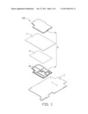
[0006] FIG. 1 is an exploded isometric view of a main board in accordance with an exemplary embodiment, showing a first state of the main board.
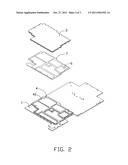
[0007] FIG. 2 is similar to FIG. 1, showing a second state of the main board.
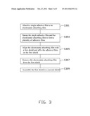
[0008] FIG. 3 is a flowchart of a method for affixing the adhesive films in accordance with an exemplary embodiment.
DETAILED DESCRIPTION
[0009] Referring to FIGS. 1-2, a main board 100 is shown. The main board 100 includes a main body 1 and a shield 2. The shield 2 includes a first shield 3 and a second shield 4 to protect against electromagnetic interference (EMI). In the embodiment, the second shield 4 is a frame defining a plurality of openings 40. After the second shield 4 is attached to the main body 1, corresponding components of the main body 1 are confined within the respective openings 40.
[0010] In the embodiment, to prevent the first shield 3 from contacting/damaging the components on the main body 1, a plurality of insulating, single-sided adhesive films 6 matching the respective openings 40 is provided. The adhesive films 6 are affixed to the first shield 3 in such a way that the arrangement of the adhesive films 6 is substantially the same as the openings 40, preventing the first shield 3 from contacting/damaging the components within the openings 40.
[0011] Referring to FIG. 3, a flowchart of a method for affixing adhesive films 6 is provided. In step S301, a single adhesive film 5 is provided and one side of the adhesive film 5 having no adhesive is stuck to an electrostatic absorbing film 7, such as a PET film. The non-adhesive side of the film 5 adheres to the PET film 7 because of the adherent nature of the surface of PET films.
[0012] In step S303, stamping the single adhesive film 5 and the electrostatic absorbing film 7 to form the adhesive films 6 on the electrostatic absorbing film 7. The machine (not shown) for the stamping has sufficient precision to cut the single adhesive film 5 into the plurality of adhesive films 6, with the electrostatic absorbing film 7 under the single adhesive film 5 left undamaged. After stamping, the electrostatic absorbing film 7 has substantially the same shape as the first shield 3. The arrangement and the shape of the adhesive films 6 are substantially the same as that of the openings 40 of the second shield 4.
[0013] In step S305, aligning the electrostatic absorbing film 7 with the first shield 3 and affixing the adhesive films 6 on the bottom of the first shield 3.
[0014] In step S307, removing the electrostatic absorbing film 7 from the first shield 3.
[0015] In step S309, assembling the first shield 3 to the second shield 4.
[0016] Although the present disclosure has been specifically described on the basis of the exemplary embodiment thereof, the disclosure is not to be construed as being limited thereto. Various changes or modifications may be made to the embodiment without departing from the scope and spirit of the disclosure.
User Contributions:
Comment about this patent or add new information about this topic:
Images included with this patent application:
 |  |
 |
| New patent applications in this class: | |
| Date | Title |
|---|---|
| 2016-06-16 | Formed channels providing electromagnetic shielding in electronics |
| 2016-04-28 | Display device |
| 2016-04-21 | Electronic apparatus and electromagnetic radiation suppression method |
| 2016-03-17 | Package structure |
| 2016-03-10 | Shield for acoustic device |
| New patent applications from these inventors: | |
| Date | Title |
|---|---|
| 2013-01-31 | Connecting assembly and electronic apparatus having same |
| 2012-01-26 | Switch assembly |
| 2011-12-01 | Electronic device and slide switch thereof |
| Top Inventors for class "Electricity: electrical systems and devices" | |
| Rank | Inventor's name |
|---|---|
| 1 | Zheng-Heng Sun |
| 2 | Levi A. Campbell |
| 3 | Li-Ping Chen |
| 4 | Robert E. Simons |
| 5 | Richard C. Chu |