Patent application title: TEMPERATURE COMPENSATION IN OUTPUT FEEDBACK OF A FLYBACK POWER CONVERTER
Inventors:
Ke-Chih Chou (Zhonghe City, TW)
Pei-Lun Huang (Zhubei City, TW)
Pei-Lun Huang (Zhubei City, TW)
Assignees:
RICHPOWER MICROELECTRONICS CORPORATION
IPC8 Class: AH03K3011FI
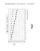
USPC Class:
327513
Class name: External effect temperature with compensation for temperature fluctuations
Publication date: 2011-01-27
Patent application number: 20110018609
Inventors list |
Agents list |
Assignees list |
List by place |
Classification tree browser |
Top 100 Inventors |
Top 100 Agents |
Top 100 Assignees |
Usenet FAQ Index |
Documents |
Other FAQs |
Patent application title: TEMPERATURE COMPENSATION IN OUTPUT FEEDBACK OF A FLYBACK POWER CONVERTER
Inventors:
PEI-LUN HUANG
KE-CHIH CHOU
Agents:
ROSENBERG, KLEIN & LEE
Assignees:
Origin: ELLICOTT CITY, MD US
IPC8 Class: AH03K3011FI
USPC Class:
Publication date: 01/27/2011
Patent application number: 20110018609
Abstract:
A secondary circuit of a flyback power converter has a resistor network to
monitor the output current of the flyback power converter, so as to
generate a voltage to apply to a base of a bipolar junction transistor to
thereby provide a collector signal for output feedback. The resistor
network has a temperature-dependent resistance to compensate the
temperature dependence of the base-emitter voltage imparted to the output
current and thereby stable the output current.Claims:
1. A secondary circuit of a flyback power converter including a capacitor
connected between an output end and a ground end to supply an output
current, and a secondary coil of a transformer to provide a secondary
current for charging the capacitor, the secondary circuit comprising:a
resistor network connected in a path of the output current to generate a
voltage according to the output current; anda bipolar junction transistor
having a base connected to the resistor network to receive the voltage
and providing a collector signal for output feedback;wherein the resistor
network has a resistance varying with temperature to compensate for a
temperature effect of a base-emitter voltage of the bipolar junction
transistor on the output current.
2. The secondary circuit of claim 1, wherein the resistor network comprises:a current sense resistor connected between the ground end and the capacitor; anda resistor and a thermistor connected in series to each other and connected in parallel to the current sense resistor.
3. A method for stabilizing an output current of a flyback power converter including a capacitor connected between an output end and a ground end to supply the output current, and a secondary coil of a transformer to provide a secondary current for charging the capacitor, the method comprising the steps of:generating a voltage by the output current flowing through a resistor network; andapplying the voltage to a base of a bipolar junction transistor to provide a collector signal for output feedback;wherein the resistor network has a resistance varying with temperature to compensate for a temperature effect of a base-emitter voltage of the bipolar junction transistor on the output current.
Description:
FIELD OF THE INVENTION
[0001]The present invention is related to power converters and, more particularly, to a circuit and method for temperature compensation in a secondary circuit of a flyback power converter.
BACKGROUND OF THE INVENTION
[0002]A bipolar junction transistor (BJT) typically has a base-emitter voltage (VBE) of 0.7V. However, as ambient temperature rises, VBE will decrease and thus may lead to system instability. Therefore, BJTs can only be used in a system capable of withstanding variation over a wide range and are avoided in certain circuits when designing a system where stable current is desired. For instance, if a BJT is used to reflect the output current of a flyback power converter to generate an output feedback, temperature variation may cause the output current to exceed a range set forth in the specification. While a switch-mode structure can be used to provide output current control and thereby enable a stable output current, the switch-mode structure is disadvantaged by a large number of components, a complicated and hard-to-control circuit, and high production costs. Therefore, the present invention provides a feedback control circuit and method with temperature compensation implemented by a BJT structure.
SUMMARY OF THE INVENTION
[0003]An object of the present invention is to provide a circuit and method for temperature compensation in a secondary circuit of a flyback power converter.
[0004]According to the present invention, a flyback power converter includes a capacitor connected between an output end and a ground end to supply an output current, and a transformer having a secondary coil to provide a secondary current for charging the capacitor. The flyback power converter has a secondary circuit which has a resistor network connected in a path of the output current to generate a voltage according to the output current, and a BJT having a base connected to the resistor network to receive the voltage and providing a collector signal for output feedback. The resistor network has a resistance varying with temperature to compensate for the temperature effect of the base-emitter voltage of the BJT on the output current.
[0005]According to the present invention, a method for stabilizing an output current of a flyback power converter includes generating a voltage by the output current flowing through a resistor network, and applying the voltage to a base of a BJT to provide a collector signal for output feedback. The resistor network has a resistance varying with temperature to compensate for the temperature effect of the base-emitter voltage of the BJT on the output current.
BRIEF DESCRIPTION OF THE DRAWINGS
[0006]These and other objects, features and advantages of the present invention will become apparent to those skilled in the art upon consideration of the following description of the preferred embodiments of the present invention taken in conjunction with the accompanying drawings, in which:
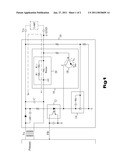
[0007]FIG. 1 is a circuit diagram of an embodiment according to the present invention; and
[0008]FIG. 2 is a plot showing the relationships between the output current and ambient temperature with and without temperature compensation.
DETAILED DESCRIPTION OF THE INVENTION
[0009]FIG. 1 is a circuit diagram of an embodiment according to the present invention, in which block 10 is the secondary circuit of a flyback power converter. The primary circuit of the flyback power converter includes a controller for switching a power switch to control a primary current of a transformer Tx to generate a secondary current for charging a capacitor C and thereby supplying a current Io for load. Output feedback is provided by an optical coupler 12 whose bias point is set by a shunt regulator 14. A constant current circuit 16 includes a current sense resistor Rsense connected between a ground end GND of the flyback power converter and the secondary coil of the transformer Tx to generate a voltage to be applied to a base B of a BJT 18. The BJT 18 has a collector connected to the optical coupler 12 to provide a collector signal thereto, to adjust the bias point of the optical coupler 12. In order to compensate for temperature-dependent variation of the base-emitter voltage VBE of the BJT 18, a resistor R1 and a thermistor RNTC are connected in series to each other and then connected in parallel to the current sense resistor Rsense to constitute a resistor network 20 having the equivalent resistance
RTOTAL=(R1+RNTC)/Rsense, [Eq-1]
and thereby
VBE=Io×RTOTAL. [Eq-2]
[0010]The thermistor RNTC has a negative temperature coefficient and thus, as ambient temperature rises, the voltage VBE falls down, but since the resistance RTOTAL decreases with the resistance of RNTC, the current
Io=VBE/RTOTAL [Eq-3]
remains stable. In other words, when VBE varies with temperature, RTOTAL varies accordingly and thereby compensates for the VBE-caused variation of the output current Io.
[0011]When ambient temperature varies, the resistance of the thermistor RNTC decreases fast. Therefore, in order to achieve fairly linear compensation and overcompensation, the resistor R1 is added to this embodiment and connected in series to the thermistor RNTC, before the resistor R1 and the thermistor RNTC are connected in parallel to the resistor Rsense. In other embodiments, the resistor network 20 may be so configured that the thermistor RNTC is connected in series to the current sense resistor Rsense or otherwise arranged, for the equivalent resistance RTOTAL to be negatively correlated to temperature, thus compensating for the negative correlation between the voltage VBE and temperature.
[0012]Table 1 shows experimental results with and without temperature compensation, and FIG. 2 is a plot based on the experimental results and showing the relationships between the output current Io and temperature. At room temperature (25° C.), the resistor Rsense has a resistance of 2Ω, the resistor R1 is set at 4.3Ω, and the thermistor RNTC is set at 10Ω. As shown clearly by the data of Table 1 and the curves of FIG. 2, the output current Io is more stable when the thermistor RNTC is used to provide temperature compensation. For example, when the operating temperature is 90° C., the output current Io obtained without RNTC is approximately 20.3% lower than that obtained under standard conditions; on the other hand, the output current Io obtained with RNTC is only 6.5% lower than that obtained under standard conditions, i.e., the approximately 20% drop-down of the output current Io is raised by nearly 14%.
TABLE-US-00001 TABLE 1 Output Current Io VBE RTOTAL Without RNTC With RNTC 30° C. 0.650 V 1.738 Ω 369 mA 370 mA 40° C. 0.637 V 1.699 Ω 350 mA 374 mA 50° C. 0.610 V 1.646 Ω 343 mA 368 mA 60° C. 0.585 V 1.603 Ω 331 mA 366 mA 70° C. 0.560 V 1.555 Ω 316 mA 361 mA 80° C. 0.538 V 1.512 Ω 307 mA 353 mA 90° C. 0.516 V 1.480 Ω 294 mA 346 mA
[0013]The temperature compensation circuit and method according to the present invention allow a BJT structure whose output current may otherwise vary over a wide range to provide stable constant current. After calculating the compensation abilities precisely, the disclosed circuit and method can be used to replace switch-mode structures which require complex control and high costs.
[0014]While the present invention has been described in conjunction with preferred embodiments thereof, it is evident that many alternatives, modifications and variations will be apparent to those skilled in the art. Accordingly, it is intended to embrace all such alternatives, modifications and variations that fall within the spirit and scope thereof as set forth in the appended claims.
User Contributions:
comments("1"); ?> comment_form("1"); ?>Inventors list |
Agents list |
Assignees list |
List by place |
Classification tree browser |
Top 100 Inventors |
Top 100 Agents |
Top 100 Assignees |
Usenet FAQ Index |
Documents |
Other FAQs |
User Contributions:
Comment about this patent or add new information about this topic:
Images included with this patent application:
 |  |
 |
| Similar patent applications: | |
| Date | Title |
|---|---|
| 2012-12-27 | Hybrid impedance compensation in a buffer circuit |
| 2010-10-21 | Temperature-compensated voltage comparator |
| 2008-11-13 | Method and apparatus for regulating power in a flyback converter |
| 2011-06-23 | Temperature compensation attenuator |
| 2012-02-09 | High temperature operating package and circuit design |
| New patent applications in this class: | |
| Date | Title |
|---|---|
| 2016-12-29 | Temperature stabilization of an on-chip temperature-sensitive element |
| 2016-06-23 | Temperature independent reference current generation for calibration |
| 2016-05-26 | Temperature compensation circuit, temperature compensation method and liquid crystal display |
| 2016-05-05 | Circuit and method for compensating for early effects |
| 2016-05-05 | Voice coil motor temperature sensing circuit to reduce catastrophic failure due to voice coil motor coil shorting to ground |
| New patent applications from these inventors: | |
| Date | Title |
|---|---|
| 2020-12-31 | Super-fast transient response (str) ac/dc converter for high power density charging application |
| 2017-02-16 | Flyback converter output current evaluation circuit and evaluation method |
| 2016-06-09 | Voltage detection circuit and a method of detecting voltage changes |
| 2016-06-09 | Methods and devices for detecting the input voltage and discharging the residuevoltage |
| 2012-01-19 | Power stage control circuit |
| Top Inventors for class "Miscellaneous active electrical nonlinear devices, circuits, and systems" | |
| Rank | Inventor's name |
|---|---|
| 1 | Yantao Ma |
| 2 | Feng Lin |
| 3 | Ming-Chieh Huang |
| 4 | Yong-Ju Kim |
| 5 | Chan-Hong Chern |