Patent application title: Method for forming fine patterns using etching slope of hard mask layer in semiconductor device
Inventors:
Sung-Yoon Cho (Kyoungki-Do, KR)
Hye-Ran Kang (Kyoungki-Do, KR)
IPC8 Class: AC23F104FI
USPC Class:
216 47
Class name: Etching a substrate: processes masking of a substrate using material resistant to an etchant (i.e., etch resist) mask is multilayer resist
Publication date: 2008-09-25
Patent application number: 20080230516
Inventors list |
Agents list |
Assignees list |
List by place |
Classification tree browser |
Top 100 Inventors |
Top 100 Agents |
Top 100 Assignees |
Usenet FAQ Index |
Documents |
Other FAQs |
Patent application title: Method for forming fine patterns using etching slope of hard mask layer in semiconductor device
Inventors:
Sung-Yoon Cho
Hye-Ran Kang
Agents:
BLAKELY SOKOLOFF TAYLOR & ZAFMAN LLP
Assignees:
Origin: SUNNYVALE, CA US
IPC8 Class: AC23F104FI
USPC Class:
216 47
Abstract:
A method for forming fine patterns in a semiconductor device includes
forming a first hard mask layer and a second hard mask layer over an etch
target layer, forming second hard mask patterns by etching the second
hard mask layer, wherein an etching profile of the second hard mask layer
has a positive slope, and etching the first hard mask layer and the etch
target layer using the second hard mask patterns as an etch mask.Claims:
1. A method for forming fine patterns in a semiconductor device, the
method comprising:forming a first hard mask layer and a second hard mask
layer over an etch target layer;forming second hard mask patterns by
etching the second hard mask layer, wherein an etching profile of the
second hard mask layer has a positive slope; andetching the first hard
mask layer and the etch target layer using the second hard mask patterns
as an etch mask.
2. The method of claim 1, wherein forming the second hard mask patterns includes:forming first mask patterns over the second hard mask layer;etching the second hard mask layer using the first mask patterns;removing the first mask patterns;forming second mask patterns over the second hard mask layer, wherein openings of the second mask patterns are not overlapped with openings of the first mask patterns;etching the second hard mask layer using the second mask patterns as an etch mask, wherein the etching profile of the second hard mask layer has a positive slope; andremoving the second mask patterns.
3. The method of claim 1, wherein polymer layers are formed on sidewalls of both the second hard mask patterns and the first hard mask layer while the first hard mask layer is etched and wherein the etch target layer is patterned by the second hard mask patterns and the polymer layers.
4. The method of claim 1, wherein the second hard mask layer is an aluminum oxide (Al2O3) layer.
5. The method of claim 2, wherein the second hard mask layer is etched by BCl3 gas.
6. The method of claim 4, wherein the etching profile of the second hard mask layer is controlled by a temperature of a wafer chuck.
7. The method of claim 6, wherein the etching profile of the second hard mask layer has an increasing positive slope with a decreasing of the temperature of the wafer chuck.
8. The method of claim 1, wherein the second hard mask layer is an Al2O3 layer, wherein the first hard mask layer is a SiON layer, and wherein the first hard mask layer is etched by CF-based gas.
9. The method of claim 3, wherein the polymer layers are AlF3 polymer layers.
10. The method of claim 2, wherein the first and the second mask patterns are of negative tone.
11. The method of claim 2, wherein removing the first or second mask patterns are carried out using O2 plasma.
12. The method of claim 2, further comprising:forming first and the second anti-reflection layers before forming the first and the second mask patterns, respectively;etching the first anti-reflection layer using the first mask patterns as an etch mask after forming the first mask pattern and the second mask patterns; andetching the second anti-reflection layer using the second mask patterns as an etch mask.
13. The method of claim 12, wherein the first and the second anti-reflection layers are etched by one selected from N2/O2, N2/H2, Cl2/O2 and CF4/O2 and a gas mixture thereof.
14. The method of claim 1, wherein a third hard mask layer is provided between the first hard mask layer and the etch target layer and wherein the third hard mask layer is made of a signal layer or a multi-layers.
15. The method of claim 14, wherein the third mask layer is an amorphous carbon layer.
16. The method of claim 2, wherein the openings of the second mask patterns are disposed to divide each pattern between the openings of the first mask patterns into two sections.
Description:
CROSS-REFERENCE TO RELATED APPLICATIONS
[0001]The present invention claims priority of Korean patent application number 2007-0026515, filed on Mar. 19, 2007, which is incorporated by reference in its entirety.
BACKGROUND OF THE INVENTION
[0002]The present invention relates to a method for fabricating a semiconductor device and, more particularly, to a method for forming fine patterns in a semiconductor device.
[0003]Generally, with the increase in integration of a semiconductor device, the miniaturization of patterns is essentially required; however, there is a limit to the pattern miniaturization in the semiconductor device because current photolithography apparatus is also limited to a restricted light wavelength.
[0004]In order to solve the above-mentioned problem, a double patterning process which forms the fine patterns using two sheets of the photo masks has been proposed recently. The double patterning process makes it possible to form the fine patterns beyond the limit to the photolithography apparatus. Referring to FIG. 1A to 1D, the double patterning process will be described below.
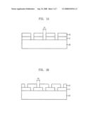
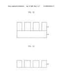
[0005]FIGS. 1A to 1D are cross-sectional views of a method for forming fine patterns in a typical semiconductor device.
[0006]Referring to FIG. 1A, after a hard mask layer 11 is formed over an etch target layer 10, the hard mask layer 11 is coated with a first photoresist layer. The first photoresist layer is patterned by exposing and developing processes and then photoresist patterns 12 are formed. The photoresist patterns 12 have a space width S1. Next, the hard mask layer 11 is etched using the first photoresist patterns 12 as an etch mask.
[0007]Referring to FIG. 1B, after removing the first photoresist patterns 12, a second photoresist layer is deposited on the resultant structure and exposing and developing processes are applied to the second photoresist layer to form the second photoresist patterns 13. The second photoresist patterns 13 have a space width S2. The openings of the second photoresist patterns 13 are formed in such a manner that they do not overlap with the openings of the first photoresist patterns 12.
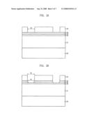
[0008]Referring to FIG. 1C, the hard mask layer 11 is etched using the second photoresist patterns 13 as an etch mask, thereby forming hard mask patterns 11'. Since the hard mask patterns 11' are formed by two etching processes, the line and space widths of the hard mask patterns 11' are reduced.
[0009]Referring to FIG. 1D, the etch target layer 10 is etched using the hard mask patterns 11' as an etch mask so that etch target patterns 10' are formed. At this time, the etch target patterns 10' have the line and space widths which are correspondent to the line and space widths of the hard mask patterns 11'.
[0010]However, even if this double patterning process is applied to the pattern formation, it is still difficult to form the micro patterns of less than 20 nm. The reason for the difficulties of the pattern formation is as follows.
[0011]In the pattern formation using the double patterning process, the most importance is to reduce the space widths (S1 and S2 in FIGS. 1A and 1B) between the first and the second photoresist patterns which are used as the etch masks. However, it is difficult to form the space widths of less than 20 nm because of the limit of the current photolithography apparatus. If the space widths between the photoresist patterns are formed in a range of below 20 nm, the failure to the device may be caused by the bridges and bad patterns. Therefore, it is very difficult to form the fine patterns of less than 20 nm through the photoresist patterns which have the space widths of less than 20 nm.
[0012]Further, in case a lower layer is etched using a general photoresist pattern, the wider the space widths formed in the lower layer is, the higher the aspect ratio of the lower layer is. Therefore, it is difficult to form the micro patterns in case the aspect ratio of the lower layer (the hard mask layer and/or the etch target layer) under the photoresist pattern is higher.
[0013]Accordingly, the technology capable of forming the fine patterns is needed in a state where the space widths of the photoresist patterns are wide and the aspect ratio of the lower layer is high.
SUMMARY OF THE INVENTION
[0014]Embodiments of the present invention are directed to providing a method for forming fine patterns in a semiconductor device by providing a positive slope for a lateral profile of a hard mask layer at the time of patterning a hard mask layer even if space widths of photoresist patterns are wide and an aspect ratio of a lower layer under the photoresist patterns is high.
[0015]In accordance with an aspect of the present invention, there is a provided a method for forming fine patterns in a semiconductor device. The method includes forming a first hard mask layer and a second hard mask layer over an etch target layer, forming second hard mask patterns by etching the second hard mask layer, wherein an etching profile of the second hard mask layer has a positive slope, and etching the first hard mask layer and the etch target layer using the second hard mask patterns as an etch mask.
BRIEF DESCRIPTION OF THE DRAWINGS
[0016]FIGS. 1A to 1D are cross-sectional views of a method for forming fine patterns in a typical semiconductor device.
[0017]FIGS. 2A to 23 are cross-sectional views of a method for forming fine patterns in accordance with an embodiment of the present invention.
DESCRIPTION OF SPECIFIC EMBODIMENTS
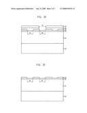
[0018]FIGS. 2A to 2J are cross-sectional views of a method for forming fine patterns in accordance with an embodiment of the present invention.
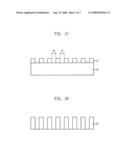
[0019]Referring to FIG. 2A, a hard mask layer, which has a stacked structure of an amorphous carbon layer 21, a silicon oxy-nitride (SiON) layer 22 and an aluminum oxide (Al2O3) layer 23, is formed. An etch target layer 20 and a first anti-reflection layer 24 are formed over the Al2O3 layer 23. At this time, etch target layer 20 can be made of a nitride layer.
[0020]Subsequently, a first photoresist layer is deposited on the first anti-reflection layer 24 and the first photoresist layer is patterned through exposing and developing processes in order to form photoresist patterns 25. Preferably, the first photoresist layer is of negative tone. In FIG. 2A, S3 denotes a space width between the photoresist patterns 25.
[0021]Referring to FIG. 2B, the first anti-reflection layer 24 is etched using the first photoresist patterns 25 as an etch mask. At this time, the etching process of the first anti-reflection layer 24 can be performed by using one selected from N2/O2, N2/H2, Cl2/O2 and CF4/O2 and a gas mixture thereof.
[0022]Next, the Al2O3 layer 23 is etched using the first photoresist patterns 25 as an etch mask. At this time, the etching process of the Al2O3 layer 23 is performed in such a manner that the Al2O3 layer 23 has a positive slope in its lateral profile. Accordingly, a space width S4 between the patterned Al2O3 layers 23 is narrower than the space width S3 between the photoresist patterns 25.
[0023]The etching process of the Al2O3 layer 23 can be performed based on a BCl3 gas. Moreover, the slope of the lateral profile of the Al2O3 layer 23 is controlled by a temperature of a wafer chuck. That is, the slope of the lateral profile is perpendicularly formed when the temperature of the wafer chuck is high and formed with a relatively large value in a positive direction when the temperature of the wafer chuck is low. Accordingly, it is possible to control the slope of the lateral profile of the Al2O3 layer 23 by controlling the temperature of the wafer chuck according to the space width S3 between the first photoresist patterns 25. Accordingly, it is possible to control the space width S4 between the patterned Al2O3 layers 23 by controlling the slope of the lateral profile of the Al2O3 layer 23.
[0024]Referring to FIG. 2C, after removing the first photoresist patterns 25 and the first anti-reflection layer 24, a post cleaning process is performed. At this time, the removal of the first photoresist patterns 25 can be performed by a removal process using O2 plasma.
[0025]Referring to FIG. 2D, a second anti-reflection layer 26 is formed over the resulting structure. A second photoresist layer is deposited on the second anti-reflection layer 26 and second photoresist patterns 27 are formed through exposing and developing processes. In the preferred embodiment of the present invention, the second photoresist layer is of negative tone. The distance between the second photoresist patterns 27 is denoted as a space width S5. Openings of the second photoresist patterns 27 are not overlapped with the openings of the Al2O3 layer 23. Preferably, the openings of the second photoresist patterns 27 are disposed to divide each pattern of the Al2O3 layer 23 into two sections.
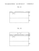
[0026]Referring to FIG. 2E, the second anti-reflection layer 26 is etched using the second photoresist patterns 27 as an etch mask. At this time, the etching process of the second anti-reflection layer 26 can be performed by using one selected from N2/O2, N2/H2, Cl2/O2 and CF4/O2 gases or a gas mixture thereof.
[0027]Subsequently, the Al2O3 layer 23 is etched again using the second photoresist patterns 27 as an etch mask. The etching condition of the Al2O3 layer 23 is identical with that described in FIG. 2B. That is, the etching process of the Al2O3 layer 23 is performed in order that the lateral profile has a positive slope. As a result, a space width S6 of the Al2O3 layer 23 is narrower than the space width S5 of the second photoresist patterns 27. Moreover, while the etching process of the Al2O3 layer 23 is carried out through a BCl3 gas, the lateral slope is controlled by the temperature of the wafer chuck. This secondary etching process is carried out by the same conditions which are applied to the first etching process in FIG. 2B.
[0028]Referring to FIG. 2F, after removing the second photoresist patterns 27 and the second anti-reflection layer 26, a post cleaning process is performed. Also, the removal of the second photoresist patterns 27 can be performed by a removal process using 02 plasma.
[0029]Consequently, Al2O3 patterns 23' are formed by these two etching processes. The Al2O3 patterns 23' have the space widths S4 and S6 which are narrower than the space widths S3 and S4 of the first and the second photoresist patterns 25 and 27. Therefore, in case that a lower layer (the SiON layer 22), the amorphous carbon layer 21 and the etch target layer 20 is etched in the subsequent processes, the fine patterns with the narrower space width are produced.
[0030]That is, since the space widths themselves between the photoresist patterns cannot be reduced by the double patterning technique used in the typical photolithography technology, the method for reducing the space widths between the hard mask patterns (especially, the Al2O3 patterns 23') is used.
[0031]However, in case this method for reducing the space widths is not sufficient for the fine patterns, an additional process can be further employed and this additional process will be described in detail referring to FIG. 2G.
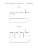
[0032]Referring to FIG. 2G, polymer layers 28 are formed on the sidewalls of the Al2O3 patterns 23' and the SiON layer 22 while the SiON layer 22 is etched using the Al2O3 patterns 23' as an etch mask. These polymer layers 28 are formed by etching the SiON layer 22 using a CF-based gas. Fluorine radical of the CF-based gas combine with the Al2O3 atoms of the Al2O3 patterns 23' and AlF3 polymer is then generated. Since the nonvolatile characteristic of the AlF3 polymer is high, the AlF3 polymer is easily deposited on the sidewalls of the Al2O3 patterns 23' and the SiON layer 22.
[0033]After forming the polymer layers 28, the space widths are much narrower than the space widths S4 and S6 between the Al2O3 patterns 23'. The generation of the AlF3 polymer can be controlled by controlling a flow rate of the CF-based gas and the ratio of fluorine (F) to carbon (C) and the space widths S7 are also controlled by such a generation of the AlF3 polymer.
[0034]Referring to FIG. 2H, the amorphous carbon layer 21 is etched using the Al2O3 patterns 23' (the Al2O3 patterns 23' and the polymer layers 28 in case the additional process in FIG. 2G is added) as an etch mask. The amorphous carbon patterns 21' are formed with the narrower space widths which are correspondent to the space widths S4 and S6 between the Al2O3 patterns 23' (or correspondent to the space widths S7 in case the additional process in FIG. 2G is added). Although the Al2O3 patterns 23' and the polymer layers 28 can be lost when the amorphous carbon layer 21 is etched, the narrower space width S7 is still available.
[0035]Referring to FIGS. 2I and 2J, after forming patterns 20' with the narrow space widths by etching the etch target layer 20 using the amorphous carbon patterns 21' as an etch mask, the amorphous carbon patterns 21' are removed. The space widths between the patterns 20' can be reduced, for example, less, than 20 nm and this reduction can be also achieved in the case that the aspect ratio of the etch target layer 20 is high.
[0036]As apparent from the above, the present invention can form the fine patterns in a semiconductor device by providing the positive slope for the lateral profile of the hard mask layer at the time of patterning the hard mask layer even if the space widths of photoresist patterns are wide and an aspect ratio of a lower layer under the photoresist patterns is high.
[0037]While the present invention has been described with respect to the particular embodiments, it will be apparent to those skilled in the art that various changes and modifications may be made without departing from the spirit and scope of the invention as defined in the following claims.
User Contributions:
comments("1"); ?> comment_form("1"); ?>Inventors list |
Agents list |
Assignees list |
List by place |
Classification tree browser |
Top 100 Inventors |
Top 100 Agents |
Top 100 Assignees |
Usenet FAQ Index |
Documents |
Other FAQs |
User Contributions:
Comment about this patent or add new information about this topic:
Images included with this patent application:
 |  |
 |  |
 |  |
 |  |
| New patent applications in this class: | |
| Date | Title |
|---|---|
| 2016-07-07 | Lithography process on high topology features |
| 2016-06-16 | Method for producing nanoimprint mold |
| 2016-06-09 | Methods of forming fine patterns and methods of manufacturing integrated circuit devices using the methods |
| 2016-05-26 | Monomer, polymer, organic layer composition, organic layer, and method of forming patterns |
| 2016-05-12 | Methods of forming features |
| New patent applications from these inventors: | |
| Date | Title |
|---|---|
| 2008-09-25 | Method for forming fine patterns in semiconductor device |
| Top Inventors for class "Etching a substrate: processes" | |
| Rank | Inventor's name |
|---|---|
| 1 | Yoshiyuki Kamata |
| 2 | Masatoshi Sakurai |
| 3 | Shou-Shan Fan |
| 4 | Yi Zheng |
| 5 | Hironori Araki |