Patent application title: TIME SEQUENCE CIRCUIT FOR POWER SUPPLY UNIT
Inventors:
Hai-Qing Zhou (Shenzhen, CN)
Hai-Qing Zhou (Shenzhen, CN)
Assignees:
HON HAI PRECISION INDUSTRY CO., LTD.
HONG FU JIN PRECISION INDUSTRY (ShenZhen) CO., LTD.
IPC8 Class: AH03L502FI
USPC Class:
327142
Class name: Signal converting, shaping, or generating synchronizing reset (e.g., initializing, starting, stopping, etc.)
Publication date: 2014-07-03
Patent application number: 20140184283
Abstract:
A time sequencing circuit for a power supply unit to ensure the correct
sequencing of system voltages for a computer from a power supply unit
includes first to ninth resistors, first to fifth electronic switches,
and a capacitor. Each of the first to fifth electronic switches includes
first to third terminals. When the power supply unit outputs all required
voltages, the power supply unit outputs a high-voltage level indicating
power good and the computer can start up. If any one of the required
voltages is not being outputted, the power supply unit outputs a
low-voltage level good signal until any non-output of voltage is cured.Claims:
1. A time sequence circuit, comprising: a first to ninth resistor; a
first to fifth electronic switch each comprising a first terminal, a
second terminal, and a third terminal; and a capacitor; wherein the first
terminal of the first electronic switch is coupled to a first power
terminal through the first resistor, connected to ground through the
second resistor, and the second terminal of the first electronic switch
is connected to ground; the first terminal of the second electronic
switch is coupled to a second system power terminal through the third
resistor, and is connected to ground through the fourth resistor, the
second terminal of the second electronic switch is coupled to the third
terminal of the first electronic switch, the first terminal of the third
electronic switch is coupled to a third system power terminal through the
fifth resistor, and is connected to ground through the sixth resistor,
the second terminal of the third electronic switch is coupled to the
third terminal of the second electronic switch, and the third terminal of
the third electronic switch is coupled to a stand-by power terminal, and
is coupled to the first terminal of the fourth electronic switch; the
second terminal of the fourth electronic switch is connected to ground,
and the third terminal of the fourth electronic switch is coupled to the
stand-by power terminal through the eighth resistor, and is connected to
ground through the capacitor; the third terminal of the fourth electronic
switch is used to output a power good signal, the first terminal of the
fifth electronic switch receives a power on signal, the second terminal
of the fifth electronic switch is connected to ground, and the third
terminal of the fifth electronic switch is coupled to the third terminal
of the fourth electronic switch; when the first terminals of the first to
fifth electronic switches are at a low-voltage level, the second and
third terminals of each electronic switch are disconnected from each
other; when the first terminals of the first to fifth electronic switches
are at a high-voltage level, the second and third terminals of each
electronic switch are connected to each other.
2. The time sequence circuit of claim 1, further comprising a tenth resistor, wherein the first terminal of the fifth electronic switch receives the power on signal through the tenth resistor.
3. The time sequence circuit of claim 2, wherein the first to fifth electronic switches are n-channel metal oxide semiconductor field effect transistors (NMOSFETs), and the first terminals, second terminals, and the third terminals of the first to fifth electronic switches are gates, sources, and drains of the NMOSFETs, respectively.
Description:
BACKGROUND
[0001] 1. Technical Field
[0002] The present disclosure relates to a time sequence circuit for a power supply unit.
[0003] 2. Description of Related Art
[0004] During a power-on operation of a computer, a motherboard of the computer may change a power-on signal PS_ON from a high-voltage level to a low-voltage level. When a power supply unit receives the low-voltage level power-on signal PS_ON, the power supply unit simultaneously outputs different voltages, such as 3V3, 5V_SYS, 5V_STBY, and 12V_SYS voltages. When all the different voltages are being outputted, the power supply unit outputs a high-voltage level power good signal after 100-500 milliseconds, and then the computer can start up. However, a user may have different types of power supply units, of which the sequencing of the power supply unit is unsuitable for the motherboard.
[0005] Therefore, there is room for improvement in the art.
BRIEF DESCRIPTION OF THE DRAWING
[0006] Many aspects of the present disclosure can be better understood with reference to the following drawing(s). The components in the drawing(s) are not necessarily drawn to scale, the emphasis instead being placed upon clearly illustrating the principles of the present disclosure.
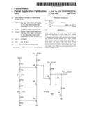
[0007] The FIGURE is a circuit diagram of an embodiment of a time sequence circuit for a power supply unit.
DETAILED DESCRIPTION
[0008] The disclosure is illustrated by way of example and not by way of limitation in the figures of the accompanying drawings in which like references indicate similar elements. It should be noted that references to "an" or "one" embodiment in this disclosure are not necessarily to the same embodiment, and such references mean "at least one."
[0009] The figure illustrates an embodiment of a time sequence circuit for a power supply unit.
[0010] The time sequence circuit comprises ten resistors R1-R10, five metal oxide semiconductor field effect transistors (MOSFETs) Q1-Q5, and a capacitor C1.
[0011] A gate of the MOSFET Q1 is coupled to a system power terminal 3.3V through the resistor R1, and is connected to ground through the resistor R2. A drain of the MOSFET Q1 is coupled to a stand-by power terminal 5V_STBY through the resistor R7, and is also coupled to a gate of the MOSFET R4. A gate of the MOSFET Q2 is coupled to a system power terminal 5V_SYS through the resistor R3, and is connected to ground through the resistor R4. A drain of the MOSFET Q2 is coupled to a source of the MOSFET Q1. A gate of the MOSFET Q3 is coupled to a system power terminal 12V_SYS through the resistor R5, and is connected to ground through the resistor R6. A source of the MOSFET Q3 is connected to ground, and a drain of the MOSFET Q3 is coupled to a source of the MOSFET Q2. A source of the MOSFET Q4 is connected to ground, and a drain of the MOSFET Q4 is coupled to the stand-by power terminal 5V_STBY through the resistor R8, and is connected to ground through the capacitor C1. The drain of the MOSFET Q4 outputs a power good signal (PWR_GOOD). A gate of the MOSFET Q5 is coupled to a motherboard through the resistor R9, to receive a power on signal PS_ON from a motherboard. A source of the MOSFET Q5 is connected to ground, and a drain of the MOSFET Q5 is coupled to the drain of the MOSFET Q4 through the resistor R10.
[0012] During a power-on operation, if one of the system power terminals 3.3V, 5V_SYS, and 12V_SYS fails to output a system voltage, one of the MOSFETs Q1, Q2, or Q3 is turned off. For example, if the system power terminal 3.3V does not output that system voltage, the MOSFETs Q2 and Q3 are turned on, and the MOSFET Q1 is turned off. The gate of the MOSFET Q4 is coupled to the system power terminal 5V_STBY through the resistor R7, and the MOSFET Q4 is turned on. Resistances of the resistors R3-R6 can be changed to make the bases of the MOSFETs Q2 and Q2 be at a high-voltage level, such as logic 1, to make the MOSFETs Q1 and Q2 turn on. The power on signal PS_ON is at a low-voltage level, such as logic 0. During the power on operation, the MOSFET D5 is turned off, and the drain of the MOSFET Q4 is at a low-voltage level. Accordingly, the MOSFET Q4 outputs a low-voltage level power good signal.
[0013] During the power-on operation, when the system power terminals 3.3V, 5V_SYS, and 12V_SYS all output system voltages, the MOSFETs Q1, Q2, and Q3 are turned on, and the gate of the MOSFET Q4 is at the low-voltage level. Accordingly, the MOSFET Q1 is turned off, and the drain of the MOSFET Q4 is at a high-voltage level. The stand-by power terminal 5V_STBY charges the capacitor C1 by way of delay for a predefined time duration. When the capacitor C1 is fully charged, the drain of the MOSFET Q4 then outputs the high-voltage level power good signal.
[0014] When in a stand-by state, the power on signal PS_ON is at the high-voltage level. Thus, the MOSFET Q5 is turned on, making the drain of the MOSFET Q4 output a low-voltage level, that is, a power good signal.
[0015] In the embodiment, the transistors Q1 and Q2 are npn-type transistors. In other embodiments, the transistors can be replaced by other electronic switches, such as metal-oxide semiconductor field-effect transistors.
[0016] While the disclosure has been described by way of example and in terms of a preferred embodiment, it is to be understood that the disclosure is not limited thereto. On the contrary, it is intended to cover various modifications and similar arrangements as would be apparent to those skilled in the art. Therefore, the range of the appended claims should be accorded the broadest interpretation so as to encompass all such modifications and similar arrangements.
User Contributions:
Comment about this patent or add new information about this topic:
| People who visited this patent also read: | |
| Patent application number | Title |
|---|---|
| 20140184196 | NANOSCALE WIRES, NANOSCALE WIRE FET DEVICES, AND NANOTUBE-ELECTRONIC HYBRID DEVICES FOR SENSING AND OTHER APPLICATIONS |
| 20140184195 | POWER QUALITY MEASURING DEVICE USED IN DISTRIBUTION LINE FOR INTEGRATED VOLTAGE AND VAR CONTROL |
| 20140184194 | MEASUREMENT APPARATUS AND ELECTRONIC DEVICE |
| 20140184193 | APPARATUS AND METHOD FOR SELECTING OPTIMUM ELECTRICAL POWER CONVERTER FOR VARIABLE POWER SOURCE |
| 20140184192 | DEVICE FOR LOCATING OBJECTS AND COLLECTING DEBRIS AND ASSOCIATED METHOD |
Images included with this patent application:
 |  |
| Similar patent applications: | |
| Date | Title |
|---|---|
| 2009-08-27 | Power supply unit |
| 2011-03-17 | Power supply unit |
| 2014-07-03 | Switch architecture at low supply voltages |
| 2014-07-10 | Phase frequency detector circuit |
| 2013-10-24 | Intelligent power supervisor |
| New patent applications in this class: | |
| Date | Title |
|---|---|
| 2017-08-17 | Clock generation circuit, interface circuit and semiconductor system using the same |
| 2016-07-14 | Apparatus and method for fast phase locking for digital phase locked loop |
| 2016-07-14 | Method for calibrating a clock signal generator in a reduced power state |
| 2016-06-30 | Output control circuit for semiconductor apparatus and output driving circuit including the same |
| 2016-06-09 | Clock conditioner circuitry with improved holdover exit transient performance |
| New patent applications from these inventors: | |
| Date | Title |
|---|---|
| 2015-07-09 | Computing device and method for automatically processing product change notice of electronic products |
| 2015-07-09 | Computing device and method for recording system event logs of computing device |
| 2015-07-02 | Power supply circuit |
| 2015-01-29 | Power supply circuit for central processing unit |
| 2015-01-29 | Power supply circuit for central processing unit |
| Top Inventors for class "Miscellaneous active electrical nonlinear devices, circuits, and systems" | |
| Rank | Inventor's name |
|---|---|
| 1 | Yantao Ma |
| 2 | Feng Lin |
| 3 | Ming-Chieh Huang |
| 4 | Yong-Ju Kim |
| 5 | Chan-Hong Chern |