Patent application title: METHOD FOR FORMING TIN BY PVD
Inventors:
Zuozhen Fu (Beijing, CN)
Huaxiang Yin (Beijing, CN)
Huaxiang Yin (Beijing, CN)
Jiang Yan (Beijing, CN)
IPC8 Class: AH01L2102FI
USPC Class:
438785
Class name: Coating of substrate containing semiconductor region or of semiconductor substrate insulative material deposited upon semiconductive substrate insulative material is compound of refractory group metal (i.e., titanium (ti), zirconium (zr), hafnium (hf), vanadium (v), niobium (nb), tantalum (ta), chromium (cr), molybdenum (mo), tungsten (w), or alloy thereof)
Publication date: 2014-01-16
Patent application number: 20140017906
Abstract:
A method for forming titanium nitride by PVD is disclosed, comprising:
generating ions of a noble gas by glow discharge under a vacuum condition
that a nitrogen gas and the noble gas are supplied; nitriding a surface
of a wafer and a surface of a titanium target with the nitrogen gas;
bombarding the surface of the titanium target with the ions of the noble
gas after they are accelerated in an electric field so that titanium ions
and titanium nitride are sputtered; and forming a titanium nitride layer
by depositing titanium nitride on the surface of the wafer in a magnetic
field, while titanium ions are injected into the surface of the wafer so
that stress is introduced into the titanium nitride layer, wherein
non-crystallization fraction of the titanium nitride layer and stress in
the titanium nitride layer are increased by increasing kinetic energy of
titanium ions which are injected into the surface of the wafer. In the
method for forming titanium nitride by PVD according to the present
disclosure, kinetic energy of titanium ions which are injected into the
surface of the wafer is increased by controlling process parameters so
that non-crystallization fraction of the titanium nitride layer and
stress in the titanium nitride layer are increased.Claims:
1. A method for forming titanium nitride by PVD, comprising: generating
ions of a noble gas by glow discharge under a vacuum condition that a
nitrogen gas and the noble gas are supplied; nitriding a surface of a
wafer and a surface of a titanium target with the nitrogen gas;
bombarding the surface of the titanium target with the ions of the noble
gas after they are accelerated in an electric field so that titanium ions
and titanium nitride are sputtered; and forming a titanium nitride layer
by depositing titanium nitride on the surface of the wafer in a magnetic
field while titanium ions are injected into the surface of the wafer so
that stress is introduced into the titanium nitride layer, wherein
non-crystallization fraction of the titanium nitride layer and stress in
the titanium nitride layer are increased by increasing kinetic energy of
titanium ions which are injected into the surface of the wafer.
2. The method according to claim 1, wherein increasing kinetic energy of titanium ions which are injected into the surface of the wafer comprises: decreasing a distance between the wafer and the titanium target.
3. The method according to claim 2, wherein the distance between the wafer and the titanium target is about 190 mm to 260 mm.
4. The method according to claim 1, wherein increasing kinetic energy of titanium ions which are injected into the surface of the wafer comprises: increasing sputtering power.
5. The method according to claim 4, wherein the sputtering power is about 100 w to 2000 w.
6. The method according to claim 1, further comprising increasing a flow rate of nitrogen gas.
7. The method according to claim 6, wherein the flow rate of nitrogen gas is about 1.5 to 10.0 SCCM.
8. The method according to claim 1, further comprising decreasing a thickness of the titanium nitride layer.
9. The method according to claim 8, wherein the thickness of the titanium nitride layer is about 6 to 100 nm.
10. The method according to claim 1, wherein the stress in the titanium nitride layer is about 0 to -6.5 GPa.
Description:
CROSS-REFERENCE TO RELATED APPLICATION
[0001] This application claims priority to the Chinese Patent Application No. 201210245146.3, filed on Jul. 13, 2012, entitled "Method for Forming TiN by PVD", which is incorporated herein by reference in its entirety.
TECHNICAL FIELD
[0002] The present disclosure relates to a method form manufacturing a semiconductor device, and particularly to a method for forming a TiN film by PVD.
BACKGROUND
[0003] With continuous development of large-scale integrated circuits, an integration level of integrated circuits is continuously increased and a feature size of MOSFETs is decreased beyond the 22 nm node. Actually, it becomes more and more difficult to fulfill the requirement of Moor law after the 90 nm node by simply reducing a gate length. When the gate length is reduced, heavily doping is performed in a channel region for suppressing short channel effects, which, however, causes scattering due to the channel doping and a strong field effect and increased parasitic resistance. Consequently, mobility of carriers in the channel region is decreased, which impairs improvement of electrical performances of the device. In view of this, stress engineering is proposed as a important approach to increasing mobility of carriers in the channel region.
[0004] Such an approach utilizes various sources of stress to apply stress to the channel region in the manufacture of the device, such as strained overlayers, stress memorization, and embedded SiGe (eSiGe). The stress, if being appropriately applied, will increase mobility of carriers in the channel region and improve electrical performances of the device even in a case that a size of the channel region is continuously reduced.
[0005] A metal gate is widely used in a CMOS device after the 45 nm node. As an extension of SMT technique, an approach of introducing the stress to the channel region by the metal gate is proposed as required, especially for an NMOS device. Thus, it is a necessary task to study the NMOS device with TiNx as a material of the metal gate and to study its stress effect.
[0006] Conventional methods for forming a TiN film, such as evaporation, (magnetron) sputtering, PECVD, etc., may obtain a TiNx film with 1 to 2 GPa stress by controlling process parameters. However, with continuous reduction of the device size, a demand on increasing carrier mobility in the channel region is increased. It is difficult for the conventional methods for forming the TiNx film as described above to fulfill the requirement for increasing driving capability of the device by varying process parameters.
SUMMARY OF THE DISCLOSURE
[0007] One object of the present disclosure is to increase stress by optimizing process parameters of a method for forming a TiN film by PVD so as to increase mobility of carriers in a channel region and in turn to improve performances of the device.
[0008] To this end, there is provided a method for forming titanium nitride by PVD is disclosed, comprising: generating ions of a noble gas by glow discharge under a vacuum condition that a nitrogen gas and the noble gas are supplied; nitriding a surface of a wafer and a surface of a titanium target with the nitrogen gas; bombarding the surface of the titanium target with the ions of the noble gas after they are accelerated in an electric field so that titanium ions and titanium nitride are sputtered; and forming a titanium nitride layer by depositing titanium nitride on the surface of the wafer in a magnetic field, while titanium ions are injected into the surface of the wafer so that stress is introduced into the titanium nitride layer, wherein non-crystallization fraction of the titanium nitride layer and stress in the titanium nitride layer are increased by increasing kinetic energy of titanium ions which are injected into the surface of the wafer.
[0009] Preferably, increasing kinetic energy of titanium ions which are injected into the surface of the wafer may comprise: reducing a distance between the wafer and the titanium target. Preferably, a distance between the wafer the titanium target may be about 190 mm-260 mm.
[0010] Preferably, increasing kinetic energy of titanium ions which are injected into the surface of the wafer may comprises: increasing sputtering power. Preferably, the sputtering power may be about 100 w to 2000 w.
[0011] Preferably, a flow rate of nitrogen gas may also be increased. Preferably, the flow rate of the nitrogen gaps may be about 1.5 to 10.0 SCCM.
[0012] Preferably, a thickness of the titanium nitride layer may also be decreased. Preferably, the thickness of the titanium nitride layer may be about 6 to 100 nm.
[0013] Preferably, stress in the titanium nitride layer may be about 0 to -6.5 GPa.
[0014] In the method for forming titanium nitride by PVD according to the present disclosure, kinetic energy of titanium ions which are injected into the surface of the wafer is increased by controlling process parameters so that non-crystallization fraction of the titanium nitride layer and stress in the titanium nitride layer are increased.
BRIEF DESCRIPTION OF THE DRAWINGS
[0015] The solutions according to the present disclosure will be described in detail with reference to the drawings, in which:
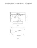
[0016] FIG. 1 schematically shows a method for depositing a TiN film by sputtering in an embodiment according to the present disclosure; and
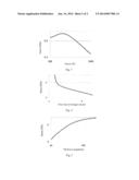
[0017] FIGS. 2 to 5 are graphs showing stress in the TiNx film versus a distance between a target and a wafer, power, a flow rate, and a thickness, respectively.
DETAILED DESCRIPTION
[0018] Technical features and effects of the solutions of the present disclosure, which are directed to methods for forming TiNx by PVD, will be described below in detail with reference to attached drawings. It should be noted that similar reference numbers denote similar structures. The words "first", "second", "upper", and "lower" may be used in the present application for describing various structures of the device and various steps of the process. However, these words do not imply any spatial, sequential or hierarchy relation of various structures of the device and various steps of the process, unless the context clearly indicates otherwise.
[0019] The present disclosure may be implemented by forming TiNx in conventional (magnetron) sputtering apparatus It should be noted that titanium nitride is sometimes referred to as "TIN" for simplicity in the context of the present application. That is, the content x of N is omitted. However, it does not mean that the content x should be exactly the integer "1". Actually, the content x may be any number from 0 to 4 and may not be limited to an integer.
[0020] As shown in FIG. 1, ions of a noble gas (He, Ne, Ar, Kr, Xe etc., preferably Ar, and atoms with larger atomic weight to improve bombarding and sputtering effects) are generated during ionization by glow discharge of the noble gas under a vacuum condition that a reactive gas (i.e. nitrogen gas) and a sputtering gas (i.e. the noble gas) are supplied. For example, chamber pressure during sputtering is maintained at about 8 mtorr. Meanwhile, a surface of the Ti target and a surface of a wafer (for example, a monocrystalline Si wafer) are nitrided by nitrogen gas. The ions of the noble gas are accelerated in an electric field and bombard the surface of the Ti target to sputter atoms of TIN. Due to the electric field, the atoms of TIN reach the wafer and are deposited as a TiN film. In the above process, the noble gas such as Ar or the like, in addition to the atoms of TiN that reach the wafer, will also bombard the surface of the Ti target to sputter Ti ions. The Ti ions on one hand react with the nitrogen gas, and one the other hand continuously bombard the TIN film which has already been formed on the wafer so that the TiN film on the surface of the wafer is locally non-crystallized and is thus introduced with stress.
[0021] The inventor proposes a key solution of the present disclosure on the basis of theoretical analysis and many times of experiments for verifying the theoretical analysis. The key solution is that non-crystallization fraction of the TiN and stress in the TIN may be increased by increasing kinetic energy of Ti ions which are injected into the surface of the wafer.
[0022] Specifically, the kinetic energy of Ti ions which are injected into the surface of the wafer may be increased by:
[0023] 1) shortening a distance D between the wafer and the target holder in FIG. 1. In a conventional sputtering chamber, the distance D is typically 260 mm. As a comparison, the distance is decreased to about 190 mm in an embodiment according to the present disclosure. Due to a shorter distance, an electric filed is enhanced even at the same voltage. As a result, the Ti ions are accelerated more in the electric field so that the non-crystallization fraction of the TiN film on the surface of the wafer is remarkably increased, which in turn effectively increases the stress in the TiN film, It is apparent from FIG. 2 that the stress in the TiN film is remarkably increased with a shorter distance in the range of 190 mm to 260 mm. Thus, the distance D should be shortened as much as possible.
[0024] 2) increasing sputtering power. In a conventional sputtering chamber, the sputtering power is typically 50 to 200 w. As a comparison, the sputtering power is increased in the method according to the present disclosure. For example, the sputtering power is in the range of about 100 w to 2000 w, and preferably in the range of about 800 w to 2000 w, and more preferably in the range of about 1500 w to 2000 w. It is apparent from FIG. 3 that the electromagnetic field is enhanced even at the same distance when the sputtering power is increased in the range of about 100 w to 2000 w, and the TiN ions have larger kinetic energy. As a result, the non-crystallization fraction of TIN is increased, which in turn increases the stress in the film. Thus, the sputtering power should be increased as much as possible.
[0025] Moreover, the stress in the film may be increased by increasing a flow rate of nitrogen gas in the method according to the present disclosure. It is apparent from FIG. 4 that the stress in the film is increased with an increased flow rate of nitrogen gas. This is because a larger content of N in TiN varies crystal lattice of the film, which in turn increases intrinsic stress. Preferably, the flow rate of nitrogen gas in the present disclosure may be about 1.5 to 10.0 SCCM, more preferably about 3.0 to 10.0 SCCM, and most preferably about 7.5 to 10.0 SCCM.
[0026] It is apparent from FIG. 5 that stress in TIN is remarkably increased when a thickness of the resultant TiN film on the wafer is decreased. This is because fine cracks in crystal lattice of the TIN film with a small thickness propagate into a larger relative depth with respect to the thickness of the TIN film, even in a case that kinetic energy of Ti ions is the same. That is, the non-crystallization fraction of TiN film due to bombardment of Ti ions is increased, which in turn increases the local stress in the filmln an embodiment according to the present disclosure, the thickness of the TIN film may be 6 to 100 nm. preferably 6 to 50 nm, and more preferably 6 to 10 nm.
[0027] In summary, as shown in FIGS. 2 to 5, the stress of the resultant TIN film may be as large as -6.5 GPa, for example in the range of +1.0 to -6.5 Gpa, and preferably in the range of 0 to -6.5 GPa, by optimizing various process parameters. The stress is much larger than the stress (±2 GPa at most) achieved in conventional PECVD magnetron sputtering processes.
[0028] In the method for forming titanium nitride by PVD according to the present disclosure, kinetic energy of titanium ions which are injected into the surface of the wafer is increased by controlling process parameters so that non-crystallization fraction of the titanium nitride layer and stress in the titanium nitride layer are increased.
[0029] The present disclosure has been described above with reference to one or more embodiments thereof. It should be understood that various modifications, alternations and additions can be made to the device structure by one skilled person in the art without departing from the spirits and scope of the present disclosure. Moreover, the teachings of the present disclosure may make various modifications which may be adapted for particular situations or materials without departing from the spirits and scope of the present disclosure. Therefore, the object of the present disclosure is not limited to the above particular embodiments as preferably implementations of the present disclosure. The device structure and the manufacture method thereof as disclosed will include all of embodiments falling within the scope of the present disclosure.
User Contributions:
Comment about this patent or add new information about this topic:
Images included with this patent application:
 |  |
 |
| Similar patent applications: | |
| Date | Title |
|---|---|
| 2011-08-18 | Method for forming polarization reversal |
| 2012-03-15 | Copper bonding compatible bond pad structure and method |
| New patent applications in this class: | |
| Date | Title |
|---|---|
| 2019-05-16 | Dry and wet etch resistance for atomic layer deposited tio2 for sit spacer application |
| 2019-05-16 | Process for the generation of metallic films |
| 2016-06-23 | Semiconductor device manufacturing method |
| 2016-03-17 | Systems and methods for reducing backside deposition and mitigatingthickness changes at substrate edges |
| 2016-03-03 | Radical-enhanced atomic layer deposition using cf4 to enhance oxygen radical generation |
| New patent applications from these inventors: | |
| Date | Title |
|---|---|
| 2021-12-09 | Semiconductor device and method for manufacturing the same |
| 2016-03-24 | Semiconductor device and method for manufacturing the same |
| 2016-03-24 | Semiconductor devices and methods for manufacturing the same |
| 2016-03-24 | Cmos device and method for manufacturing the same |
| 2016-03-10 | Method for manufacturing semiconductor device |
| Top Inventors for class "Semiconductor device manufacturing: process" | |
| Rank | Inventor's name |
|---|---|
| 1 | Shunpei Yamazaki |
| 2 | Shunpei Yamazaki |
| 3 | Kangguo Cheng |
| 4 | Chen-Hua Yu |
| 5 | Devendra K. Sadana |