Patent application title: WAFER PROCESSING METHOD
Inventors:
Kazuma Sekiya (Tokyo, JP)
Kazuma Sekiya (Tokyo, JP)
IPC8 Class: AB24B906FI
USPC Class:
451 44
Class name: Abrading process glass or stone abrading edging
Publication date: 2013-12-26
Patent application number: 20130344775
Abstract:
A wafer processing method of processing a wafer having an epitaxial film
formed on the front side. The wafer processing method includes a holding
step of holding the wafer on a holding table having a holding surface for
holding the wafer and a rotational axis extending perpendicularly to the
holding surface and passing through the center of the holding surface,
and a removing step of pressing a grinding member on a ridge portion
formed along the peripheral edge of the wafer held on the holding table
and rotating the holding table about the rotational axis, thereby
removing the ridge portion.Claims:
1. A wafer processing method of processing a wafer having an epitaxial
film formed on a front side, said wafer processing method comprising: a
holding step of holding said wafer on a holding table having a holding
surface for holding said wafer and a rotational axis extending
perpendicularly to said holding surface and passing through the center of
said holding surface; and a removing step of pressing a grinding member
on a ridge portion formed along the peripheral edge of said wafer held on
said holding table and rotating said holding table about said rotational
axis, thereby removing said ridge portion.
2. The wafer processing method according to claim 1, wherein said wafer is held on said holding table in the condition where the center of said wafer is deviated from said rotational axis of said holding table in said holding step.
3. The wafer processing method according to claim 1, wherein said wafer is formed of silicon carbide.
Description:
BACKGROUND OF THE INVENTION
[0001] 1. Field of the Invention
[0002] The present invention relates to a wafer processing method of processing a wafer having an epitaxial film formed on the front side.
[0003] 2. Description of the Related Art
[0004] Epitaxial growth on the front side of a semiconductor crystal substrate (wafer) of silicon (Si) or the like causes undesirable formation of a ridge portion of an epitaxial film, called edge crown, along the peripheral edge of the wafer. To cope with this problem, the peripheral edge of the wafer is generally formed with a chamfered portion to suppress the occurrence of abnormal growth in the epitaxial growth, i.e., the formation of the edge crown and to also prevent the occurrence of cracking or chipping due to the contact of the peripheral edge of the wafer in handling or transporting the wafer.
[0005] However, when the epitaxial film has a large thickness, the height of the edge crown is increased to more than 10 μm in some cases. In such a wafer, the formation of the edge crown cannot be suppressed by a conventional arcuate chamfered portion. To cope with this problem, Japanese Patent Laid-open No. Hei 7-226349 discloses a technique of forming a tapering chamfered portion along the peripheral edge of the wafer to suppress the height of the edge crown.
SUMMARY OF THE INVENTION
[0006] In the case that such a sufficiently large chamfered portion is formed along the peripheral edge of the wafer as mentioned above, the height of the edge crown formed during the epitaxial growth can be suppressed. However, there is a case that the chamfered portion is small or no chamfering is performed depending on the kind of the wafer. In such a wafer, an edge crown (ridge portion of the epitaxial film) is undesirably formed along the peripheral edge of the wafer during the epitaxial growth. There is a possibility that the edge crown (ridge portion of the epitaxial film) formed on the front side of the wafer along the peripheral edge thereof may be broken during transportation of the wafer to cause damage to the devices formed on the front side of the wafer. Further, when an edge crown is formed on the back side of the wafer, there is a possibility that faulty suction holding of the wafer may occur in holding the back side of the wafer under suction in a subsequent step.
[0007] An SiC semiconductor that has recently received attention has excellent physical and chemical properties and it is therefore expected that a smaller-size and lower-loss semiconductor device over a silicon (Si) semiconductor can be realized. Such an SiC semiconductor is expected to be applied to power-conversion switching devices used in various fields such as electric power, automobile, railroad, and home electrical appliance and also applied to high-performance and large-power radio-frequency devices for communications. However, there is a case that no chamfering is performed on an SiC wafer. When an epitaxial film is formed on the SiC wafer by epitaxial growth, edge crowns are formed on the front side and back side of the wafer along the peripheral edge thereof, causing the damage to the devices formed on the front side of the wafer or the faulty suction holding of the wafer in the subsequent step.
[0008] It is therefore an object of the present invention to provide a wafer processing method which can prevent the damage to the devices and the faulty suction holding of the wafer in the subsequent step due to the ridge portion of the epitaxial film, regardless of the kind of the wafer.
[0009] In accordance with an aspect of the present invention, there is provided a wafer processing method of processing a wafer having an epitaxial film formed on the front side, the wafer processing method including a holding step of holding the wafer on a holding table having a holding surface for holding the wafer and a rotational axis extending perpendicularly to the holding surface and passing through the center of the holding surface; and a removing step of pressing a grinding member on a ridge portion formed along the peripheral edge of the wafer held on the holding table and rotating the holding table about the rotational axis, thereby removing the ridge portion.
[0010] Preferably, the wafer is held on the holding table in the condition where the center of the wafer is deviated from the rotational axis of the holding table in the holding step. Preferably, the wafer is formed of silicon carbide.
[0011] According to the present invention, the ridge portion (edge crown) formed along the peripheral edge of the wafer having the epitaxial film formed on the front side is removed by grinding. Accordingly, it is possible to prevent the damage to the devices and the faulty suction holding of the wafer in the subsequent step due to the ridge portion of the epitaxial film.
[0012] The above and other objects, features and advantages of the present invention and the manner of realizing them will become more apparent, and the invention itself will best be understood from a study of the following description and appended claims with reference to the attached drawings showing some preferred embodiments of the invention.
BRIEF DESCRIPTION OF THE DRAWINGS
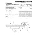
[0013] FIG. 1 is a sectional view of an SiC wafer having an epitaxial film on the front side;
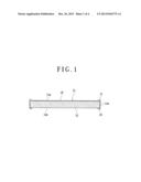
[0014] FIG. 2 is a partially sectional side view showing a holding step;
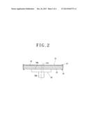
[0015] FIG. 3 is a partially sectional side view showing a removing step; and
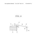
[0016] FIG. 4 is a partially sectional side view showing another preferred embodiment of the removing step.
DETAILED DESCRIPTION OF THE PREFERRED EMBODIMENTS
[0017] A preferred embodiment of the present invention will now be described in detail with reference to the drawings. Referring to FIG. 1, there is shown an SiC (silicon carbide) wafer 11. The SiC wafer 11 is composed of an SiC bulk wafer (SiC substrate) 13 and an epitaxial film 15 formed on the SiC bulk wafer 13 by epitaxial growth. That is, the epitaxial film 15 is formed as a single-crystal SiC thin film. Usually, the epitaxial film 15 of the SiC wafer 11 is formed by CVD (Chemical Vapor Deposition) or the like. The SiC wafer 11 has a front side 11a (upper surface), a back side 11b (lower surface), and a peripheral surface 11e substantially perpendicular to both the front side 11a and the back side 11b. That is, the peripheral surface 11e of the SiC wafer 11 is not formed with a chamfered portion.
[0018] In the case that the epitaxial film 15 is formed by epitaxial growth on such a wafer having no chamfered portion, e.g., the SiC wafer 11 as mentioned above, edge crowns (ridge portions) 17 and 19 are formed on the front side 11a and the back side 11b near the peripheral surface 11e. The wafer processing method of the present invention is a method of removing the edge crowns 17 and 19 from such a wafer having the edge crowns 17 and 19. As shown in FIG. 2, a holding step is first performed in such a manner that the SiC wafer 11 is held under suction on a holding table 10 having a holding surface 10a and a rotational axis 10b. The rotational axis 10b extends perpendicularly to the holding surface 10a and passes through the center of the holding surface 10a. Although not especially shown, the holding surface 10a is selectively connected to a vacuum source (not shown).
[0019] In this holding step, the SiC wafer 11 is held under suction on the holding surface 10a of the holding table 10 in the condition where the center 11c of the SiC wafer 11 does not coincide with the rotational axis 10b of the holding table 10, that is, in the condition where the center 11c of the SiC wafer 11 is deviated from the rotational axis 10b of the holding table 10. Thereafter, a removing step is performed as shown in FIG. 3 in the following manner. In this removing step, a grinding member 20 of a grinding jig 16 is pressed on the edge crown 17 of the SiC wafer 11 held on the holding table 10. The grinding jig 16 is composed of a base 18 and the grinding member 20 fixed to the lower surface of the base 18. The grinding member 20 is provided by a grinding wheel, for example. However, the grinding member 20 is not limited to a grinding wheel, but abrasive grains dispersed in a nonwoven fabric or polyurethane foam may be used, for example. Further, the term of "grinding" used in this description is regarded as also including polishing.
[0020] The grinding jig 16 is mounted through a coil spring 14 to the front end portion of an L-shaped support member 12. Accordingly, the grinding member 20 is pressed on the edge crown 17 by the biasing force of the coil spring 14. In the condition where the grinding member 20 is pressed on the edge crown 17 by the biasing force of the coil spring 14, the holding table 10 is rotated in the direction shown by an arrow a at 300 rpm, for example, so that the edge crown 17 is ground to be removed by the grinding member 20.
[0021] The SiC wafer 11 is eccentrically held on the holding table 10, so that when the holding table 10 is rotated, the edge crown 17 is oscillated in the radial direction of the wafer 11. Accordingly, the edge crown 17 is ground by the grinding member 20 as moving both in the circumferential direction of the wafer 11 and in the radial direction of the wafer 11. As a result, the grinding of the edge crown 17 is performed effectively. Further, if the SiC wafer 11 is concentrically held on the holding table 10, a part of the grinding member 20 always abuts against the edge crown 17 in the grinding operation, causing local wearing of the grinding member 20. However, since the SiC wafer 11 is eccentrically held on the holding table 10 in this preferred embodiment, such local wearing of the grinding member 20 can be prevented.
[0022] After removing the edge crown 17 formed on the front side 11a of the SiC wafer 11, a protective tape (not shown) is attached to the front side 11a of the wafer 11. In this condition, the wafer 11 is held under suction through the protective tape on the holding table 10, and the grinding member 20 is pressed on the edge crown 19 formed on the back side 11b of the SiC wafer 11 to grind the edge crown 19, thereby removing the edge crown 19.
[0023] Referring next to FIG. 4, there is shown a partially sectional side view illustrating another preferred embodiment of the removing step. In this preferred embodiment, a support member 22 for supporting the grinding jig 16 is used. The support member 22 is composed of a first arm 24 and a second arm 26 pivotably connected through a joint 28 to the front end of the first arm 24. The grinding jig 16 is mounted to the front end of the second arm 26. With this configuration, the grinding surface (lower surface) of the grinding member 20 can be inclined at a predetermined angle with respect to the epitaxial film 15 formed on the front side of the SiC bulk wafer 13 in grinding the edge crown 17. Accordingly, it is possible to prevent a problem such that the epitaxial film 15 formed on the front side of the bulk wafer 13 may be damaged by the grinding member 20 in grinding the edge crown 17. In this preferred embodiment, the joint 28 is preferably provided with a spring for biasing the second arm 26 in a counterclockwise direction as viewed in FIG. 4, thereby pressing the grinding member 20 on the edge crown 17.
[0024] While the wafer processing method of the present invention is applied to the SiC wafer 11 having no chamfered portion along the peripheral edge in each preferred embodiment mentioned above, the workpiece to be processed by the present invention is not limited to the SiC wafer 11, but the present invention is also applicable to any other wafers having no chamfered portion along the peripheral edge.
[0025] The present invention is not limited to the details of the above described preferred embodiments. The scope of the invention is defined by the appended claims and all changes and modifications as fall within the equivalence of the scope of the claims are therefore to be embraced by the invention.
User Contributions:
Comment about this patent or add new information about this topic:
| People who visited this patent also read: | |
| Patent application number | Title |
|---|---|
| 20210054782 | POWER SYSTEM FOR ROTARY WING AIRCRAFT |
| 20210054781 | POWER GENERATION DEVICE AND AUTOMOBILE |
| 20210054780 | INTERNAL-COMBUSTION ENGINE AND DRIVE SYSTEM |
| 20210054779 | WASTEGATE FOR TURBINE |
| 20210054778 | AIR INTAKE AND EXHAUST SYSTEMS FOR A SNOWMOBILE ENGINE |
Images included with this patent application:
 |  |
 |  |
 |
| Similar patent applications: | |
| Date | Title |
|---|---|
| 2013-08-22 | Wafer processing equipment |
| 2009-07-02 | Wafer production method |
| 2010-04-29 | Spectacle lens edging method |
| 2014-01-30 | Linear pressure feed grinding with voice coil |
| 2010-09-02 | Electron-beam-assisted eem method |
| New patent applications in this class: | |
| Date | Title |
|---|---|
| 2017-08-17 | High molecular weight pag coolant for grinding glass |
| 2016-01-07 | Method for manufacturing a circular wafer by polishing the periphery, including a notch or orientation flat, of a wafer comprising crystal material, by use of polishing tape |
| 2015-10-22 | Polishing apparatus and polishing method |
| 2014-11-13 | Linear pressure feed grinding with voice coil |
| 2014-10-02 | Method for polishing edge of glass substrate of display panel |
| New patent applications from these inventors: | |
| Date | Title |
|---|---|
| 2022-09-15 | Method of manufacturing wafer and method of manufacturing stacked device chip |
| 2021-11-25 | Dressing member |
| 2021-11-04 | Management method of machining system |
| 2021-10-28 | Wet etching method and wet etching system |
| 2021-10-14 | Cutting apparatus, tray, and transport system |
| Top Inventors for class "Abrading" | |
| Rank | Inventor's name |
|---|---|
| 1 | Boguslaw A. Swedek |
| 2 | Hung Chih Chen |
| 3 | Jeffrey Drue David |
| 4 | Dominic J. Benvegnu |
| 5 | Chien-Min Sung |