Patent application title: ELECTICAL CONNECTOR ASSEMBLY HAVING A BLOCK FOR STOPING A CHIP MODULE COMING OFF
Inventors:
Chun-Yi Chang (New Taipei, TW)
Chun-Yi Chang (New Taipei, TW)
IPC8 Class: AH01R1342FI
USPC Class:
439 68
Class name: Preformed panel circuit arrangement, e.g., pcb, icm, dip, chip, wafer, etc. with provision to conduct electricity from panel circuit to another panel circuit micro panel circuit arrangement, e.g., icm, dip, chip, wafer, etc.
Publication date: 2013-12-26
Patent application number: 20130344715
Abstract:
An electrical connector electrically connecting a chip module to a
printed circuit board, and includes an insulative housing, a plurality of
terminals received in the insulative housing and a block assembled to the
insulative housing, the electrical connector comprises a bottom wall and
a plurality of side walls, between the bottom wall and the side walls
forms a receiving space to receive the chip module for assembling the
chip module from top to bottom in vertical direction, the block is
configured with frame shape and comprises a plurality of tabs, the
insulative housing comprises a plurality of slots matched with the tabs,
the block can prevent the chip module coming off from the insulative
housing while the chip module received in the receiving space.Claims:
1. An electrical connector electrically connecting a chip module to a
printed circuit board, and comprising: an insulative housing comprising a
bottom wall and a plurality of side walls, between the bottom wall and
the side walls forms a receiving space to receive the chip module for
assembling the chip module from top to bottom in a vertical direction; a
plurality of terminals received in the insulative housing; and wherein
the electrical connector further comprises a block assembled to the
insulative housing, the block is configured with frame shape and
comprises a plurality of tabs, the insulative housing comprises a
plurality of slots interfered with the tabs of the block, the block can
prevent the chip module coming off from the insulative housing while the
chip module received in the receiving space.
2. The electrical connector as claimed in claim 1, wherein said block comprises a base and a plurality of extending portions, the tab protruding from the extending portion to the insulative housing.
3. The electrical connector as claimed in claim 1, wherein said slots located at the side walls of the insulative housing, each of the pair of side walls has a breach convenient to get off the chip module respectively.
4. The electrical connector as claimed in claim 1, wherein said height of the block that assembled to the insulative housing is equal to a height of the side wall, said middle of the block has an open for receiving the chip module.
5. The electrical connector as claimed in claim 1, wherein said bottom wall has a plurality of receiving holes, the electrical connector further comprises a plurality of terminals received in the receiving holes.
6. An electrical connector assembly comprising: an electrical connector, assembled to the printed circuit board, and comprising an insulative housing and a plurality of terminals received therein; a chip module assembled at the electrical connector; a block assembled at the insulative housing and pressed on the chip module; and wherein a fixing device, fixing the electrical connector to the printed circuit board, and comprising a pressing element used for pressing the chip module, the pressing element is configured with X-shape.
7. The electrical connector assembly as claimed in claim 6, wherein the block comprises a plurality of tabs, the insulative housing comprises a plurality of slots interfered with the tabs.
8. The electrical connector assembly as claimed in claim 7, wherein said block comprises a base and a plurality of extending portions, the tab protruding from the extending portion to the insulative housing, the extending portions located near the corners of the insulative housing, the slots located at the side walls of the insulative housing.
9. The electrical connector assembly as claimed in claim 6, wherein each of a pair of side walls has a breach convenient to get off the chip module respectively, the middle of the block has an open configured with frame shape.
10. The electrical connector assembly as claimed in claim 6, wherein said insulative housing comprises a bottom wall and a plurality of side walls extending upwardly from the bottom wall, the bottom wall comprises a plurality of receiving holes that the terminals received therein.
11. The electrical connector assembly as claimed in claim 6, wherein said chip module comprises a substrate and a die protruding from the substrate, the height of the block is smaller than the height of the die.
12. The electrical connector assembly as claimed in claim 9, wherein said fixing device further comprises a plurality of screws used for connecting the pressing element and to the printed circuit board, the printed circuit board has a plurality of retention portions matched with the screws.
13. The electrical connector assembly as claimed in claim 12, wherein said pressing element comprises a flat body portion and a plurality of connecting portions extending outwardly from the corners of the body portion,
14. The electrical connector assembly as claimed in claim 13, wherein each of the ends of the connecting portions have a through hole for passing through the connecting portions.
15. The electrical connector assembly as claimed in claim 12, wherein said screws passing through the pressing element and fixing the chip module to the printed circuit board along with the electrical connector to achieve the electrically connecting of the chip module and the printed circuit board.
16. An electrical connector assembly comprising: a printed circuit board; an insulative housing positioned upon the printed circuit board and including a bottom wall and a plurality of side walls extending upwardly from a peripheral region of the bottom wall to commonly define an upward facing rectangular receiving cavity; a rectangular electronic package received within the receiving cavity, said electronic package being equipped with a die raising upward at a center region of the electronic package; a retaining device located around the side walls to retain a peripheral region of the electronic package while exposing the die; and a pressing element defining a center body portion downwardly abutting against the die and plurality of connecting portions outwardly extending from the center body portion to be secured to the printed circuit board beside the housing.
17. The electrical connector assembly as claimed in claim 16, wherein said pressing element cooperates with the retaining device without interference therebetween.
18. The electrical connector assembly as claimed in claim 16, wherein the connecting portions are secured to the printed circuit board via upward retention portions and screws, respectively.
19. The electrical connector assembly as claimed in claim 16, wherein said retaining device is fully located below the body portion.
20. The electrical connector assembly as claimed in claim 16, wherein said retaining device is discrete from the housing while being securely assembled to top faces of said side walls.
Description:
BACKGROUND OF THE INVENTION
[0001] 1. Field of the Invention
[0002] The present invention relates to an electrical connector assembly, and more particularly to an electrical connector assembly fixing the chip module to the printed circuit board.
[0003] 2. Description of the Prior Art
[0004] An electrical connector assembly includes an electrical connector, the electrical connector electrically connecting a chip module to a printed circuit board is described in Tai Wan Patent No. 411,042, issued to LIAO on Sep. 1, 2011. The electrical connector includes a socket body with a plurality of electrical contacts secured therein. The chip module is pressed by the heat sink and the heat sink is fixed to the printed circuit board by a number of screws for providing the pressure of the chip module. After the chip module is assembled to the electrical connector and not fixed to the printed circuit board, the chip module may come off from it and damage the terminal. When the heat sink is locked to the printed circuit board, the chip module can not be fixed to the printed circuit board in accurate position.
[0005] Therefore, it is needed to find a new electrical socket to overcome the problems mentioned above.
SUMMARY OF THE INVENTION
[0006] Accordingly, an object of the present invention is to prevent the chip module coming off from the insulative housing.
[0007] In order to achieve the object set forth, an electrical connector electrically connecting a chip module to a printed circuit board, and comprises an insulative housing, a plurality of terminals received in the insulative housing and a block assembled to the insulative housing, the electrical connector comprises a bottom wall and a plurality of side walls, between the bottom wall and the side walls forms a receiving space to receive the chip module for assembling the chip module from top to bottom in vertical direction, the block is configured with frame shape and comprises a plurality of tabs, the insulative housing comprises a plurality of slots matched with the tabs, the block can prevent the chip module coming off from the insulative housing while the chip module received in the receiving space.
BRIEF DESCRIPTION OF THE DRAWINGS
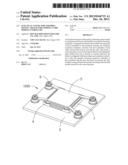
[0008] FIG. 1 is an isometric, assembled view of an electrical connector assembly in accordance with a preferred embodiment of the present invention;
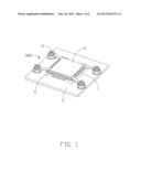
[0009] FIG. 2 is a side view of the electrical connector assembly as shown in FIG. 1;
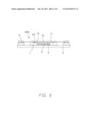
[0010] FIG. 3 is an exploded view of the electrical connector assembly shown in FIG. 1;
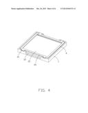
[0011] FIG. 4 is isometric, assembled view of the electrical connector shown in FIG. 1;
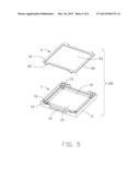
[0012] FIG. 5 is an exploded view of the electrical connector show in FIG. 1; and
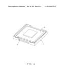
[0013] FIG. 6 is an isometric view of the electrical connector that the chip module assembled thereof show in FIG. 1.
DESCRIPTION OF PREFERRED EMBODIMENT
[0014] Reference will now be made to the drawings to describe the present invention in detail.
[0015] Referring to FIGS. 1-6, an electrical connector 1000 according to the present invention comprises a printed circuit board 3, an electrical connector 100 assembled to the printed circuit board 3, a chip module 2 assembled to the electrical connector 100 and a fixing device (not show) fixing the electrical connector 100 along with the chip module 2 to the printed circuit board 3. The electrical connector 100 comprises an insulative housing 1, a plurality of terminals (not show) retained therein and a retaining block 4 assembled at the insulative housing 1. The fixing device comprises a pressing element 5 for pressing the chip module 2 and a plurality of screws 6 fixing the chip module 2 to the printed circuit board 3.
[0016] Referring to FIG. 5, the insulative housing 1 comprises a bottom wall 10 and four side walls 11 extending upwardly from the bottom wall 10. The side walls 11 have a plurality of slots 14 cooperated with the block 4. The bottom wall 10 has a plurality of receiving holes 13 for receiving the terminals. Each of a pair of side walls 11 has a breach 12 respectively. The breach 12 is configured with inverted trapezoidal shape and located in the middle of the side wall 11. Between the bottom wall 10 and the side walls 11 forms a receiving space 15 to receive the chip module 2 for assembling the chip module 2 from top to bottom in a vertical direction. Near the corners of the side walls 11 have a plurality of leading portions 16 protruding to the receiving space 15 for leading the chip module 2 to assemble to the insulative housing 1, the leading portions 11 prevents the chip module 2 from moving in a horizontal direction perpendicular to the vertical direction.
[0017] The block 4 is configured with a frame shape and the block 4 has an open 43. The block 4 comprises a base 40, a plurality of extending portions 41 extending outwardly from the base 40 and a plurality of tabs 42 protruding to the insulative housing 1. The extending portion 41 located near a corner of the base 40.
[0018] Referring to FIG. 3, the chip module 2 is step shaped and comprises a substrate 20 and a die 21 protruding from a middle of the substrate 20. The bottom surface of the substrate 20 has a plurality of pads (not show) to contact with the terminals for electrically connecting the chip module 2 to the electrical connector 100. The printed circuit board 3 is flat plate and it comprises a plurality of retention portions 31. The pressing element 5 is configured with X shaped and it comprises a flat body portion 50, a plurality of connecting portions 51 extending outwardly from at least four corners of the body portion 50. Each of the ends of the connecting portions 51 have a through hole 52 for receiving the screws 6. The screws 6 cooperate with the retention portions 31 of the printed circuit board 3.
[0019] When assembling the electrical connector assembly, first assembled the chip module 2 to the insulative housing 1, then assembled the block 4 to the insulative housing 1 and the block 4 pressed the chip module 2, but the pressure of the block 4 is so small that it can not achieve the stable electrically connection between the electrical connector 100 and the chip module 2. The block 4 can prevent the chip module 2 coming off from the insulative housing 1 through the interference of the tabs 42 and the slots 14.
[0020] Referring to FIGS. 1-2, after assembling the electrical connector assembly 1000, the pressing element 5 is fixed to the printed circuit board 3 by the screws 6. The body portion 50 presses the chip module 2 and it provides the pressing force for the chip module 2 and achieve the stable electrically connection of the chip module 2 and the electrical connector 100. The height of the block 4 is smaller than the height of the die 21 of the chip module 2. So, after assembling the block 4 to the insulative housing 1, the block 4 can not be removed until the pressing element 5 fixed to the printed circuit board 3. The height of the block 4 that assembled to the insulative housing 1 is equal to the height of the side walls 11.
[0021] After the chip module 2 received in the receiving space 15, the block 4 can prevent the chip module 2 coming off from the insulative housing 1 while the chip module 2 assembled to the insulative housing 1 and not fixed to the printed circuit board 3, and it can prevent the damage of the chip module 2 and offsetting of the chip module 2.
[0022] Although the present invention has been described with reference to particular embodiments, it is not to be construed as being limited thereto. Various alterations and modifications can be made to the embodiments without in any way departing from the scope or spirit of the present invention as defined in the appended claims.
User Contributions:
Comment about this patent or add new information about this topic:
Images included with this patent application:
 |  |
 |  |
 |  |
 |
| Similar patent applications: | |
| Date | Title |
|---|---|
| 2014-04-03 | Electrical connector with new insert-molding method for terminal retaining |
| 2014-04-03 | Flat cable waterproofing connector and waterproofing connector structure for flat cable |
| 2014-04-03 | Coaxial cable connector assembly and a receptor connector |
| 2014-04-03 | Electrical socket assembly and method of manufacturing same |
| 2014-04-03 | Compressible pin assembly having frictionlessly connected contact elements |
| New patent applications in this class: | |
| Date | Title |
|---|---|
| 2019-05-16 | Socket connector for an electronic package |
| 2019-05-16 | Socket connector assembly for an electronic package |
| 2016-07-07 | Electrical connector assembly with holding member |
| 2016-03-24 | Card connector and electronic device including the same |
| 2016-01-07 | Looped socket pin |
| New patent applications from these inventors: | |
| Date | Title |
|---|---|
| 2016-05-19 | Electrical connector for use with cradle |
| 2016-05-19 | Machine case with improved electrical connector |
| 2016-05-19 | Machine case with improved terminal module |
| 2016-04-21 | Optical module with glass slide |
| 2016-04-21 | Optical module assembly with improved printed circuit board |
| Top Inventors for class "Electrical connectors" | |
| Rank | Inventor's name |
|---|---|
| 1 | Jerry Wu |
| 2 | Noah Montena |
| 3 | Qi-Sheng Zheng |
| 4 | Jun Chen |
| 5 | Norman R. Byrne |