Patent application title: CURRENT-MODE CMOS LOGARITHMIC FUNCTION CIRCUIT
Inventors:
Karama M. Al-Tamimi (Dhahran, SA)
Munir Ahmed Al-Absi (Dhahran, SA)
Assignees:
KING FAHD UNIVERSITY OF PETROLEUM AND MINERALS
IPC8 Class: AH03F345FI
USPC Class:
330253
Class name: With semiconductor amplifying device (e.g., transistor) including differential amplifier having field effect transistor
Publication date: 2013-09-12
Patent application number: 20130234796
Abstract:
The current-mode CMOS logarithmic function circuit provides an ultra-low
power circuit that produces an output current proportional to the
logarithm of the input current. An OTA (operational transconductance
amplifier) constructed from CMOS transistors, in combination with two
PMOS transistors configured in weak inversion mode for providing a
reference voltage input and a voltage input from the input current to the
OTA, provides the circuit with a high dynamic range, controllable
amplitude, high accuracy, and insensitivity to temperature variation.Claims:
1. A current-mode CMOS logarithmic function circuit, comprising: an
operational transconductance amplifier (OTA) having an inverting voltage
input, a non-inverting voltage input, and a current output; a first
MOSFET adapted for receiving a reference current, the first MOSFET being
configured in weak inversion mode and producing a voltage output
connected to the non-inverting input of the OTA; and a second MOSFET
adapted for receiving a current input, the second MOSFET being configured
in weak inversion mode and producing a voltage output connected to the
inverting input of the OTA; whereby the OTA produces an amplified current
at the current output proportional to the logarithm of the current input
when the reference current has a constant value.
2. The current-mode CMOS logarithmic function circuit according to claim 1, wherein said first and second MOSFETs comprise a pair of P-channel metal oxide semiconductors (PMO).
3. The current-mode CMOS logarithmic function circuit according to claim 1, wherein said OTA has semiconductors consisting of a plurality of complementary metal oxide semiconductor (CMOS) MOSFET transistors connected in a circuit for amplifying the current input to produce an amplified current at the current output proportional to the logarithm of the current input when the reference current has a constant value.
4. The current-mode CMOS logarithmic function circuit according to claim 1, further comprising a pair of CMOS transistors configured in a bias circuit connected to said OTA for providing a bias current for controlling amplitude of the current at the current output.
Description:
FIELD OF THE INVENTION
[0001] The present invention relates to signal processing circuits, and particularly to a current-mode CMOS logarithmic function circuit that produces an output current proportional to the logarithm of the input current.
DESCRIPTION OF THE RELATED ART
[0002] Nowadays, a significant increase in the use of CMOS technology for realization of analog circuits has been observed. Current-mode circuits have received more attention than their voltage-mode counterparts. CMOS circuits with nonlinear functions will greatly enhance signal processing capabilities, such as clock recovery, waveform generation, adaptive filtering etc, Logarithmic function circuits produce an output that is proportional to the logarithm of the input. These types of circuits are used in applications that require compression of analog input data, linearization of transducers that have exponential outputs, and analog multiplication and division. Logarithmic functions are also widely used in many signal processing applications.
[0003] However, conventional logarithmic function circuits suffer from a number of limitations, including the absence of low voltage operation capacity, limited dynamic range, etc. Thus, a current-mode CMOS logarithmic function circuit solving the aforementioned problems is desired.
SUMMARY OF THE INVENTION
[0004] The current-mode CMOS logarithmic function circuit provides an ultra-low power circuit that produces an output current proportional to the logarithm of the input current. An operational transconductance amplifier (OTA) in combination with two P-channel metal oxide semiconductor (PMOS) transistors provides a high dynamic range, controllable amplitude, high accuracy, and insensitivity to temperature variation
[0005] These and other features of the present invention will become readily apparent upon further review of the following specification and drawings.
BRIEF DESCRIPTION OF THE DRAWINGS
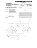
[0006] FIG. 1 is a partial schematic diagram of a current-mode CMOS logarithmic function circuit according to the present invention.
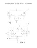
[0007] FIG. 2 is a detailed schematic diagram of a current-mode CMOS logarithmic function circuit according to the present invention.
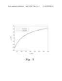
[0008] FIG. 3 is a plot of output current as a function of input current generated by an HSPICE simulation of the circuit of FIGS. 1 and 2.
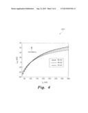
[0009] FIG. 4 is a plot of output current vs. input current generated by an HSPICE simulation of the circuit of FIGS. 1 and 2 for different bias currents.
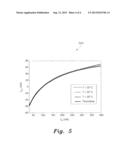
[0010] FIG. 5 is a plot of output current vs. input current generated by an HSPICE simulation of the circuit of FIGS. 1 and 2 for different operating temperatures.
[0011] Similar reference characters denote corresponding features consistently throughout the attached drawings.
DETAILED DESCRIPTION OF THE PREFERRED EMBODIMENTS
[0012] The current-mode CMOS logarithmic function circuit provides an ultra-low power circuit that produces an output current proportional to the logarithm of the input current. An OTA (operational transconductance amplifier) in combination with two PMOS transistors provides a high dynamic range, controllable amplitude, high accuracy and insensitivity to temperature variation.
[0013] Although theoretically or ideally there should be no current between the drain and source of a MOSFET when the transistor is turned off (the gate-to-source voltage is less than the threshold voltage of the device), in practice there is a weak inversion current that varies exponentially with the gate-to-source bias voltage. This is referred to herein as operation in the weak inversion mode. The current-mode CMOS logarithmic function circuit makes use of this phenomenon to produce an output current proportional to the logarithm (natural logarithm) of the input current.
[0014] The PMOS transistors M5 and M6 are configured with OTA 12 as shown in FIG. 1. It is well known that the output current of the OTA is given by:
Iout=gm(V1-V2) (1)
where gm is the transconductance of the MOS (metal oxide semiconductors) used in the OTA, and V1 and V2 are the two input voltages. Transistors M5 and M6 are biased in the weak inversion mode and used to convert current Ix (a reference current) and Iin (the input current) to voltages V1 and V2, respectively, as follows:
V 1 = V DD - V SG 5 = V DD - nv t ln ( I x I Do ) ( 2 ) V 2 = V DD - V SG 6 = V DD - nv t ln ( I i n I Do ) ( 3 ) ##EQU00001##
where VDD is the supply voltage and VSG is the gate-to-source voltage, vt is the thermal voltage, n is the slop factor and IDo is the leakage current of the MOSFET. As shown in FIG. 1, the voltage V1 generated by the reference current is connected to the non-inverting input of the OTA 12, and the voltage V2 generated by the input current is connected to the inverting input of the OTA 12. Combining equations (2) and (3) yields:
ln ( I i n I x ) = ( V 1 - V 2 nv t ) ( 4 ) ##EQU00002##
[0015] Combining equations (4) and (1), the output current Iout is given by:
I out = g m nv t ln ( I i n I x ) ( 5 ) ##EQU00003##
[0016] The transconductance of the MOSFET transistor in weak inversion is given by:
g m = I D nv t ( 6 ) ##EQU00004##
where ID is the bias current of the MOSFET and is given by Ibias/2. From (5) and (6), the output current can be rewritten as:
I out = I D ln ( I i n I x ) ( 7 ) ##EQU00005##
[0017] With reference to equation (7) if the reference current Ix is kept constant, the output current is proportional to the logarithm of the input current Iin. The amplitude of the output current can be controlled by the bias current ID of the OTA 12. The complete circuit diagram of the invention is shown in FIG. 2. Transistors M1-M4 form the OTA 12. Transistors M1-M4 are CMOS transistors. The OTA 12 avoids the use of bipolar semiconductors, and the use of only CMOS semiconductors reduces power consumption, enabling low voltage operation. Transistors M7 and M8 are CMOS transistors that provide the required bias current.
[0018] The functionality of the circuit was carried out using HSPICE 0.35 um technology. The output current was measured by forcing it through a grounded load resistor RL=10 kΩ. The results obtained with ISS=100 nA (i.e., ID=50 nA), Ix=100 nA and VDD=-VSS=0.5V are shown in plot 300 of FIG. 3. Plot 300 shows that the simulated results are in excellent agreement with the required function, thereby confirming the functionality of the circuit.
[0019] Simulation was carried out for different bias currents (ID=40, 45 and 50 nA) and different temperatures (T=20, 25 and 30° C.). Simulation results are shown in plot 400 of FIG. 4 and plot 500 of FIG. 5.
[0020] It is to be understood that the present invention is not limited to the embodiments described above, but encompasses any and all embodiments within the scope of the following claims.
User Contributions:
Comment about this patent or add new information about this topic:
| People who visited this patent also read: | |
| Patent application number | Title |
|---|---|
| 20130273325 | CORRUGATED INTERFACES FOR MULTILAYERED INTERCONNECTS |
| 20130273324 | STRENGTHENED GLASS ARTICLES HAVING ETCHED FEATURES AND METHODS OF FORMING THE SAME |
| 20130273323 | INTERIOR PART FOR VEHICLE AND METHOD FOR TREATING EDGE THEREOF |
| 20130273322 | DEVICE FOR EMBOSSING FOILS |
| 20130273321 | VARIABLE TEXTURE FLOOR COVERING |
Images included with this patent application:
 |  |
 |  |
 |  |
 |
| Similar patent applications: | |
| Date | Title |
|---|---|
| 2014-05-22 | Distortion compensating apparatus, transmitter, distortion compensating method, and transfer function calculating method |
| 2014-04-10 | Automatic gain control circuit |
| 2014-05-22 | Systems and methods for band-limited adaptation for pa linearization |
| 2009-03-19 | Current mirror circuit |
| 2014-04-10 | Offset current trim circuit |
| New patent applications in this class: | |
| Date | Title |
|---|---|
| 2016-06-23 | Low power operational transconductance amplifier |
| 2016-06-23 | Electronic devices and methods having a compact multi-way transformer combiner |
| 2016-06-16 | Low power operational transconductance amplifier |
| 2016-06-09 | Buffer circuit robust to variation of reference voltage signal |
| 2016-05-19 | High speed signal level detector and burst-mode trans impedance amplifier using the same |
| New patent applications from these inventors: | |
| Date | Title |
|---|---|
| 2015-10-08 | High dynamic range exponential current generator with mosfets |
| 2015-05-21 | Cmos logarithmic current generator and method for generating a logarithmic current |
| Top Inventors for class "Amplifiers" | |
| Rank | Inventor's name |
|---|---|
| 1 | Nadim Khlat |
| 2 | Ahmadreza Rofougaran |
| 3 | Sehat Sutardja |
| 4 | Yoo Sam Na |
| 5 | David F. Sorrells |