Patent application title: PRINTED CIRCUIT BOARD
Inventors:
Yung-Chieh Chen (Tu-Cheng, TW)
Shou-Kuo Hsu (Tu-Cheng, TW)
Assignees:
HON HAI PRECISION INDUSTRY CO., LTD.
IPC8 Class: AH05K700FI
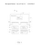
USPC Class:
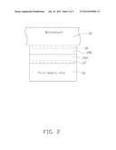
361783
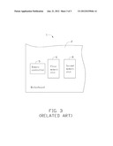
Class name: Printed circuit board connection of components to board having semiconductive device
Publication date: 2012-06-21
Patent application number: 20120155046
Abstract:
A printed circuit board (PCB) includes a top layer, a memory controller,
two gaps, and two connectors. The memory controller is located on the top
layer. A number of golden fingers are respectively set on the top layer
near each gap and electrically connected to the memory controller. Each
connector includes a first slot to hold the gold fingers near a
corresponding one of the gaps and a second slot to hold a number of gold
fingers of a corresponding one of two memory chips. The first slot is
electrically connected to the second slot. Each memory chip and the PCB
are coplanar.Claims:
1. A printed circuit board (PCB) comprising: a top layer defining a first
gap and a second gap extending through the PCB, the top layer comprising
a plurality of first golden fingers near the first gap, and a plurality
of second golden fingers near the second gap; a memory controller located
on the top layer, and electrically connected to the plurality of first
and second golden fingers; a first connector comprising a first slot to
hold the plurality of first golden fingers near the first gap and a
second slot to hold a plurality of third golden fingers of a first memory
chip, wherein the first slot is electrically connected to the second
slot, the first memory chip and the PCB are coplanar; and a second
connector comprising a third slot to hold the plurality of second golden
fingers near the second gap and a fourth slot to hold a plurality of
fourth golden fingers of a second memory chip, wherein the third slot is
electrically connected to the fourth slot, the second memory chip and the
PCB are coplanar.
2. The PCB of claim 1, wherein a length of the first gap is equal to a length of the first memory chip.
3. The PCB of claim 1, wherein a length of the second gap is equal to a length of the second memory chip.
4. The PCB of claim 1, wherein a distance between the plurality of first golden fingers and the memory controller is equal to a distance between the plurality of second golden fingers and the memory controller.
Description:
CROSS-REFERENCE TO RELATED APPLICATION
[0001] Relevant subject matter is disclosed in a pending U.S. patent application (Attorney Docket No. US36485) having the same title, which is assigned to the same assignee as named herein.
BACKGROUND
[0002] 1. Technical Field
[0003] The present disclosure relates to a printed circuit board (PCB).
[0004] 2. Description of Related Art
[0005] Referring to FIG. 3, on a conventional motherboard 1, a first memory slot 6 and a second memory slot 8, which make up dual-channel memories, are located on a top layer 2 of the motherboard 1. The memory slots 6 and 8 are horizontal slots to reduce the thickness of the motherboard 1 with two memories plugged into the memory slots 6 and 8. However, the memories projects from the motherboard and increases the height occupied by the motherboard 1. In addition, the first memory slot 6 and the second memory slot 8 are set on a side of a memory controller 5. As a result, a distance between the first memory slot 6 and the memory controller 5 is different from a distance between the second memory slot 8 and the memory controller 5. Therefore, the traces between the memory slots 6 and 8 and the memory controller 5 need to be designed at different lengths and according to different rules, making the design process overly-complex.
BRIEF DESCRIPTION OF THE DRAWINGS
[0006] Many aspects of the present embodiments can be better understood with reference to the following drawings. The components in the drawings are not necessarily drawn to scale, the emphasis instead being placed upon clearly illustrating the principles of the present embodiments. Moreover, in the drawings, like reference numerals designate corresponding parts throughout the several views.
[0007] FIG. 1 is a schematic, exploded diagram of an exemplary of a printed circuit board.
[0008] FIG. 2 is an enlarged, schematic diagram of a connector mounted to the printed circuit board of FIG. 1.
[0009] FIG. 3 is a schematic diagram of a conventional motherboard.
DETAILED DESCRIPTION
[0010] The disclosure, including the accompanying drawings, is illustrated by way of example and not by way of limitation. It should be noted that references to "an" or "one" embodiment in this disclosure are not necessarily to the same embodiment, and such references mean at least one.
[0011] Referring to FIG. 1, an exemplary embodiment of a printed circuit board (PCB) includes a top layer 11 and other layers (not shown). A memory controller 12 is located on the top layer 11. In the embodiment, the PCB is a motherboard 10.
[0012] The motherboard 10 defines a first gap 15 and a second gap 25 therein through the top layer 11 and the other layers. A length of the first gap 15 is equal to a length of a first memory chip 16. A length of the second gap 25 is equal to a length of a second memory chip 26. A plurality of golden fingers 18 and 28 are set on the top layer 11 of the motherboard 10, respectively near the first gap 15 and the second gap 25. The golden fingers 18 and 28 are electrically connected to the memory controller 12 through traces on the motherboard 10. A distance between the memory controller 12 and the golden fingers 18 is equal to a distance between the memory controller 12 and the golden fingers 28.
[0013] Also referring to FIG. 2, in the embodiment, a first connector 19 includes a first memory slot 190 and a second memory slot 192 electrically connected to each other. The first memory slot 190 is configured to hold the golden fingers 18 near the first gap 15. The second memory slot 192 is configured to hold the golden fingers 17 of the first memory chip 16. Because the first memory slot 190 is electrically connected to the second memory slot 192, the memory controller 12 can communicate with the first memory chip 16 through the golden fingers 18 near the first gap 15 and the first connector 19. Moreover, when the first memory chip 16 is plugged into the second memory slot 192, the first memory chip 16 and the motherboard 10 are coplanar.
[0014] A first memory slot of a second connector 29 is configured to hold the golden fingers 28 near the second gap 25. A second memory slot of the second connector 29 is configured to hold golden fingers 27 of a second memory chip 26. Moreover, when the second memory chip 26 is plugged into the second memory slot of the second connector 29, the second memory chip 26 and the motherboard 10 are coplanar. As a result, a thickness of the motherboard 10 including the first memory chip 16 and the second memory chip 26 is same with the thickness of the motherboard 10. In addition, the motherboard 10 can install different memories with different capacity. Moreover, the first memory chip 16 and the second memory chip 26 make up dual-channel memories.
[0015] Because the distance between the golden fingers 18 near the first gap 15 and the memory controller 12 is equal to the distance between the golden fingers 28 near the second gap 25 and the memory controller 12, traces between the golden fingers 18 and 28, and the memory controller 12 can be designed to be the same length and according to the same rules. In the embodiment, the distance between the golden fingers 18 and the memory controller 12 can be regarded as a distance between a center of the golden fingers 18 and a center of the memory controller 12. The distance between the golden fingers 28 and the memory controller 12 can be regarded as a distance between a center of the golden fingers 28 and the center of the memory controller 12.
[0016] The foregoing description of the exemplary embodiments of the disclosure has been presented only for the purposes of illustration and description and is not intended to be exhaustive or to limit the disclosure to the precise forms disclosed. Many modifications and variations are possible in light of the above everything. The embodiments were chosen and described in order to explain the principles of the disclosure and their practical application so as to enable others of ordinary skill in the art to utilize the disclosure and various embodiments and with various modifications as are suited to the particular use contemplated. Alternative embodiments will become apparent to those of ordinary skills in the art to which the present disclosure pertains without departing from its spirit and scope. Accordingly, the scope of the present disclosure is defined by the appended claims rather than the foregoing description and the exemplary embodiments described therein.
User Contributions:
Comment about this patent or add new information about this topic:
Images included with this patent application:
 |  |
 |  |
| Similar patent applications: | |
| Date | Title |
|---|---|
| 2010-02-25 | Printed circuit board |
| 2010-05-13 | Printed circuit board |
| 2010-09-02 | Printed circuit board |
| 2010-09-09 | Printed circuit board unit |
| 2010-12-23 | Printed circuit board |
| New patent applications in this class: | |
| Date | Title |
|---|---|
| 2016-09-01 | Multilayer wiring board |
| 2016-07-14 | Printed circuit board, package and method of manufacturing the same |
| 2016-06-30 | Semiconductor device |
| 2016-06-23 | Method for contacting and rewiring an electronic component embedded into a printed circuit board |
| 2016-06-23 | Electronic packages with pre-defined via patterns and methods of making and using the same |
| New patent applications from these inventors: | |
| Date | Title |
|---|---|
| 2015-05-21 | Printed circuit board |
| 2014-10-16 | System and method for checking signal transmission line |
| 2014-09-11 | Control system and method for server |
| 2014-08-21 | Storage expansion system |
| 2014-07-31 | Data center and power supply system thereof |
| Top Inventors for class "Electricity: electrical systems and devices" | |
| Rank | Inventor's name |
|---|---|
| 1 | Zheng-Heng Sun |
| 2 | Levi A. Campbell |
| 3 | Li-Ping Chen |
| 4 | Robert E. Simons |
| 5 | Richard C. Chu |