Patent application title: Touch Screen and Manufacturing Method Thereof
Inventors:
Gap Young Kim (Seoul, KR)
Hyun Min Na (Seoul, KR)
Hyuk Jin Hong (Seoul, KR)
Hyuk Jin Hong (Seoul, KR)
Assignees:
LG INNOTEK CO., LTD.
IPC8 Class: AG06F3041FI
USPC Class:
345173
Class name: Computer graphics processing and selective visual display systems display peripheral interface input device touch panel
Publication date: 2011-12-15
Patent application number: 20110304568
Abstract:
A touch screen according to an embodiment of the present invention
includes: a transparent conductive material deposited on a top surface of
a flexible plastic film; and a metal layer vacuum-deposited on the
transparent conductive film. According to the embodiment of the present
invention, the touch screen capable of providing the excellent
flexibility and simplifying the manufacturing process, and the method of
manufacturing the same can be provided.Claims:
1. A touch screen, characterized by: a transparent conductive material
deposited on a top surface of a flexible plastic film; and a metal layer
vacuum-deposited on the transparent conductive film.
2. The touch screen according to claim 1, characterized in that the flexible plastic film includes at least any one of PET, PES, PC, PE, PI, and Acryl.
3. The touch screen according to claim 1, characterized in that the metal layer includes a conductor layer made of at least any one of Ag, Cu, Au, and Al.
4. The touch screen according to claim 1, characterized in that the metal layer includes: at least any one of Ni, Cr, Ni-Cr, Ti, Sn, and Mo; a conductor layer made of at least any one of Ag, Cu, Au, and Al.
5. The touch screen according to claim 1, characterized in that the metal layer is vacuum-deposited using at least any one of RF sputter, DC sputter, and CVD technologies.
6. A method of manufacturing a touch screen, characterized by: performing heat treatment for preventing an ITO film from shrinking; removing and pre-processing impurities on a surface of the ITO film; and depositing a metal layer on the pre-processed ITO film
7. The method according to claim 6, wherein the step of removing and pre-processing of impurities on the surface of the ITO film includes generating and pre-processing ion beams using at least any one of O2, O3, N2, N2O, NO2, and CO.sub.2.
8. The method according to claim 6, wherein the step of removing and pre-processing of the impurities on the surface of the ITO film includes generating and pre-processing plasma using at least any one of Ar, Kr, Xe, and Ne.
9. The method according to claim 6, wherein the step of vacuum depositing of the metal layer on the pre-processed ITO film includes forming a conductor layer by vacuum-depositing at least any one of Ag, Cu, Au, and Al.
10. The method according to claim 6, wherein the step of depositing of the metal layer on the pre-processed ITO film includes: forming a buffer layer by vacuum-depositing at least any one of Ni, Cr, Ni-Cr, Ti, Sn, and Mo; and forming a conductor layer by vacuum-depositing at least any one of Ag, Cu, Au, and Al.
11. The method according to claim 6, wherein the step of vacuum depositing of a metal layer on the pre-processed ITO film includes vacuum-depositing using at least any one of RF sputter, DC sputter, and CVD technologies.
Description:
TECHNICAL FIELD
[0001] The present invention relates to a touch screen and a method of manufacturing the same.
BACKGROUND ART
[0002] A touch screen is a device detecting approached or touched positions of fingers or a touch pen. The touch screen may be mounted on a screen of a video display device to easily input information.
[0003] The touch screen uses a transparent electrode to detect a touch input by fingers or a pen. The transparent electrode may be formed by wiring a metal layer on a transparent conductive oxide film such as indium tin oxide (ITO).
[0004] Generally, a screen printing technology of printing and drying metal wirings has been used to form wirings on the ITO film.
[0005] However, there is a problem in that the touch screen wiring process according to the related art is complicated. In addition, the touch screen wiring process according to the related art may make thickness of a metal layer thick. If the metal layer is thick, there are problems in that flexibility of the touch screen is weakened and the adhesion thereof is reduced.
DISCLOSURE OF INVENTION
[0006] An embodiment of the present invention is to provide a touch screen capable of providing excellent flexibility and simplifying a manufacturing process, and a method of manufacturing the same.
[0007] In an embodiment of the present invention, a touch screen is provided, the touch screen characterized by: a transparent conductive material deposited on a top surface of a flexible plastic film; and a metal layer vacuum-deposited on the transparent conductive
[0008] In another embodiment of the present invention, a method of manufacturing a touch screen is provided, the method characterized by: performing heat treatment for preventing an ITO film from shrinking; removing and pre-processing impurities on a surface of the ITO film; and depositing a metal layer on the pre-processed ITO film.
ADVANTAGEOUS EFFECTS
[0009] According to the embodiment of the present invention, the touch screen and the method of manufacturing the same capable of providing the excellent flexibility and simplifying the manufacturing process can be provided.
BRIEF DESCRIPTION OF DRAWINGS
[0010] The above and other objects and features of the present invention will become apparent from the following description of preferred embodiments taken in conjunction with the accompanying drawings.
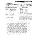
[0011] FIG. 1 is a cross-sectional view of a touch screen according to a first embodiment of the present invention;
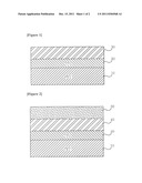
[0012] FIG. 2 is a cross-sectional view of a touch screen according to a second embodiment of the present invention; and
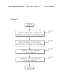
[0013] FIG. 3 is a flow chart of a method of manufacturing a touch screen according to an embodiment of the present invention.
DETAILED DESCRIPTION
[0014] Hereinafter, a touch screen and a method of manufacturing the same according to an embodiment of the present invention will be described in detail with reference to the accompanying drawings. However, if it is determined that the detailed description of relevant known functions or components makes subject matters of the present invention obscure, the detailed description thereof will be omitted.
[0015] FIG. 1 is a cross-sectional view of a touch screen according to a first embodiment of the present invention.
[0016] As shown in FIG. 1, the touch screen according to the first embodiment of the present invention includes a transparent conductive film 20 such as indium tin oxide, or the like, that is deposited on a top surface of the flexible plastic film 10 and a conductor layer 30 that is deposited on a transparent conductive film 20.
[0017] The flexible plastic film 10 may use a film made of PES, PC, PE, PI, Acryl, or the like, as a base. The embodiment of the present invention illustrates a case in which a polyethylene terephthalate (PET) film 10 is used, In this case, the PET film 10 has shrinkage characteristics in a range of 100 to 150° C. When the PET film 10 on which the transparent conductive film 20 is deposited is used to manufacture the touch screen, there is a problem in that an align is mismatched due to the shrinkage of the PET film 10 at the time of performing heat treatment for a bonding process of upper and lower plates.
[0018] Therefore, it is preferable to remove the shrinkage that may occur during a metal layer deposition process and a post-process by performing an annealing process that heat-treats the PET film 10 at about 150° C. for 90 minutes to shrink the film in advance.
[0019] The conductor layer 30 is deposited on the ITO film 20. When the touch screen is operated in a resistive or capacitive type, the surface of the ITO film 20 serves to detect touch and the conductor layer 30 is used as an electrode moving charges. Therefore, the conductor layer 30 is formed using a conductive metal having a resistance value lower than that of the ITO film 20. The conductor layer 30 may be formed by depositing metals having excellent conductivity such as Ag, Cu, Au, Al, or the like using a vacuum deposition technology such as RF sputter, DC sputter, CVD , or the like. Since the conductor layer 30 directly affects the sensitivity of the touch screen, the deposition metal and the thickness may he controlled so that a resistance value may be controlled to 0.1Ωquadrature(square) or less.
[0020] Meanwhile, when the conductor layer 30 is deposited using the vacuum deposition technology, a pre-processing process of removing the impurities on the surface of the ITO film 20 using plasma or ion beams may be performed in order to improve the adhesion between the ITO film 20 and the conductor layer 30.
[0021] FIG. 2 is a cross-sectional view of a touch screen according to a second embodiment of the present invention.
[0022] As shown in FIG. 2, the touch screen according to the second embodiment of the present invention may be used as a buffer layer 40 and a conductor layer 30 by forming the metal layer on the ITO film 20 deposited on the PET film 10 in a double layer.
[0023] When the metal layers 30 and 40 are deposited, after the surface of the ITO film 20 is pre-processed using a method such as plasma processing or ion beam irradiation and then, the metal layers 30 and 40 are deposited, such that the damage to the surface of the ITO film 20 may be prevented and the adhesion and the conductivity of the metal layers 30 and 40 may be improved.
[0024] The buffer layer 40 directly deposited on the ITO film 20 improves the adhesion between the ITO film 20 and the metal layers 30 and 40. Therefore, the buffer layer 40 may use a material such as Ni, Cr, Ni-Cr, Ti, Sn, Mo, or the like and the conductor layer 30 may select a material having excellent adhesion and conductivity with the buffer layer 40.
[0025] The buffer layer 40 directly deposited on the ITO film 20 improves the adhesion between the ITO film 20 and the metal layers. Therefore, the buffer layer 40 may use a material such as Ni, Cr, Ni-Cr, Ti, Sn, Mo, or the like and the conductor layer 30 may select a material having excellent adhesion and conductivity with the buffer layer 40.
[0026] The design conditions of the buffer layer 40 and the conductor layer 3 and the corresponding adhesion and conductivity are as the following Table 1.
TABLE-US-00001 TABLE 1 Conductivity (Surface Conductor Resistance, Adhesion Buffer Layer Layer Ω/quadrature) (kgf/cm) Experiment 1 Mo, 100quadrature Ag, 800quadrature 1.50 0.95 Experiment 2 Ni--Cr, 100quadrature Ag, 800quadrature 1.48 0.98 Experiment 3 Ni--Cr, 100quadrature Cu, 1000quadrature 1.10 0.97 Experiment 4 0 Ag, 1000quadrature 0.88 0.3 Experiment 5 0 Cu, 1000quadrature 0.94 0.34
[0027] As listed in the above-mentioned [Table 1], the Mo/Ag deposition ITO film 20 may be formed by depositing Mo on the buffer layer 40 at a thickness of 100 A and Ag on the conductor layer 30 at a thickness of 800 A. In this case, the conductivity and the adhesion are measured as 1.50Ωquadrature, 0.95 kgf/cm.
[0028] Further, the Ni-Cr/Ag deposition ITO film 20 may be formed by depositing Ni-Cr on the buffer layer 40 at a thickness of 100 A and Ag on the conductor layer 30 at a thickness of 800 A. In this case, the conductivity and the adhesion are measured as 1.48 Ωquadrature, 0.98 kgf/cm.
[0029] The Ni-Cr/Cu deposition ITO film 20 may be formed by depositing Ni-Cr on the buffer layer 40 at a thickness of 100 A and Cu on the conductor layer 30 at a thickness of 1000 A. In this case, the conductivity and the adhesion are measured as 1.10Ωquadrature, 0.97 kgf/em.
[0030] Further, as shown in Experiment 4 and Experiment 5, when only the conductor layer 30 is formed, the conductivity and the adhesion are each measured as 0.88Ωquadrature, 0.3 kgf/cm and 0.94Ωquadrature, 0.34 kgf/cm.
[0031] As can be appreciated from the experimental results, when the buffer layer is formed, it can be appreciated that the adhesion may be remarkably improved.
[0032] FIG. 3 is a flow chart of a method of manufacturing a touch screen according to an embodiment of the present invention.
[0033] As shown in FIG. 3, when the touch screen is manufactured according to the embodiment of the present invention, the PET film 10 deposited with the ITO film 20 is heat-treated (S110 ).
[0034] The surface of the ITO film 20 is pre-processed by using the plasma or the ion beams (S120) in order to improve the adhesion of the metal layer. In this case, reactive gas for generating ion beams may be selected among O2, O3, N2, N2O, NO2, and CO2 and may be selected among inert gases such as Ar, Kr, Xe, and Ne. In addition, the reactive gas or the inert gas may be applied alone or in a mixing state. Further, the irradiation amount of the ion beams may he used within a range of 1×10¹⁵/cm2˜1×1018/cm2.
[0035] The first metal layer, the buffer layer 40 is deposited on the pre-processed ITO film 20 (S130). The buffer layer 40 may be formed by depositing a metal such as Ni, Cr, Ni-Cr, Ti, Sn, Mo, or the like by using a vacuum deposition method such as RF sputter, DC sputter, CVD technologies, or the like.
[0036] The second metal, the conductor layer 30 is deposited on the first metal layer (S140). The conductor layer 30 may he formed by depositing metals such as Ag, Cu, Au, Al, or the like using the vacuum deposition method such as RF sputter, DC sputter, CVD technologies , or the like.
[0037] While the invention will be described in conjunction with exemplary embodiments, it will be understood that present description is not intended to limit the invention to those exemplary embodiments. It will be apparent to those skilled in the art that various modifications and variation can be made in the present invention without departing from the spirit or scope of the invention. Thus, it is intended that the present invention cover the modifications and Variations of this invention, provided they come within the scope of the appended claims and their equivalents.
[0038] Industrial Applicability
[0039] The present invention can provide the touch screen capable of providing the excellent flexibility and simplifying the manufacturing process.
User Contributions:
Comment about this patent or add new information about this topic:
| People who visited this patent also read: | |
| Patent application number | Title |
|---|---|
| 20150353540 | AZAINDOLE DERIVATIVES AS INHIBITORS OF PROTEIN KINASES |
| 20150353539 | AZAINDOLE DERIVATIVES AS MULTI KINASE INHIBITORS |
| 20150353538 | COMPOUNDS AND THERAPEUTIC USES THEREOF |
| 20150353537 | BICYCLIC HETEROCYCLE COMPOUNDS AND THEIR USES IN THERAPY |
| 20150353536 | Complex targeting hepatitis B virus |
Images included with this patent application:
 |  |
 |
| New patent applications in this class: | |
| Date | Title |
|---|---|
| 2022-05-05 | Display device |
| 2022-05-05 | Steering switch device and steering switch system |
| 2022-05-05 | Method of detecting touch location and display apparatus |
| 2022-05-05 | Touch display device, touch driving circuit and touch driving method thereof |
| 2022-05-05 | Electronic device |
| New patent applications from these inventors: | |
| Date | Title |
|---|---|
| 2022-08-04 | Dc-dc converter |
| 2014-12-18 | Touch panel and manufacturing method thereof |
| 2014-11-27 | Electrode pattern of touch panel and method of manufacturing the same |
| 2014-01-23 | Touch panel and method for manufacturing the same |
| 2013-12-05 | Touch panel |
| Top Inventors for class "Computer graphics processing and selective visual display systems" | |
| Rank | Inventor's name |
|---|---|
| 1 | Katsuhide Uchino |
| 2 | Junichi Yamashita |
| 3 | Tetsuro Yamamoto |
| 4 | Shunpei Yamazaki |
| 5 | Hajime Kimura |