Patent application title: Precharge Voltage Supplying Circuit
Inventors:
Byeong Cheol Lee (Seoul, KR)
Sang Il Park (Icheon-Si, KR)
Sang Il Park (Icheon-Si, KR)
IPC8 Class: AG11C712FI
USPC Class:
365201
Class name: Static information storage and retrieval read/write circuit testing
Publication date: 2011-10-06
Patent application number: 20110242919
Abstract:
A precharge voltage supplying circuit comprises a transistor operating in
response to a control signal, wherein the transistor is connected between
a first node to which an internal voltage is supplied and a second node
to which a precharge voltage is supplied, and a resistance element
connected in parallel to the transistor between the first node and the
second node.Claims:
1-19. (canceled)
20. A precharge voltage supplying circuit, comprising: a transistor operating in response to a control signal, wherein the transistor is connected between a first node to which an internal voltage is supplied and a second node to which a precharge voltage is supplied; and a resistance element connected in parallel to the transistor between the first node and the second node.
21. The precharge voltage supplying circuit of claim 20, wherein the precharge voltage is supplied to a pair of bit lines in response to a bit line equalizing control signal.
22. The precharge voltage supplying circuit of claim 20, wherein the precharge voltage is produced by a voltage drop across the resistance element or by a voltage drop across the transistor which is turned on in response to the control signal.
23. A precharge voltage supplying circuit, comprising: a transistor operating in response to a control signal, wherein the transistor is connected between a first node to which an internal voltage is supplied and a second node to which a precharge voltage is supplied; and a resistance element connected in series to the transistor between the first node and the second node.
24. The precharge voltage supplying circuit of claim 23, wherein the precharge voltage is supplied to a pair of bit lines in response to a bit line equalizing control signal.
25. The precharge voltage supplying circuit of claim 26, further comprising: wherein the logic unit includes a NOR gate for a NOR operation of a ground voltage signal and the test mode signal.
26. The precharge voltage supplying circuit of claim 23, further comprising: a logic unit configured to receive a test mode signal and produce an enable signal; and a switching element for connecting the first and second nodes in response to the enable signal from the logic unit.
27. The precharge voltage supplying circuit of claim 23, wherein the switching element is a NMOS transistor connected between the first node and the second node.
28. The precharge voltage supplying circuit of claim 20, further comprising: a logic unit configured to receive a test mode signal and produce an enable signal; and a switching element for connecting the first and second nodes in response to the enable signal from the logic unit.
29. The precharge voltage supplying circuit of claim 28, wherein the logic unit includes a NOR gate for a NOR operation of a ground voltage signal and the test mode signal.
30. The precharge voltage supplying circuit of claim 29, wherein the switching element is a NMOS transistor connected between the first node and the second node.
Description:
CROSS REFERENCE TO RELATED APPLICATIONS
[0001] This application is a divisional of U.S. application Ser. No. 12/005,706 filed Dec. 28, 2007, claiming priority to Korean application numbers 10-2007-0026584 and 10-2007-0063927, filed on Mar. 19, 2007, and Jun. 27, 2007, respectively, the entire contents of each of which are incorporated herein by reference.
BACKGROUND
[0002] Recently, the capacity of semiconductor memory devices is rapidly becoming larger and studies on methods to increase an operational speed and reduce current consumption are steadily conducted. Particularly, techniques to reduce the current consumption are developed in a semiconductor memory device which can be embedded in a portable system such as a cellular phone or a notebook computer.
[0003] One of the above mentioned techniques is to minimize the current consumption in a core area of a memory. The core area having a plurality of memory cells, bit lines and word lines is designed according to a critical design rule. Thus, the memory cells can be very small and operate with a low power consumption.
[0004] Particularly, a bit line precharge technique is important to increase the speed of a cell data access. The bit line precharge technique precharges a bit line (BL) to a half level of a core voltage (VCORE) before the data access in order to increase the speed of the data access.
[0005] Meanwhile, in a standby state, a potential difference occurs between a word line (WL) of 0V and a precharged bit line (BL). If a bridge occurs between the word line (WL) and the bit line (BL), a current consumption increases due to the bridge current which is caused by the potential difference. Therefore, in order to reduce the current consumption caused by the bridge current, a precharge voltage supplying circuit, which has a bleeder resistance, is used to generate a precharge voltage (VBLP) on the bit line where a voltage drop occurs.
SUMMARY
[0006] In an exemplary embodiment, a precharge voltage supplying circuit comprises a transistor operating in response to a control signal, wherein the transistor is connected between a first node to which an internal voltage is supplied and a second node to which a precharge voltage is supplied; and a resistance element connected in parallel to the transistor between the first node and the second node.
[0007] In another exemplary embodiment, a precharge'voltage supplying circuit comprises a transistor operating in response to a control signal, wherein the transistor is connected between a first node to which an internal voltage is supplied and a second node to which a precharge voltage is supplied; and a resistance element connected in series to the transistor between the first node and the second node.
BRIEF DESCRIPTION OF THE DRAWINGS
[0008] The above and other aspects, features and other advantages will be more clearly understood from the following detailed description taken in conjunction with the accompanying drawings, in which:
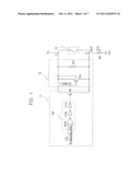
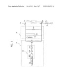
[0009] FIG. 1 is a circuit diagram of a precharge voltage supplying circuit according to an embodiment of the present disclosure.
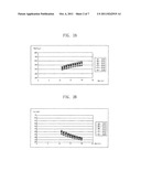
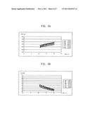
[0010] FIGS. 2A and 2B are graphs illustrating a precharge voltage characteristic and a bridge current characteristic, respectively, in the circuit of FIG. 1.
[0011] FIG. 3 is a circuit diagram of a precharge voltage supplying circuit according to another embodiment of the present disclosure.
DESCRIPTION OF EXEMPLARY EMBODIMENTS
[0012] Hereinafter, embodiments of the present invention will be described with reference to accompanying drawings. However, the embodiments are for illustrative purposes only and are not intended to limit the scope of the invention.
[0013] FIG. 1 is a circuit diagram of a precharge voltage supplying circuit according to an embodiment of the present disclosure.
[0014] Referring to FIG. 1, the precharge voltage supplying circuit includes a first switch unit 31, a bleeder resistance unit 32 and a second switch unit 34 which connects node C to node D.
[0015] The first switch unit 31 includes a logic unit 300 and an NMOS transistor N30 which is connected between node C and node D and is turned on in response to an output signal of the logic unit 300. The logic unit 300 includes a NOR gate NR30 receiving a test mode signal TM_BLEEDER_PWDD and a ground voltage VSS to perform a NOR operation, and inverters IV30 and IV31. Here, it is desirable to design the NMOS transistor N30 to have a large size.
[0016] The bleeder resistance unit 32 includes an NMOS transistor N31 which is connected between node C to which the internal voltage Vp is supplied and node D to which the precharge voltage VBLP is supplied and operates in response to the control signal BLEEDER_S, and a resistance element R30 which is in parallel connected to the NMOS transistor N31 between node C and node D.
[0017] Operation of the precharge voltage supplying circuit of FIG. 1 will be described below in detail.
[0018] The bleeder resistance unit 32 operates in accordance with the test mode signal TM_BLEEDER_PWDD. First, in a case that the test mode signal TM_BLEEDER_PWDD is in a low level, the output signal of the logic unit 300 is in a high level and the NMOS transistor N30 is turned on. Since the size of the NMOS transistor N30 is large, the voltage drop between node C and node D through the turn-on resistance of the NMOS transistor N30 is not so large. Thus, the precharge voltage VBLP, having a level which is almost the same as the internal voltage Vp, is output to node D. At this time, there is almost no voltage drop through the bleeder resistance unit 32 which includes the NMOS transistor N31 and the resistance element R30. Also, if the second switch unit 34 is turned on so that node C is connected to node D, operations of the NMOS transistor N31 and the bleeder resistance unit 32 are bypassed, and the precharge voltage VBLP, having a level which is almost the same as the internal voltage Vp, is output through node D.
[0019] Meanwhile, in a case that the test mode signal TM_BLEEDER_PWDD is in a high level, the output signal of the logic unit 300 is in a low level and the NMOS transistor N30 is turned off. Thus, a voltage drop of the internal voltage Vp occurs through the bleeder resistance unit 32 so that a voltage-dropped signal is output as the precharge voltage VBLP through node D. At this time, since the bleeder resistance unit 32 includes the NMOS transistor N31 and the resistance element R30, the second bit line precharge voltage VBLP is adjustable in various levels according to a PVT fluctuation and the range in the fluctuation is not so large. This is due to the characteristic of the NMOS transistor N31, which has various turn-on resistance values according to the PVT fluctuation, and the characteristic of the resistance element R30, which has a constant resistance value regardless of the PVT characteristic change.
[0020] Referring to FIG. 2A, although the precharge voltage VBLP, corresponding to a bridge resistance Rbr, has various levels according to the PVT fluctuation, the range in the fluctuation is not so large. As shown in FIG. 2B, the level of the precharge voltage VBLP is highest when the PVT fluctuation is "FFFH", and the level of the precharge voltage VBLP is lowest when the PVT fluctuation is "SSSH". Here, "SSFR", "FFFR", "FFFO", "FFFH", "FFSH" and "SSSH" show the PVT fluctuation respectively. For example, "SSSH" means that a process speed of an NMOS transistor and a PMOS transistor is slow, a voltage is low, and a temperature is hot. Also, referring to FIG. 2B, although a bridge current Ibr has various levels according to the PVT fluctuation, the range in the fluctuation is not so large. Here, the bridge resistance Rbr is a sampling resistor having the same resistance with a region where the bridge current Ibr is generated when a bridge occurs between the word line (WL) and the bit line (BL).
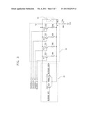
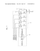
[0021] FIG. 3 is a circuit diagram of a precharge voltage supplying circuit according to another embodiment of the present disclosure.
[0022] Referring to FIG. 3, the precharge voltage supplying circuit includes a first switch unit 50, a bleeder resistance unit 52 and a second switch unit 54 which connects node E to node F.
[0023] The first switch unit 50 includes an NMOS transistor N50 and a PMOS transistor P50 which are connected between node E and node F and are turned on in response to enable signals BLEEDER OFF and BLEEDER OFFB. Here, it is desirable to design the NMOS transistor N50 and the PMOS transistor P50 to have a large size.
[0024] The bleeder resistance unit 52 includes NMOS transistors N51 to N54 which are connected between node E to which the internal voltage Vp is applied and node F to which the precharge voltage VBLP is supplied and operate in response to the control signals BLEEDER_XL, BLEEDER_L, BLEEDER_M and BLEEDER_S, respectively, and resistance elements 10K, 20K, 40K and 80K which are in series connected with the NMOS transistors N51 to N54, respectively.
[0025] Operation of the precharge voltage supplying circuit of FIG. 3 will be described below in detail.
[0026] The bleeder resistance unit 52 operates in response to the enable signals BLEEDER OFF and BLEEDER OFFB. First, in a case that the enable signals BLEEDER OFF and BLEEDER OFFB are in high and low levels, respectively, the NMOS transistor N50 and the PMOS transistor P50 are turned on. Since the sizes of the NMOS transistor N50 and the PMOS transistor P50 are large, the voltage drop between node E and node F through the turn-on resistance of the NMOS transistor N50 and the PMOS transistor P50 is not so large. Thus, the second bit line precharge voltage VBLP, having a level which is almost the same as the internal voltage Vp, is output through node F. At this time, there is almost no voltage drop through the bleeder resistance unit 52 which includes the NMOS transistors N51 to N54 and the resistance elements 10K, 20K, 40K and 80K. Also, if the second switch unit 54 is turned on so that node E is connected to node F, operation of the bleeder resistance unit 52 is bypassed, and the second bit line precharge voltage VBLP, having a level which is almost the same as the internal voltage Vp, is output through node F.
[0027] Meanwhile, in a case that the enable signal BLEEDER OFF is in a low level, the NMOS transistor N50 and the PMOS transistor P50 are turned off. Thus, a voltage drop of the internal voltage Vp occurs through the bleeder resistance unit 52 so that the voltage-dropped signal is outputted as the precharge voltage VBLP through node F. At this time, since the bleeder resistance unit 52 includes the NMOS transistors N51 to N54 and the resistance elements 10K, 20K, 40K and 80K, the precharge voltage VBLP is adjustable in various levels according to a PVT fluctuation and the range in the fluctuation is not so large. At this time, the level of the precharge voltage VBLP is adjustable according to the control signals BLEEDER_XL, BLEEDER_L, BLEEDER_M and BLEEDER_S. For example, in a case that the control signals BLEEDER_L, BLEEDER_M and BLEEDER_S are in a low level and only the control signal BLEEDER_XL is in a high level, the part which outputs the precharge voltage VBLP through node F with the voltage drop of the internal voltage Vp becomes the NMOS transistor N54 which is turned on and the resistance element 80K. It is possible to generate the precharge voltage which has various voltage levels based on the selective activation of the control signals BLEEDER_XL, BLEEDER_L, BLEEDER_M and BLEEDER_S.
[0028] Although various examples and exemplary embodiments of a precharge voltage supplying circuit that can be used to generate a bit line precharge voltage for performing a bit line precharge operation are described in the present disclosure, it can also be widely used in various other devices which need generation of a voltage, a level of which is adjustable according to a PVT characteristic change, and a range in change of which is not so large.
[0029] Although examples and exemplary embodiments of the invention have been disclosed for illustrative purposes, those skilled in the art will appreciate that various modifications, additions and substitutions are possible, without departing from the scope and spirit of the disclosure and the accompanying claims. For example, elements and/or features of different examples and illustrative embodiments may be combined with each other and/or substituted for each other within the scope of this disclosure and appended claims.
User Contributions:
Comment about this patent or add new information about this topic:
Images included with this patent application:
 |  |
 |  |
 |  |
 |
| New patent applications in this class: | |
| Date | Title |
|---|---|
| 2019-05-16 | Semiconductor apparatus |
| 2017-08-17 | Selectors on interface die for memory device |
| 2016-06-23 | Semiconductor memory device and method of testing the same |
| 2016-05-19 | Semiconductor device and operating method thereof |
| 2016-05-12 | Signal transition analysis of a circuit |
| New patent applications from these inventors: | |
| Date | Title |
|---|---|
| 2022-03-31 | Power control circuit, semiconductor apparatus including the same and power control method of semiconductor apparatus |
| 2018-12-27 | Address control circuit and semiconductor device including the same |
| 2013-03-28 | Refresh method and apparatus for a semiconductor memory device |
| 2012-01-12 | Semiconductor memory device to reduce off-current in standby mode |
| 2011-10-06 | Semiconductor memory apparatus |
| Top Inventors for class "Static information storage and retrieval" | |
| Rank | Inventor's name |
|---|---|
| 1 | Frankie F. Roohparvar |
| 2 | Vishal Sarin |
| 3 | Roy E. Scheuerlein |
| 4 | Yan Li |
| 5 | Yiran Chen |