Patent application title: ELECTROPHORISES DISPLAY UNIT AND ITS PRODUCTION METHOD
Inventors:
Po-Wen Hsiao (Hsinchu, TW)
Tzu-Ming Wang (Hsinchu, TW)
Kai-Cheng Chuang (Hsinchu, TW)
Gwo-Feng Hwang (Hsinchu, TW)
IPC8 Class: AH01J100FI
USPC Class:
313235
Class name: Electric lamp and discharge devices imperfect electrical contact between electrodes
Publication date: 2011-06-23
Patent application number: 20110148277
Abstract:
An electrophorises display unit includes a substrate, a first electrode,
a first insulation layer, a second electrode and a second insulation
layer. The first electrode is disposed on the substrate. The first
insulation layer is disposed on the first electrode. The second electrode
is disposed on the first insulation layer. The second insulation layer is
disposed on the second electrode. Wherein, the second insulation layer
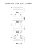
has an opening for appearing a part of the second electrode.Claims:
1. An electrophorises display unit comprising: a substrate; a first
electrode disposed on the substrate; a first insulation layer disposed on
the first electrode; at least a second electrode disposed on the first
insulation layer; and a second insulation layer disposed on the second
electrode, wherein the second insulation layer has an opening for
appearing a part of the second electrode.
2. The electrophorises display unit of claim 1, further comprising a third electrode disposed on the second insulation layer.
3. The electrophorises display unit of claim 1, wherein the second electrode is disposed on a part of the first insulation layer.
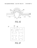
4. The electrophorises display unit of claim 1, wherein a part of the second electrode is covered by the second insulation layer.
5. The electrophorises display unit of claim 1, wherein the opening an electrophoretic liquid is filled from.
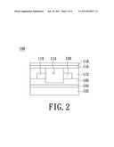
6. A production method for an electrophorises display unit comprising: providing a substrate, the substrate having a first electrode and a first insulation layer; disposing at least a second electrode on the first insulation layer; disposing a second insulation layer on the second electrode; and forming an opening on the second insulation layer for appearing a part of the second electrode.
7. The production method for the electrophorises display unit of claim 6, further comprising disposing a third electrode on the second insulation layer.
8. The production method for the electrophorises display unit of claim 6, wherein the second electrode is disposed on a part of the first insulation layer.
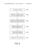
9. The production method for the electrophorises display unit of claim 6, wherein the second insulation layer encloses a part of the second electrode.
10. The production method for the electrophorises display unit of claim 6, wherein an electrophoretic liquid is filled from the opening.
Description:
CROSS-REFERENCE TO RELATED APPLICATIONS
[0001] This application is based upon and claims the benefit of priority from the prior Taiwanese Patent Application No. 098144283, filed Dec. 22, 2009, the entire contents of which are incorporated herein by reference.
BACKGROUND
[0002] 1. Field of the Invention
[0003] The present invention relates to a display. More particularly, the present invention relates to an electrophorises display unit and its production method.
[0004] 2. Description of the Related Art
[0005] Most of conventional electrophorises displays utilize voltage difference between top and bottom electrodes for driving particles within an electrophoretic layer to generate grayscale change. Along with the progress of electrophorises display techniques, the requirement for grayscale change and response time grows higher and higher. Although the display performance can be increased by means of improving display materials or driving method, but the efficiency still has room to be improved. In color electrophorises displays, the display panel includes at least a pixel with two kinds of particles, and a plurality of control electrodes between neighboring pixels. By means of applying a control voltage to an additional control electrode, for controlling distribution of different particles so as to change display images.
BRIEF SUMMARY
[0006] The present invention provides an electrophorises display unit, which disposes a side electrode between top and bottom electrodes, making the electrophorises display unit display more grayscale change.
[0007] The present invention also provides a method for producing an electrophorises display unit, by means of roll to roll procedure to form an opening for appearing the side electrode, therefore, can greatly shorten production time, decrease photo-mask and further decrease production cost and improve productivity.
[0008] The present invention provides an electrophorises display unit, which includes a substrate, a first electrode, a first insulation layer, a second electrode and a second insulation layer. The first electrode is disposed on the substrate. The first insulation layer is disposed on the first electrode. The second electrode is disposed on the first insulation layer. The second insulation layer is disposed on the second electrode. Wherein, the second insulation layer has an opening for appearing a part of the second electrode.
[0009] In an embodiment of the present invention, the electrophorises display unit further includes a third electrode disposed on the second insulation layer.
[0010] In an embodiment of the present invention, the second electrode is disposed on a part of the first insulation layer.
[0011] In an embodiment of the present invention, the second insulation layer encloses a part of the second electrode.
[0012] In an embodiment of the present invention, an electrophoretic liquid is filled from the opening.
[0013] A production method for an electrophorises display unit includes the following steps. First, providing a substrate having a first electrode and a first insulation layer. Next, disposing a second electrode on the first insulation layer. Next, disposing a second insulation layer on the second electrode. Next, forming an opening on the second insulation layer for appearing a part of the second electrode.
[0014] In the present invention introduces side electrode into the microcup of the display layer by means of roll to roll procedure, for controlling the motivation of the electrophoresis particles by voltage changes between the original two electrodes and the third electrode. Therefore, not only increases the response time by means of efficiently reducing moving distance of the particles and increases grayscale changes, but also greatly shortens the production time by means of utilizing roll to roll procedure, decreases photo-mask and further decreases production cost and improves productivity.
BRIEF DESCRIPTION OF THE DRAWINGS
[0015] These and other features and advantages of the various embodiments disclosed herein will be better understood with respect to the following description and drawings, in which like numbers refer to like parts throughout, and in which:
[0016] FIGS. 1A to 1F are schematic views shown producing procedures of an embodiment of the present invention
[0017] FIG. 2 is a side, cross sectional view of an embodiment of the electrophorises display of the present invention.
[0018] FIG. 3 is a flow chart of a production method of the electrophorises display according to an embodiment of the present invention.
DETAILED DESCRIPTION
[0019] FIGS. 1A to 1D are schematic views shown producing procedures of an embodiment of the present invention. Referring to FIG. 1A, in the procedure of forming an electrophorises display unit 100, a substrate 102 is provided, wherein the substrate 102 is of a flexible substrate.
[0020] In this embodiment, a first electrode 104 is disposed on the substrate 102, and for example, covers the entire substrate 102. The electrophorises display unit 100 is for providing a first control voltage to the first electrode 104.
[0021] Then, a first insulation layer 106 is formed on the first electrode 104, and for example, covers the entire first electrode 104. Thereafter, as shown in FIG. 1B, two second electrodes 108 and 110 are disposed on the first insulation layer 106. The electrophorises display unit 100 is for providing the second control voltages to the second electrodes 108 and 110. In this embodiment, two second electrodes 108 and 110 are taken as example but the amount of the second electrodes is not limited.
[0022] In a preferred embodiment of the present invention, the second electrode 108 and 110 are respectively disposed on one part of the first insulation layer 106. The second electrodes 108 and 110 are, for example, transparent electrodes, and may be selected from Indium Tin Oxide (ITO), Indium Zinc Oxide (IZO), ZnO, InGaZnO (IGZO), Al or Cu.
[0023] In a preferred embodiment of the present invention, the second electrodes 108 and 110 may be, for example, formed by inkjet printing or optical lithography method, but is not limited.
[0024] Referring to FIG. 1C, a second insulation layer 112 is disposed on the second electrodes 108 and 110, and on the first insulation layer 106 at a portion uncovered by the second electrodes 108 and 110. The second insulation layer 112 encloses the second electrodes 108 and 110, and covers the first insulation layer 106 at the portion uncovered by the second electrodes 108 and 110.
[0025] In a preferred embodiment of the present invention, the second insulation layer 112 may be, for example, of opacity insulation wall, and may be, for example, composed of resins polymerized by heat or by radiation. The second insulation layer 112 may be, for example, of the same material as the first insulation layer 106, but is not limited.
[0026] Referring to FIG. 1D, an opening 114 is formed on the second insulation layer 112 between the second electrodes 108 and 110 by roll to roll procedure. A depth of the opening 114 is, fox example, equal to or greater than a depth of the second insulation layer 112. In addition, a width of the opening 114 may be a distance between the second electrodes 108 and 110, for appearing a part of the second electrodes 108 and 110 out of the opening 114.
[0027] In a preferred embodiment of the present invention, the opening 114 is formed by getting rid of unnecessary part of the second insulation layer 112 by means of roll to roll procedure.
[0028] Referring to FIG. 1E, the roll to roll procedure is executed by a pressure wheel 122 and rolling wheels 124 and 126. In this embodiment, the electrophorises display unit 100 displayed in FIG. 1D is rolled between the pressure wheel 122 and the rolling wheels 124 and 126. Then, take advantage of saw tooth of the pressure wheel 122, forming the opening 114 on the second insulation layer 112 of the electrophorises display unit 100, thereby obtaining the electrophorises display unit 100 of FIG. 1D.
[0029] FIG. 1F is a top view of FIG. 1D. If FIG. 1F is cut along line A-A' and viewed from one side, FIG. 1D is obtained. Referring to FIG. 1F, the electrophorises display 10 is composed by a plurality of electrophorises display units 100. The electrophorises display unit 100 may be of inverted H-shaped and the opening 114 is formed at the cutout of the H-shape.
[0030] In a preferred embodiment of the present invention, it is obvious for one skilled in the art to form the opening 114 by yellow light process technology, but is not limited. FIG. 2 is a side, cross sectional view of an embodiment of the electrophorises display of the present invention. In this embodiment, after the opening 114 is formed, the electrophorises display unit 100 may be considered as a microcup structure. Therefore, the electrophoretic liquid with the electrophoresis particles may be filled from the opening 114 and a sealing layer 116 may be disposed on the second insulation layer 112 to prevent the electrophoretic liquid from leakage.
[0031] Then, a third electrode 118 is disposed on the sealing layer 116 and the electrophorises display unit 100 will provide a third control voltage to the third electrode 118.
[0032] In a preferred embodiment of the present invention, the first control voltage and the second control voltage have a voltage difference. The first control voltage and the third control voltage have a voltage difference, and the second control voltage and the third control voltage have a voltage difference.
[0033] FIG. 3 is a flow chart of a production method of the electrophorises display according to an embodiment of the present invention. Referring to FIGS. 1A to 1D and FIG. 3, in this embodiment, a substrate 102 is provided at first (step S302). Next, a first electrode 104 is formed on the substrate 102 (Step 304). Next, a first insulation layer 106 is formed on the first electrode 104. Wherein, it is obvious for one skilled in the art, the first electrode 104 covers a top surface of the entire substrate 102. The first insulation layer 160 covers a top surface of the entire first electrode 104.
[0034] After step 304, the second electrodes 108 and 110 are formed on a part of the first insulation layer 106 (step S306). The method of forming the second electrodes 108 and 110 may be, for example, firstly forming a second electrode layer on a top surface of the first insulation layer 106 and then acquiring the second electrodes 108 and 110 by pattern procedure.
[0035] After the second electrodes 108 and 110 are acquired, a second insulation layer 112 is formed on the second electrodes 108 and 110 and on the first insulation layer 106 at the portion uncovered by the second electrodes 108 and 110 (Step S306). The second insulation layer 112 respectively encloses the second electrodes 108 and 110. That is, the second insulation layer 112 respectively contacts with the three surfaces of each of the second electrodes 108 and 110.
[0036] Next, the opening 114 is formed on the second insulation layer 112 by roll to roll procedure for respectively appearing one surface of the second electrodes 108 and 110 (Step S308). The width of the opening 114 is equal to the distance between the second electrodes 108 and 110, and the height of the opening 114 is at least equal to a distance between the top surface of the second insulation layer 112 and the top surface of the first insulation layer 106. In this embodiment, in the process of forming the opening 114, the height of the opening 114 is greater than the distance between the top surface of the second insulation layer 112 and the top surface of the first insulation layer 106.
[0037] Next, the electrophoretic liquid with the electrophoresis particles is filled in the electrophorises display unit from the opening 114 (Step S310), and the sealing layer 116 is formed on the other parts of the second insulation layer 112. Finally, the third electrode is formed 118 on the sealing layer 116 (Step S312). In the embodiment, the sealing layer 116 is disposed on a top surface of the other parts of the second insulation layer 112 and seals the opening 114.
[0038] In the present invention, the electrophorises display and its production method, introduces side electrode into the microcup of the display layer by means of roll to roll procedure, for controlling the motivation of the electrophoresis particles by voltage changes between the original two electrodes and the third electrode. Therefore, not only increases the response time by means of efficiently reducing moving distance of the particles and increases grayscale changes, but also greatly shortens the production time by means of utilizing roll to roll procedure, decreases photo-mask and further decreases production cost and improves productivity.
[0039] The above description is given by way of example, and not limitation. Given the above disclosure, one skilled in the art could devise variations that are within the scope and spirit of the invention disclosed herein, including configurations ways of the recessed portions and materials and/or designs of the attaching structures. Further, the various features of the embodiments disclosed herein can be used alone, or in varying combinations with each other and are not intended to be limited to the specific combination described herein. Thus, the scope of the claims is not to be limited by the illustrated embodiments.
User Contributions:
Comment about this patent or add new information about this topic:
| People who visited this patent also read: | |
| Patent application number | Title |
|---|---|
| 20140182347 | ULTRASONIC EXTRUSION APPARATUS FOR METAL MATERIAL |
| 20140182346 | ROLL-HOLDER CARTRIDGE FOR A ROLLING MILL |
| 20140182345 | METHOD AND PLANT FOR PRODUCING METAL ROLLED PRODUCTS |
| 20140182344 | LOCKING APPARATUS FOR PANELS OF COMPUTER DEVICE |
| 20140182343 | ELECTRICAL LOCKING DEVICE WITH FAIL-SAFE EMERGENCY RELEASE |
Images included with this patent application:
 |  |
 |  |
| New patent applications in this class: | |
| Date | Title |
|---|---|
| 2010-12-30 | Electron emitting element and method for producing electron emitting element |
| 2010-06-03 | Field emission device |
| 2009-11-19 | Electron emitter and image display apparatus |
| 2009-11-19 | Electron-emitting device and image display apparatus |
| 2009-10-15 | Electron emission device and display device using the same |
| New patent applications from these inventors: | |
| Date | Title |
|---|---|
| 2014-12-18 | Display panel and manufacturing method thereof |
| 2013-05-09 | Sub-pixel structure and pixel structure of color electrophoretic display |
| 2013-03-28 | Electronic device |
| 2013-03-07 | Electro-phoretic display device and fabricating method thereof |
| Top Inventors for class "Electric lamp and discharge devices" | |
| Rank | Inventor's name |
|---|---|
| 1 | Satoshi Seo |
| 2 | Shou-Shan Fan |
| 3 | Nobuharu Ohsawa |
| 4 | Liang Liu |
| 5 | Peng Liu |