Patent application title: ULTRAVIOLET-ERASABLE NONVOLATILE SEMICONDUCTOR DEVICE
Inventors:
Tetsuo Someya (Chiba-Shi, Chiba, JP)
IPC8 Class: AH01L27115FI
USPC Class:
257431
Class name: Responsive to non-electrical signal (e.g., chemical, stress, light, or magnetic field sensors) electromagnetic or particle radiation light
Publication date: 2016-01-07
Patent application number: 20160005744
Abstract:
In order to provide an ultraviolet-erasable nonvolatile semiconductor
device that has a high water resistance and is capable of erasing data by
ultraviolet rays, a protective film includes a silicon nitride film (12)
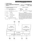
and a silicon oxynitride film (13). The silicon nitride film (12) and the
silicon oxynitride film (13) cooperate to prevent moisture from
penetrating into the ultraviolet-erasable nonvolatile semiconductor
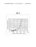
device. The silicon nitride film 12 has such a thickness with which a
time for erasing data in a nonvolatile semiconductor storage element (17)
through irradiation of the ultraviolet rays is not increased.Claims:
1. An ultraviolet-erasable nonvolatile semiconductor device, comprising:
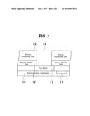
a semiconductor substrate; an ultraviolet-erasable nonvolatile
semiconductor storage element formed in a surface of the semiconductor
substrate; a top metal formed on the semiconductor substrate; and a
protective film formed on the ultraviolet-erasable nonvolatile
semiconductor storage element and the top metal, the protective film
comprising a silicon nitride film and a silicon oxynitride film laminated
thereon.
2. An ultraviolet-erasable nonvolatile semiconductor device according to claim 1, wherein the silicon nitride film has a thickness of 1,000 Å or more and 2,000 Å or less.
3. An ultraviolet-erasable nonvolatile semiconductor device according to claim 1, wherein the silicon oxynitride film has a refractive index of from 1.65 to 1.85.
4. An ultraviolet-erasable nonvolatile semiconductor device according to claim 1, further comprising a TEOS film formed between the silicon nitride film and the silicon oxynitride film.
Description:
TECHNICAL FIELD
[0001] The present invention relates to an ultraviolet-erasable nonvolatile semiconductor device.
BACKGROUND ART
[0002] Erosion by moisture has been a concern in a semiconductor device represented by a semiconductor integrated circuit. In order to cope with this, as disclosed in Patent Literature 1, a nitride film having an excellent water resistance is formed on a surface of the semiconductor device so that moisture is prevented from penetrating into the semiconductor device, to thereby enhance a water resistance of the semiconductor device.
CITATION LIST
Patent Literature
[0003] [PTL 1] JP 2006-344956 A
SUMMARY OF INVENTION
Technical Problem
[0004] However, when the technology disclosed in Patent Literature 1 is applied to an ultraviolet-erasable nonvolatile semiconductor device capable of erasing data by ultraviolet rays, due to the presence of the nitride film, the water resistance of the semiconductor device is enhanced but the ultraviolet rays are difficult to transmit therethrough, and hence the data cannot be erased by the ultraviolet rays or a large amount of time is required to erase the data. Thus, a structure has been demand that has a high water resistance and is suitable for an ultraviolet-erasable nonvolatile semiconductor device capable of erasing data by ultraviolet rays.
[0005] The present invention has been made in view of the problems described above, and provides an ultraviolet-erasable nonvolatile semiconductor device that has a high water resistance and is capable of erasing data by ultraviolet rays.
Solution to Problem
[0006] In order to solve the problems described above, according to one embodiment of the present invention, there is provided an ultraviolet-erasable nonvolatile semiconductor device, including: a semiconductor substrate; a nonvolatile semiconductor storage element formed in the semiconductor substrate; a top metal formed on the semiconductor substrate; and a protective film formed on the top metal. The protective film includes a silicon nitride film and a silicon oxynitride film. The silicon nitride film and the silicon oxynitride film cooperate to prevent moisture from penetrating into the ultraviolet-erasable nonvolatile semiconductor device. The silicon nitride film has such a thickness with which it is possible to shorten a time for erasing data in the nonvolatile semiconductor storage element through irradiation of ultraviolet rays.
Advantageous Effects of Invention
[0007] The ultraviolet-erasable nonvolatile semiconductor device according to the one embodiment of the present invention has the high water resistance and is capable of erasing the data by the ultraviolet rays.
BRIEF DESCRIPTION OF DRAWINGS
[0008] FIG. 1 is a sectional view of an ultraviolet-erasable nonvolatile semiconductor device.
[0009] FIG. 2 is a sectional view of an ultraviolet-erasable nonvolatile semiconductor device.
[0010] FIG. 3 is a graph for showing a relationship between a thickness of a silicon nitride film and a time for erasing data in an ultraviolet-erasable nonvolatile semiconductor storage element.
DESCRIPTION OF EMBODIMENTS
[0011] In the following, embodiments of the present invention are described with reference to the drawings.
[0012] An ultraviolet-erasable nonvolatile semiconductor device is now described. FIG. 1 is a sectional view of the ultraviolet-erasable nonvolatile semiconductor device. FIG. 3 is a graph for showing a relationship between a thickness of a silicon nitride film and a time for erasing data in an ultraviolet-erasable nonvolatile semiconductor storage element.
[0013] The ultraviolet-erasable nonvolatile semiconductor device includes a semiconductor substrate 10, a nonvolatile semiconductor storage element 17 formed in the semiconductor substrate 10, a top metal 11 formed on the semiconductor substrate 10, and a protective film formed on the top metal 11. Further, the ultraviolet-erasable nonvolatile semiconductor device includes, in part thereof, a pad opening portion 14 obtained by removing the protective film formed on the top metal 11. In this case, the protective film includes two layers of a silicon nitride film 12 and a silicon oxynitride film 13.
[0014] Part of the top metal 11 is exposed from the pad opening portion 14, and necessary signal transmission is performed therewith. The silicon nitride film 12 and the silicon oxynitride film 13 cooperate to prevent moisture from penetrating into the ultraviolet-erasable nonvolatile semiconductor device. As a thickness of the silicon nitride film 12 is increased, ultraviolet rays are more difficult to transmit therethrough, and hence such a thickness is selected with which it is possible to shorten the time for erasing data in the nonvolatile semiconductor storage element 17 through irradiation of the ultraviolet rays.
[0015] Through a publicly-known semiconductor manufacturing process, the nonvolatile semiconductor storage element 17 such as an erasable programmable read only memory (EPROM) is formed in the semiconductor substrate 10. After that, an inter-layer insulating film (not shown) and the like are laminated on the resultant, and then the top metal 11 is laminated thereon. After that, as the protective film, the silicon nitride film 12 and then the silicon oxynitride film 13 are laminated thereon. After that, the pad opening portion 14 is formed in part of the protective film formed on the top metal 11.
[0016] In this case, the silicon nitride film 12 is formed so as to have a thickness of about 1,000 Å or more in order to ensure the water resistance. Moreover, as shown in FIG. 3, when the thickness of the silicon nitride film 12 exceeds about 2,000 Å, the time for erasing data in the ultraviolet-erasable nonvolatile semiconductor storage element is precipitously increased. Thus, it is required that the thickness of the silicon nitride film 12 be set to be about 2,000 Å or less so that the time for erasing data is not unnecessarily increased. With this, the data in the nonvolatile semiconductor storage element 17 can be erased by the ultraviolet rays even in the manufacturing process.
[0017] Moreover, the silicon oxynitride film 13 is formed so as to have a refractive index of from 1.65 to 1.85 and a thickness of about 7,000 Å or more, and hence the water resistance can be enhanced. Note that, the silicon oxynitride film 13 does not inhibit the entrance of the ultraviolet rays.
[0018] With the configuration described above, the ultraviolet-erasable nonvolatile semiconductor device can have the high water resistance and erase the data by the ultraviolet rays within a period of time that allows the mass production.
[0019] Note that, in FIG. 1, the silicon oxynitride film 13 is laminated on the silicon nitride film 12. Although not illustrated, the silicon nitride film 12 may be laminated on the silicon oxynitride film 13.
[0020] Moreover, as illustrated in FIG. 2, a TEOS film 15 may be added as the protective film between the silicon nitride film and the silicon oxynitride film.
REFERENCE SIGNS LIST
[0021] 10 semiconductor substrate
[0022] 11 top metal
[0023] 12 silicon nitride film
[0024] 13 silicon oxynitride film
[0025] 14 pad opening portion
[0026] 15 TEOS film
[0027] 17 nonvolatile semiconductor storage element
User Contributions:
Comment about this patent or add new information about this topic:
Images included with this patent application:
 |  |
 |  |
| Similar patent applications: | |
| Date | Title |
|---|---|
| 2015-04-30 | Isolation device |
| 2016-04-14 | Non-volatile memory |
| 2011-05-12 | Stable light source |
| 2012-05-31 | Tileable sensor array |
| 2013-06-27 | Photovoltaic device |
| New patent applications in this class: | |
| Date | Title |
|---|---|
| 2022-05-05 | Solid-state image pickup apparatus and manufacturing method therefor, and electronic equipment |
| 2019-05-16 | Image sensor |
| 2016-04-14 | Optical semiconductor device including blackened tarnishable bond wires and related methods |
| 2015-12-31 | Light receiving device including transparent electrode and method of manufacturing light receiving device |
| 2015-05-21 | Image sensor package structure and method |
| Top Inventors for class "Active solid-state devices (e.g., transistors, solid-state diodes)" | |
| Rank | Inventor's name |
|---|---|
| 1 | Shunpei Yamazaki |
| 2 | Shunpei Yamazaki |
| 3 | Kangguo Cheng |
| 4 | Huilong Zhu |
| 5 | Chen-Hua Yu |