Patent application title: METHOD OF FORMING AN INTEGRATED INDUCTOR BY DRY ETCHING AND METAL FILLING
Inventors:
Pengfei Wang (Shanghai, CN)
Pengfei Wang (Shanghai, CN)
Qingqing Sun (Shanghai, CN)
Qingqing Sun (Shanghai, CN)
Wei Zhang (Shanghai, CN)
Wei Zhang (Shanghai, CN)
Assignees:
FUDAN UNIVERSITY
IPC8 Class: AH01L2166FI
USPC Class:
438 17
Class name: Semiconductor device manufacturing: process with measuring or testing electrical characteristic sensed
Publication date: 2014-12-25
Patent application number: 20140377892
Abstract:
The present invention discloses an inductive element formed by through
silicon via interconnections. The inductive element formed by means of
the special through silicon via interconnection by using through silicon
via technology features advantages such as high inductance and density.
Moreover, the through silicon via interconnection integrated process
forming the inductive element is compatible with the ordinary through
silicon interconnection integrated process without any other steps, thus
making the process simple and steady. The inductive element using the
present invention is applicable to the through silicon via package
manufacturing of various chips, especially the package manufacturing of
power control chips and radio-frequency chips.Claims:
1. A process for creating an inductive element comprising: a) applying a
specific current between a first set of measurement nodes; b) forming an
electromagnetic field around a metal conductor; and c) creating an
inductive element between a second set of measurement nodes.
2. The process as in claim 1, wherein said step of creating an inductive element comprises providing at least one semiconductor.
3. The process as in claim 1, wherein said step of providing at least one semiconductor comprises: stacking and interconnecting a plurality of silicon wafers alternatively on a semiconductor substrate.
4. The process as in claim 3, wherein said step of providing at least one semiconductor comprises providing at least one monocrystalline silicon or monocrystalline silicon on an insulator.
5. The process as in claim 3, wherein said step of providing at least one semiconductor comprises providing at least one polycrystalline silicon or polycrystalline silicon on an insulator.
6. A process for creating an inductive loop comprising: a) connecting a first set of measurement nodes in a short circuit method; b) forming a closed loop around a metal conductor to form an inductive element; c) forming mutual inductance with said inductive element being formed by said metal conductor.
7. The process as in claim 6, wherein said step of forming an inductive element comprises providing at least one semiconductor.
8. The process as in claim 6, wherein said step of providing at least one semiconductor comprises: stacking and interconnecting a plurality of silicon wafers alternatively on a semiconductor substrate.
9. The process as in claim 8, wherein said step of providing at least one semiconductor comprises providing at least one monocrystalline silicon or monocrystalline silicon on an insulator.
10. The process as in claim 6, wherein said step of providing at least one semiconductor comprises providing at least one polycrystalline silicon or polycrystalline silicon on an insulator.
Description:
CROSS REFERENCE TO RELATED APPLICATIONS
[0001] This application is a divisional application of Ser. No. 13/392,208 filed on Feb. 24, 2012, which is the National Stage of PCT/CN2011/000871 filed on May 19, 2011, which claims priority under 35 U.S.C. '119 of People's Republic of China Application No. 201010179375.0 filed on May 20, 2010, the disclosure of all of these applications are incorporated by reference. The international application under PCT article 21(2) was not published in English.
TECHNICAL FIELD
[0002] The present invention belongs to the technical field of highly integrated packaging technology, and relates to an integrated packaging technology using through silicon vias, and especially to an inductive loop formed by through silicon vias.
DESCRIPTION OF THE RELATED ART
[0003] Currently, three-dimensional packaging technology has been developed such as the through silicon via (TSV) interconnection packaging technology at the wafer level from the stacked die packaging or package on package at chip level.
[0004] Through silicon via is such a technology that, through making vertical vias between the silicon wafers and forming interconnection micro-joints on the front and back of the silicon wafers, several silicon wafers can be stacked directly without external lead wire interconnections. Through silicon via technology can be classified into two kinds, via first and via last. Via first is a technology where interconnection via are formed on the silicon wafers before finishing manufacturing the integrated circuit, wherein the through silicon via interconnection can be formed both at the primary steps of chip manufacturing and before BEOL (Back-end of Line). While via last is a technology where through silicon vias are interconnected after BEOL or finishing manufacturing the integrated circuit. The filling materials in the through silicon via include an insulation layer and a metal layer or highly-doped polycrystalline silicon used for electricity conduction. In order to decrease interconnection resistance and improve the working frequency of the chip, in the through silicon via three-dimensional package with multiple sensing systems, it is more preferable to use copper as the through silicon via interconnection metal. Different from the previous IC package bonding or the stacking technology using bumps, through silicon via interconnection technology can maximize the stacking density and minimize the external dimensions of the chip in three-dimensional direction, and improve the speed and performance of low power consumption greatly.
[0005] The integrated circuit made of silicon has a wide application prospect in the radio-frequency circuit field. The radio-frequency inductive element has an indispensable effect on the requirements of portable wireless communication equipment in low power voltage, power consumption, power dissipation, distortion and high working frequency, etc. However, seen from the silicon integrated circuit process of current standards, the inductive element is very difficult to be integrated or has very low inductance if integrated.
BRIEF SUMMARY OF THE INVENTION
[0006] With respect to the problems above, the present invention aims at providing an inductive element used in silicon integrated circuits, wherein the inductive element is easy to be integrated in chips and has a high inductance.
[0007] To achieve the above purpose, the present invention provides an inductive loop used to form through silicon via interconnections, comprising:
[0008] A semiconductor substrate;
[0009] Two or more (more than two) silicon wafers with finished through silicon via structures;
[0010] Interconnection joints formed on the front and back of the silicon wafers;
[0011] An inductive element formed on the semiconductor substrate, which is used to stack and interconnect the silicon wafers.
[0012] The semiconductor substrate is made of monocrystalline or polycrystalline silicon or silicon on insulators (SOI). The through silicon via structures of the silicon wafers comprises at least a conductive layer and an insulation layer isolating the conductive layer from the through silicon via surface. The insulation layer is made of silicon dioxide, or silicon nitride or the insulation substance of their combination. The conductive layer is made of aluminium, or copper or doped polycrystalline silicon.
BRIEF DESCRIPTION OF THE SEVERAL VIEWS OF THE DRAWINGS
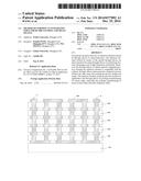
[0013] FIG. 1 is the cross sectional view of an inductive element formed by interconnecting the through silicon vias by means of through silicon via technology of the present invention.
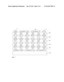
[0014] FIG. 2 is the top view of an embodiment integrating an inductive element with a analog or logic circuit of the present invention.
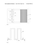
[0015] FIG. 3 is the schematic view when an inductive element works according to the present invention.
DETAILED DESCRIPTION OF THE INVENTION
[0016] An exemplary embodiment of the present invention is further detailed herein by referring to the drawings. The reference drawings are the schematic diagrams of the ideal embodiments of the present invention. The embodiments below are for description only rather than restricting the present invention.
[0017] Provide a semiconductor and several silicon wafers with through silicon vias and finished interconnection joints. In the embodiment, five silicon wafers with through silicon vias structure and finished interconnection joints are provided.
[0018] Next, stack and interconnect the five silicon wafers alternatively on the semiconductor substrate, as shown in FIG. 1, the semiconductor substrate 100 can be monocrystalline or polycrystalline silicon or silicon on insulators (SOI). 101, 102, 103, 104 and 105 are the five silicon wafers with through silicon vias and interconnection joints finished in the embodiment. 106 is the metal conductor after the through silicon via interconnection, wherein the metal conductor 106 comprises a conductive layer and an insulation layer isolating the conductive layer from the through silicon via surface. a and b are two measurement nodes introduced in the embodiment.
[0019] The inductive element provided by the present invention, which is used to form through silicon via interconnections, is compatible with simulation or logic circuits. FIG. 2 is the top view when integrating the inductive element provided by the embodiment of the present invention with a simulation or logic circuit. As shown in FIG. 2, 200 is a semiconductor substrate made of monocrystalline or polycrystalline silicon, wherein 201 is logic or simulation circuit, 203 is the interconnection metal conductor between measurement nodes a and b, which can be made of aluminium or copper, and 204 is the interconnection metal conductor between measurements c and d, which can be made of aluminium or copper.
[0020] FIG. 3 is the schematic diagram when the inductive element provided by the embodiment of the present invention, wherein 301 and 302 are the interconnection metal conductors between measurement nodes a, b and c, d respectively. Connecting the measurement nodes a, b, c and d in different schemes, inductive elements with different inductances can be made. Two connection schemes are provided in the embodiment.
[0021] Scheme 1: applying a specific current between measurement nodes c and d, the current flows through the metal conductor 302 and forms an electromagnetic field around the metal conductor 302, thus the metal conductor 301 between measurement nodes a and b is an inductive element.
[0022] Scheme 2: connect measurement nodes c and d in a short circuit method, and then the metal conductor 302 can form a closed loop to be an inductive element capable of forming mutual inductance with the inductive element formed by the metal conductor 301.
[0023] As described above, there are many significantly different embodiments without deviating from the spirit and scope of the present invention. It shall be understood that the present invention are not limited to the specific embodiments described in the Specification except those limited by the Claims herein.
Industrial Applicability
[0024] The inductive element formed by means of the special through silicon via interconnection by using through silicon via technology features advantages such as high inductance and density. Moreover, the through silicon via interconnection integrated process forming the inductive element is compatible with ordinary through silicon interconnection integrated process without any other steps, thus making the process simple and steady. The inductive element of the present invention is applicable to the through silicon via interconnection package manufacturing of various chips, especially the package manufacturing of power control chip and radio-frequency chip.
User Contributions:
Comment about this patent or add new information about this topic:
Images included with this patent application:
 |  |
 |
| Similar patent applications: | |
| Date | Title |
|---|---|
| 2014-12-04 | Methods of crystallising thin films |
| 2014-09-18 | Metric for recognizing correct library spectrum |
| 2014-12-11 | Electron beam-induced etching |
| 2014-09-18 | Interface for metal gate integration |
| 2014-10-02 | Sige sram butted contact resistance improvement |
| New patent applications in this class: | |
| Date | Title |
|---|---|
| 2016-06-30 | Manufacturing method of semiconductor device |
| 2016-05-19 | Probe pad with indentation |
| 2016-05-05 | Method for processing a substrate and a method of process screening for integrated circuits |
| 2016-04-21 | Method and apparatus for characterizing metal oxide reduction |
| 2016-03-31 | Solar cell manufacturing method |
| New patent applications from these inventors: | |
| Date | Title |
|---|---|
| 2022-07-14 | Distributed braking system in automobile, automobile, and control method therefor |
| 2022-07-14 | Brake system of vehicle, vehicle, and control method for brake system |
| 2022-03-31 | Graphics processor and acceleration method thereof |
| 2022-03-31 | Electric vehicle's drive system and method for controlling the same |
| Top Inventors for class "Semiconductor device manufacturing: process" | |
| Rank | Inventor's name |
|---|---|
| 1 | Shunpei Yamazaki |
| 2 | Shunpei Yamazaki |
| 3 | Kangguo Cheng |
| 4 | Chen-Hua Yu |
| 5 | Devendra K. Sadana |