Patent application title: CIRCUIT FOR ENHANCING ROBUSTNESS OF SUB-THRESHOLD SRAM MEMORY CELL
Inventors:
Na Bai (Jiangsu, CN)
Longxing Shi (Jiangsu, CN)
Longxing Shi (Jiangsu, CN)
Jun Yang (Jiangsu, CN)
Xinning Liu (Jiangsu, CN)
Jiafeng Zhu (Jiangsu, CN)
Yue Feng (Jiangsu, CN)
Cai Gong (Jiangsu, CN)
Fei Pan (Jiangsu, CN)
Hong Chang (Jiangsu, CN)
Yifeng Deng (Jiangsu, CN)
Yuan Chen (Jiangsu, CN)
Yingcheng Xia (Jiangsu, CN)
IPC8 Class: AG11C11419FI
USPC Class:
365156
Class name: Systems using particular element flip-flop (electrical) complementary
Publication date: 2014-12-25
Patent application number: 20140376305
Abstract:
The present invention discloses a circuit for improving process
robustness of sub-threshold SRAM memory cells, which serves as an
auxiliary circuit for a sub-threshold SRAM memory cell. The output of the
circuit is connected to the PMOS tube of the sub-threshold SRAM memory
cell and the substrate of a PMOS tube in the circuit. The circuit
comprises a detection circuit for threshold voltage of PMOS tube and a
differential input and single-ended output amplifier. The circuit changes
the substrate voltage of the PMOS tubes in the sub-threshold SRAM memory
cell and the substrate voltage of the PMOS tube in the circuit in a
self-adapting manner by detecting threshold voltage fluctuations of PMOS
tubes and NMOS tubes resulted from process fluctuations and thereby
regulate the threshold voltages of the PMOS tubes, so that the threshold
voltage of PMOS tubes matches the threshold voltage of NMOS tubes. The
circuit improves the noise margin of sub-threshold SRAM memory cells and
effectively improves the process robustness of sub-threshold SRAM memory
cells.Claims:
1. A circuit for improving process robustness of sub-threshold SRAM
memory cells, wherein, the circuit serves as an auxiliary circuit for a
sub-threshold SRAM memory cell, the output (Vbp) of the circuit is
connected to the PMOS tube of the sub-threshold SRAM memory cell and the
substrate of a PMOS tube in the circuit; the circuit comprises a
detection circuit for threshold voltage of PMOS tube and a differential
input and single-ended output amplifier, wherein: the detection circuit
for threshold voltage of PMOS tube comprises a first PMOS tube P1 and a
first NMOS tube N1; the source terminal of the first PMOS tube P1 is
connected to the supply voltage VDD, and the drain terminal and gate
terminal of the first PMOS tube P1 are connected with the drain terminal
and gate terminal of the first NMOS tube N1; the source terminal and
substrate of the first NMOS tube N1 are both connected to the power
ground VSS; the differential input and single-ended output amplifier
comprises a second PMOS tube P2, a third PMOS tube P3, a fourth PMOS tube
P4, a second NMOS tube N2, a third NMOS tube N3, a fourth NMOS tube N4,
and a fifth NMOS tube N5; the drain terminal and gate terminal of the
second PMOS tube P2 are connected together and then connected with the
gate terminal of the third PMOS tube P3 and the drain terminal of the
second NMOS tube N2, the source terminal of the second PMOS tube P2 is
connected with the source terminal of the third PMOS tube P3 and then
connected to the supply voltage VDD; the gate terminal of the second NMOS
tube N2 is connected with the gate terminal of the fourth NMOS tube N4
and then connected to the external bias voltage (Vbais), the source
terminal of the second NMOS tube N2 is connected with the source terminal
of the third NMOS tube N3 and the drain terminal of the fourth NMOS tube
N4, the source terminal of the fourth NMOS tube N4 is connected to the
power ground VSS, the gate terminal of the third NMOS tube N3 is
connected with the drain terminal and gate terminal of the first NMOS
tube N1 in the detection circuit for threshold voltage of PMOS tube, the
drain terminal of the third NMOS tube N3 is connected with the drain
terminal of the third PMOS tube P3, the gate terminal of the fourth PMOS
tube P4, and the gate terminal of the fifth NMOS tube N5, the source
terminal of the fourth PMOS tube P4 is connected to the supply voltage
VDD, and the gate terminal of the fifth NMOS tube N5 is connected to the
power ground VSS; the substrates of the second NMOS tube N2, third NMOS
tube N3, fourth NMOS tube N4, and fifth NMOS tube N5 are connected to the
power ground VSS, the drain terminal of the fourth PMOS tube P4 is
connected with the drain terminal of the fifth NMOS tube N5 and connected
with the substrates of the first PMOS tube P1, the second PMOS tube P2,
the third PMOS tube P3, and the fourth PMOS tube P4 to serve as the
output terminal (Vbp) of the present auxiliary circuit.Description:
FIELD OF THE INVENTION
[0001] The present invention relates to a circuit for improving process robustness of sub-threshold SRAM (Static Random Access Memory) memory cells, and belongs to the technical field of integrated circuit design.
BACKGROUND OF THE INVENTION
[0002] Sub-threshold design has been widely applied owing to its ultra-low energy consumption characteristic. However, as the system supply voltage enters into the sub-threshold region, the impact of process fluctuations on the threshold voltage of MOS tubes in memory cells becomes more severe. For SRAM memory circuits, process fluctuations may result in degraded performance and even faults of the memory cells. That phenomenon brings a new challenge to stability design of the entire system. Therefore, it is necessary to employ process fluctuation compensation measures to improve stability of SRAM memory cells.
[0003] In the sub-threshold region, the threshold voltage of MOS tube is in an exponential relationship with the driving power; therefore, the driving power of MOS tube can be changed effectively by changing the threshold voltage of sub-threshold MOS tube. Changing the substrate voltage of MOS tube is one of the most effective measures for changing the threshold voltage of MOS tube. However, owing to the fact that the substrate voltage of NMOS tube manufactured in a single well process is the power ground, changing the substrate voltage of PMOS tube is an effective approach to implement that method.
SUMMARY OF THE INVENTION
[0004] Object of the invention: the object of the present invention is to provide a circuit for improving process robustness of sub-threshold SRAM memory cells, in order to solve the problem that the threshold voltage of MOS tubes in the sub-threshold region is affected by process fluctuations and may result in degraded performance and even failures of SRAM memory cells. By detecting threshold voltage fluctuations of the PMOS tubes and NMOS tubes resulted from process fluctuations, the circuit changes the substrate voltage of the PMOS tubes in a sub-threshold memory cell and thereby regulates the threshold voltage thereof, so that the threshold voltage of the PMOS tubes in the sub-threshold memory cell matches the threshold voltage of the NMOS tubes; in that way, the noise margin of the memory cell is increased and the process robustness of the sub-threshold SRAM memory cell is effectively improved.
[0005] Technical solution: a circuit for improving process robustness of sub-threshold SRAM memory cells, which serves as an auxiliary circuit of a sub-threshold SRAM memory cell, with the output (Vbp) of the circuit being connected to the substrates of PMOS tubes in the sub-threshold SRAM memory cell; the circuit comprises a detection circuit for threshold voltage of PMOS tube and a differential input and single-ended output amplifier, wherein:
[0006] The detection circuit for threshold voltage of PMOS tube comprises a PMOS tube P1 and a NMOS tube N1, the source terminal of the PMOS tube P1 is connected to the supply voltage VDD, the drain terminal and gate terminal of the PMOS tube P1 are connected with the drain terminal and gate terminal of the NMOS tube N1 respectively, and the source terminal and substrate of the NMOS tube N1 are connected together and then connected to the power ground VSS;
[0007] The differential input and single-ended output amplifier comprises a second PMOS tube P2, a third PMOS tube P3, a fourth PMOS tube P4, a second NMOS tube N2, a third NMOS tube N3, a fourth NMOS tube N4, and a fifth NMOS tube N5; the drain terminal and gate terminal of the second PMOS tube P2 are connected together and then connected with the gate terminal of the third PMOS tube P3 and the drain terminal of the second NMOS tube N2, the source terminal of the second PMOS tube P2 is connected with the source terminal of the third PMOS tube P3 and then connected to the supply voltage VDD, the gate terminal of the second NMOS tube N2 is connected with the gate terminal of the fourth NMOS tube N4 and then connected to an external bias voltage (Vbais), the source terminal of the second NMOS tube N2 is connected with the source terminal of the third NMOS tube N3 and the drain terminal of the fourth NMOS tube N4, and the source terminal of the fourth NMOS tube N4 is connected to the power ground VSS; the gate terminal of the third NMOS tube N3 is connected with the drain terminal and gate terminal of the first NMOS tube N1 in the detection circuit for threshold voltage of PMOS tube, the drain terminal of the third NMOS tube N3 is connected with the drain terminal of the third PMOS tube P3, the gate terminal of the fourth PMOS tube P4 and the gate terminal of the fifth NMOS tube N5, the source terminal of the fourth PMOS tube P4 is connected to the supply voltage VDD, and the source terminal of the fifth NMOS tube N5 is connected to the power ground VSS;
[0008] The substrates of the second NMOS tube N2, third NMOS tube N3, fourth NMOS tube N4, and fifth NMOS tube N5 are connected to the power ground VSS, the drain terminal of the fourth PMOS tube P4 is connected with the drain terminal of the fifth NMOS tube N5 and connected with the substrates of the first PMOS tube P1, the second PMOS tube P2, the third PMOS tube P3, and the fourth PMOS tube P4 to serve as the output terminal (Vbp) of the auxiliary circuit.
[0009] Beneficial effects: compared with the prior art, the circuit for improving process robustness of sub-threshold SRAM memory cells in the present invention can be applied in a super-wide supply voltage range in the sub-threshold region in single-well process, and it can change the threshold voltage of the PMOS tubes by changing the substrate voltage of the PMOS tubes in a sub-threshold SRAM memory cell to make the threshold voltage of the PMOS tubes match the threshold voltage of the NMOS tubes in different processes, and thereby improve the noise margin of the sub-threshold SRAM memory cell and effectively improve the process robustness of the sub-threshold SRAM memory cell. The circuit can operate in a super-wide supply voltage range (0.2V˜0.7V) in the sub-threshold region.
BRIEF DESCRIPTION OF THE DRAWINGS
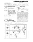
[0010] FIG. 1 is a structure diagram of the circuit provided in the present invention;
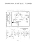
[0011] FIG. 2 is a structure diagram of the circuit in the present invention connected to a sub-threshold SRAM six-tube memory cell;
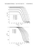
[0012] FIG. 3 is a gain diagram of the differential input and single-ended output amplifier used in the present invention;
[0013] FIG. 4 is a phase diagram of the differential input and single-ended output amplifier used in the present invention;
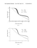
[0014] FIG. 5 shows the result of Monte Carlo analysis of reading noise margin for 500 times of a sub-threshold SRAM six-tube memory cell at 300 mV supply voltage;
[0015] FIG. 6 shows the result of Monte Carlo analysis of reading noise margin for 500 times of a sub-threshold SRAM six-tube memory cell that employs the design in the present invention at 300 mV supply voltage;
[0016] FIG. 7 shows the comparison of writing noise margin in the worst process corner in the sub-threshold region at different supply voltages between a sub-threshold SRAM six-tube memory cell that employs the circuit in the present invention and a sub-threshold SRAM six-tube memory cell that doesn't employs the circuit in the present invention;
[0017] FIG. 8 shows an example of the present invention applied in sub-threshold SRAM.
EMBODIMENTS
[0018] Hereunder the present invention will be further detailed in embodiments, with reference to the accompanying drawings. It should be understood that these embodiments are provided only for describing the present invention, and are not intended for limiting the scope of the present invention. Upon reading the present invention, those skilled in the art can make various equivalent modifications to the present invention without departing from the protection scope defined in the attached claims of the present application.
[0019] Please see FIG. 1. The circuit for improving process robustness of sub-threshold SRAM memory cells comprises a detection circuit for threshold voltage of PMOS tube. In addition, it requires an external bias voltage (Vbias).
[0020] The detection circuit for threshold voltage of PMOS tube comprises a first PMOS tube P1 and a first NMOS tube N1; the source terminal of the first PMOS tube P1 is connected to the supply voltage VDD, and the drain terminal and gate terminal of the first PMOS tube P1 are connected with the drain terminal and gate terminal of the first NMOS tube N1 respectively; the source terminal and substrate of the first NMOS tube N1 are connected together and then connected to the power ground VSS;
[0021] The differential input and single-ended output amplifier comprises a second PMOS tube P2, a third PMOS tube P3, a fourth PMOS tube P4, a second NMOS tube N2, a third NMOS tube N3, a fourth NMOS tube N4, and a fifth NMOS tube N5; the drain terminal and gate terminal of the second PMOS tube P2 are connected together and then connected with the gate terminal of the third PMOS tube P3 and the drain terminal of the second NMOS tube N2, the source terminal of the second PMOS tube P2 is connected with the source terminal of the third PMOS tube P3 and connected to the supply voltage VDD, the gate terminal of the second NMOS tube N2 is connected with the gate terminal of the fourth NMOS tube N4 and connected to an external bias voltage (Vbais), the source terminal of the second NMOS tube N2 is connected with the source terminal of the third NMOS tube N3 and the drain terminal of the fourth NMOS tube N4, and the source terminal of the fourth NMOS tube N4 is connected to the power ground VSS; the gate terminal of the third NMOS tube N3 is connected with the drain terminal and gate terminal of the first NMOS tube N1 in the detection circuit for threshold voltage of PMOS tube, the drain terminal of the third NMOS tube N3 is connected with the drain terminal of the third PMOS tube P3, the gate terminal of the fourth PMOS tube P4 and the gate terminal of the fifth NMOS tube N5, the source terminal of the fourth PMOS tube P4 is connected to the supply voltage VDD, and the source terminal of the fifth NMOS tube N5 is connected to the power ground VSS;
[0022] The substrates of the second NMOS tube N2, third NMOS tube N3, fourth NMOS tube N4, and fifth NMOS tube N5 are connected to the power ground VSS, the drain terminal of the fourth PMOS tube P4 is connected with the drain terminal of the fifth NMOS tube N5 and connected with the substrates of the first PMOS tube P1, the second PMOS tube P2, the third PMOS tube P3, and the fourth PMOS tube P4 to serve as the output terminal (Vbp) of the auxiliary circuit.
[0023] Please see FIG. 2. In the circuit model, the output terminal of the circuit for improving process robustness of sub-threshold SRAM memory cells is connected with the substrates of a fifth PMOS tube P5 and a sixth PMOS tube P6 in a sub-threshold SRAM six-tube memory cell, to verify that the present design can improve the process robustness of a sub-threshold SRAM memory cell.
[0024] The working principal of the circuit for improving process robustness of sub-threshold SRAM memory cells is as follows:
Detection Circuit for Threshold Voltage of PMOS Tube
[0025] As shown in FIG. 1, a first PMOS tube P1 and a first NMOS tube N1 constitute a detection circuit for threshold voltage of PMOS tube. The driving current of sub-threshold MOS tube (Isub) is expressed as follows:
I sub = μ C ox ( W L ) ( n - 1 ) V T 2 e V GS - V th nV T ( 1 ) ##EQU00001##
[0026] Wherein, μ is the mobility ratio of MOS tube, W/L is the width-length ratio of MOS tube, n is sub-threshold amplitude coefficient, VT is thermal voltage kT/q (approx. 26 mV at room temperature), and Vth is the threshold voltage of MOS tube.
[0027] The current in N1 and P1 is (i.sub.D,N1, i.sub.D,P1) respectively:
i D , N 1 = μ n C ox ( W L ) N 1 ( n - 1 ) V T 2 e V A - V thn nV T ( 2 ) i D , P 1 = μ p C ox ( W L ) P 1 ( n - 1 ) V T 2 e VDD - V A - V thp nV T ( 3 ) ##EQU00002##
[0028] Wherein, μn and μp are the mobility ratios of NMOS and PMOS respectively, n is sub-threshold amplitude coefficient, VT is thermal voltage kT/q, VDD is supply voltage, Vthn and Vthp are threshold voltage (absolute value) of NMOS and PMOS respectively.
[0029] It can be seen from the diagram: i.sub.D,N1=i.sub.D,P1, and suppose
( W L ) N 1 = ( W L ) P 1 , ##EQU00003##
then the level at point A (VA) is:
V A = 1 2 ( VDD + V thn - V thp + nV T ln u p u n ) ( 4 ) ##EQU00004##
[0030] It can be seen from the formula (4), VA is affected by the supply voltage VDD, Vthn, Vthp, μn, and μp. At a certain supply voltage, VDD is constant. The influence of μn and μp on VA is much lower than the influence of Vthn and Vthp in case of process fluctuations. Therefore,
nV T ln u p u n ##EQU00005##
is presumed as a fixed value here. Therefore, at a certain supply voltage, the level of VA is in a linear relationship with Vthn and Vthp.
[0031] In summary, if VA is set to a fixed value at a certain supply voltage in the sub-threshold region, Vthn and Vthp will be maintained in a fixed linear relationship. By setting the width-length ratio of PMOS and NMOS, the driving power of NMOS can be balanced with the driving power of PMOS in case of process fluctuations.
Differential Input and Single-Ended Output Amplifier
[0032] In the present design, the used differential amplifier is a two-stage amplifier. The first stage is a differential input and single-ended output amplifier, and the second stage is mainly designed to increase driving power of the present design and control the output oscillation amplitude of the amplifier within the range of 0 to VDD. FIG. 3 and FIG. 4 show gain diagram and phase diagram of the sub-threshold amplifier at different supply voltages. It can be seen from the figures: at different supply voltages, the amplifier has a gain greater than 10 db and has enough phase margin (>50°). Suppose the gain of the amplifier at different supply voltages is G, then:
Vbp=G(VA-Vbias) (5)
[0033] Wherein, Vbp is the output voltage of the auxiliary circuit, G is the gain of the differential input and single-ended output amplifier, VA is the output of the detection circuit for threshold voltage of PMOS tube, and Vbias is an external bias voltage.
[0034] For the threshold voltage regulation process of PMOS tube,
Vth=Vth0+γ( {square root over (|-2φF+VSB|)}- {square root over (|-2φF|)}) (6)
[0035] Wherein, Vth is the threshold voltage of MOS tube, Vth0 is the threshold voltage when the substrate bias voltage is 0V, VSB is the bias voltage of source body, and 2.sub.φF is surface potential.
[0036] In case of process fluctuations of MOS tubes, the threshold voltages of the MOS tubes P1 and N1 will fluctuate and therefore VA will vary; the differential input and single-ended output amplifier will amplify the difference between Vbias and VA, and change the substrate voltage of the PMOS tube P1 with its output terminal, so that the threshold voltage of the PMOS tube P1 will match the threshold voltage of the NMOS tube N1. The gain of the amplifier is G. According to formula (5), as VA increases under the influence of process fluctuations, Vbp will increase. According to formula (6), Vthp will increase as the substrate voltage of PMOS increases. Finally, VA will decrease, till VA=Vbais. Likewise, as VA decreases under the influence of process fluctuations, Vbp will decrease, and therefore Vthp will decrease; finally, VA will increase, till VA=Vbais. Therefore, in different cases of process fluctuations, VA is equal to Vbais. Thus, the threshold voltage of NMOS is balanced with the threshold voltage of PMOS under process fluctuations.
[0037] In summary, the present design can regulate the substrate voltage of PMOS in a self-adapting manner according to process changes. Thus, the threshold voltage of NMOS is balanced with the threshold voltage of PMOS. The design can work in a super-wide supply voltage range in the sub-threshold region, by changing the bias voltage (Vbias).
Improve Process Robustness of Sub-Threshold SRAM Six-Tube Memory Cells with the Design
[0038] As shown in FIG. 3, the PMOS substrate of a sub-threshold SRAM six-tube memory cell is connected to the output terminal (Vbp) of the amplifier. The process robustness of the sub-threshold SRAM six-tube memory cell can be improved by setting Vbias appropriately.
[0039] FIG. 5 shows the result of Monte Carlo analysis of reading noise margin for 500 times of a sub-threshold SRAM six-tube memory cell at 300 mV supply voltage. FIG. 6 shows the result of Monte Carlo analysis of reading noise margin for 500 times of a sub-threshold SRAM six-tube memory cell that employs the design in the present invention at 300 mV supply voltage. As can be seen from the comparison, the design can effectively improve the process robustness of sub-threshold memory cells.
[0040] In addition, the present design can improve robustness of SRAM memory cells in a super-wide working supply voltage range in the sub-threshold region. Only the value of Vbias needs to be changed in order to meet the requirements of different supply voltages in the sub-threshold region. Table 1 shows the comparison of reading noise margin at different supply voltages between a sub-threshold SRAM six-tube memory cell that employs the present design and a sub-threshold SRAM six-tube memory cell that doesn't employs the present design.
TABLE-US-00001 TABLE 1 Without Compensation Circuit With Compensation Circuit Performance Improvement Supply Worst Worst Worst Voltage Case Mean Std Case Mean Std Case Mean Std (mV) (mV) (mV) (mV) (mV) (mV) (mV) (mV) (mV) (mV) 200 8.2 13.4 2.3 14.3 16.8 0.7 74% 25% 70% 300 27.6 33 2.6 37.4 38.8 0.48 36% 18% 82% 400 46.4 52 2.8 59.1 59.9 0.49 27% 15% 83% 500 63.2 70.2 3.4 78 80.2 1.1 23% 14% 68% 600 78.4 87.4 4.6 93.4 98.6 2.3 19% 13% 50% 700 89.6 102.3 6.4 103.5 112 4.1 16% 9% 36%
[0041] As can be seen from Table 1, after the compensation circuit is added, the reading noise margin, mean and Std values of reading noise margin of the sub-threshold memory cell in the worst case at different supply voltages are improved significantly.
[0042] Table 2 shows the comparison of holding noise margin at different supply voltages between a sub-threshold SRAM six-tube memory cell that employs the present design and a sub-threshold SRAM six-tube memory cell that doesn't employs the present design.
TABLE-US-00002 TABLE 2 Without Compensation Circuit With Compensation Circuit Performance Improvement Supply Worst Worst Worst Voltage Case Mean Std Case Mean Std Case Mean Std (mV) (mV) (mV) (mV) (mV) (mV) (mV) (mV) (mV) (mV) 200 7.5 56.4 5.1 13.7 57.9 3.5 82.7% 2.7% 31.4% 300 53.8 103.3 5.1 63.5 104 3.6 18.0% 0.7% 29.4% 400 100.5 150.2 5.2 113.9 152.6 3.1 13.3% 1.6% 40.4% 500 146.7 196.6 5.1 161.8 199 3 10.3% 1.2% 41.2% 600 191.5 241.7 5.1 205.4 243.7 3.2 7.3% 0.8% 37.3% 700 236 284.2 5.4 246.8 285.4 4.3 4.6% 0.4% 20.4%
[0043] FIG. 7 shows the comparison of writing noise margin between a SRAM six-tube memory cell with the compensation circuit in the present invention and a conventional SRAM six-tube memory cell in the worst process corner. As can be seen from the figure, the writing noise margin of the SRAM six-tube memory cell with the compensation circuit is slightly degraded than the writing noise margin of a conventional SRAM six-tube memory cell in the worst process corner.
[0044] It is worthy of noting that a plurality of bit cells can share the present design when the present design is applied in sub-threshold SRAM memory cells. FIG. 8 shows an application solution of the present design in sub-threshold SRAM memory cells.
[0045] In summary, with the present design, the reading noise margin and holding noise margin of a sub-threshold SRAM six-tube memory cell are greatly improved than those of a conventional SRAM six-tube memory cell at different supply voltages in the sub-threshold region, but the writing noise margin is slightly degraded.
User Contributions:
Comment about this patent or add new information about this topic:
Images included with this patent application:
 |  |
 |  |
 |  |
| New patent applications in this class: | |
| Date | Title |
|---|---|
| 2019-05-16 | Dual rail sram device |
| 2016-12-29 | Dual voltage asymmetric memory cell |
| 2016-07-14 | Tunable negative bitline write assist and boost attenuation circuit |
| 2016-07-14 | Memory device, related method, and related electronic device |
| 2016-07-07 | Static memory cell with tfet storage elements |
| Top Inventors for class "Static information storage and retrieval" | |
| Rank | Inventor's name |
|---|---|
| 1 | Frankie F. Roohparvar |
| 2 | Vishal Sarin |
| 3 | Roy E. Scheuerlein |
| 4 | Yan Li |
| 5 | Yiran Chen |