Patent application title: DEVICE FOR PRECISE ASSEMBLY OF LIGHT RECEIVER ON SUBSTRATE
Inventors:
Chih-Chen Lai (New Taipei, TW)
Chih-Chen Lai (New Taipei, TW)
IPC8 Class: AF21V2100FI
USPC Class:
29743
Class name: Means to assemble or disassemble means to assemble electrical device means to apply vacuum directly to position or hold work part
Publication date: 2014-08-07
Patent application number: 20140215814
Abstract:
A device includes a vacuum nozzle, a driver, a light source, a measuring
unit, and a controller. The vacuum in the nozzle picks up and holds a
light receiver. The driver drives the nozzle to press the light receiver
onto a substrate such that the light receiver is electrically connected
to the substrate. A light source in the nozzle illuminates the light
receiver causing the generation of a first electrical signal. The
measuring unit measures a second electrical signal that is a part of the
first electrical signal, and the driver is controlled drive the nozzle to
press harder until the second electrical signal stops increasing, the
degree of conductivity between the light receiver and the substrate being
then at the maximum.Claims:
1. A device, comprising: a nozzle configured to suck a light receiver; a
driver configured to drive the nozzle to press the light receiver onto a
substrate such that the light receiver is electrically connected to the
substrate; a light source received in the nozzle and configured to emit
light to illuminate the light receiver, the light receiver thus
generating a first electrical signal; a measuring unit configured to
measure a second electrical signal that is a part of the first electrical
signal passing to the substrate; and a controller configured to control
the driver to drive the nozzle to keep pressing the light receiver until
the second electrical signal stop increasing.
2. The device of claim 1, wherein the light receiver comprises a first surface, a sensing zone formed in the first surface, a plate-shaped first electrode positioned on the first surface and located outside the sensing zone, a second surface opposite to the first surface, and a plate-shaped second electrode covering the second surface, the nozzle is configured to suck the first surface and cover the sensing zone, the nozzle includes a holding surface contacting the first surface and a negative pressure hole defined in the holding surface, the light source is received in the hole, and the sensing zone is received within the hole and exposed to the light source.
3. The device of claim 2, comprising a tray, the tray defining a recess for receiving the substrate, wherein the substrate comprises a third surface, a soldering pad positioned on the third surface and corresponding to the second electrode in shape and size, a fourth surface opposite to the third surface, and a contact positioned on the fourth surface and electrically connected with the soldering pad, the soldering pad contacts the second electrode when the light receiver is pressed to the substrate.
4. The device of claim 3, wherein the measuring unit comprises a first probe and a second probe, the first probe is buried in the tray and contacts the contact, and the second probe is connected to the nozzle and contacts the first electrode when the light receiver is pressed by the nozzle to the substrate.
5. The device of claim 1, wherein the light source is a light emitting diode or a laser diode.
6. The device of claim 1, wherein the driver is a mechanical arm.
7. The device of claim 1, wherein the measuring unit is a charge meter, an ammeter, or a voltmeter, and the first electrical signal and the second electrical signal are charge, current, or voltage respectively.
Description:
BACKGROUND
[0001] 1. Technical Field
[0002] The present disclosure relates to optical connectors and, more particularly, to a device for assembling a light receiver on a substrate.
[0003] 2. Description of Related Art
[0004] Optical connectors include a substrate and a light receiver such as a photo diode positioned on and electrically connected to the substrate via conductive glue. In assembly, to reduce light loss, the light receiver is pressed to the substrate to reduce contact resistance between the light receiver and the substrate. However, if the pressure is over heavy, the light receiver may be damaged.
[0005] Therefore, it is desirable to provide a device for assembling a light receiver on a substrate, which can overcome the above-mentioned problems.
BRIEF DESCRIPTION OF THE DRAWING
[0006] Many aspects of the present disclosure can be better understood with reference to the following drawing. The components in the drawing are not necessarily drawn to scale, the emphasis instead being placed upon clearly illustrating the principles of the present disclosure.
[0007] The drawing is a schematic view of a device for assembling a light receiver onto a substrate, according to an embodiment.
DETAILED DESCRIPTION
[0008] Embodiments of the present disclosure will be described with reference to the drawing.
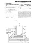
[0009] Referring to the drawing, a device 10, according to an embodiment, assembles a light receiver 30 onto a substrate 40 using a layer of conductive glue 20.
[0010] The light receiver 30 includes a first surface 31, a sensing zone 32 formed in the first surface 31, a plate-shaped first electrode 33 positioned on the first surface 31 and located outside the sensing zone 32, a second surface 34 opposite to the first surface 31, and a plate-shaped second electrode 35 covering the second surface 34.
[0011] The conductive glue 20 is applied to a surface of the second electrode 35 facing away from the second surface 34.
[0012] The substrate 40 includes a third surface 41, a soldering pad 42 positioned on the third surface 41 and corresponding to the second electrode 35 in shape and size, a fourth surface 43 opposite to the third surface 41, and a contact 44 positioned on the fourth surface 43 and electrically connected to the soldering pad 42.
[0013] The device 10 includes a tray 110, a vacuum nozzle 120, a light source 130, a driver 140, a measuring unit 150, and a controller 160.
[0014] The tray 110 defines a recess 112 for receiving the substrate 40.
[0015] The nozzle 120 attracts and holds the first surface 31 by means of a vacuum and covers the sensing zone 32. In detail, the nozzle 120 includes a holding surface 122 contacting the first surface 31 and a hole 124 defined in the holding surface 122 and communicating with a vacuum pump (not shown) to maintain a low air pressure.
[0016] The light source 130 such as a light emitting diode and a laser diode is received in the nozzle 120 (i.e., the hole 124) and emits light to illuminate the sensing zone 32. The sensing zone 32 is received within the hole 124 and exposed to the light source 130. The light receiver 30 is thus activated to generate a first electrical signal and transmit the first electrical signal out via the first electrode 33 and the second electrode 35.
[0017] The driver 140, such as a mechanical arm, is positioned around the tray 110 and is connected to the nozzle 120. The driver 140 moves the second electrode 35 to align it with the soldering pad 42 and then place the light receiver 30 onto the substrate 40.
[0018] The measuring unit 150 includes a first probe 152 and a second probe 154. The first probe 152 is buried in the tray 110 and makes electrical contact with the contact 44. The second probe 154 is connected to the nozzle 120 and contacts the first electrode 33 when the light receiver 30 is pressed by the nozzle 120 onto the substrate 40. The measuring unit 150 instantaneously measures a second electrical signal, which is a part of the first electrical signal that passes to the substrate 40 when the light receiver 30 is pressed by the nozzle 120 onto the substrate 40.
[0019] In particular, during the pressing, the conductive glue 20 is compressed and becomes thinner and thinner until the conductive glue 20 is compressed to the maximum degree. As such, electrical resistance between the light receiver 30 and the substrate 40 decreases to the most minimal amount when the conductive glue 20 is compressed to the maximum degree. Thus, the strength of the second electrical signal is at the greatest level when the conductive glue 20 is compressed to the maximum degree. That is, after the conductive glue 20 is compressed to the maximum degree, the second electrical signal remains unchanged, or can only decrease in strength, and the light receiver 30 might suffer damage from any increase in physical pressure.
[0020] The measuring unit 150 can be a charging-rate meter, an ammeter, or a voltmeter. Accordingly, the first electrical signal and the second electrical signal are charging rate, outright current, or voltage level.
[0021] The controller 160 controls the driver 140 to press the light receiver 30 according to the second electrical signal. In detail, the controller 160 controls the driver 140 to keep pressing the light receiver 30 until the second electrical signal stops increasing in strength.
[0022] As such, the device 10 can instantaneously monitor the pressing to reduce insertion loss while avoiding damage to the light receiver 30.
[0023] To increase efficiency, in other embodiments, the tray 110 can define a number of the recesses 112, which can be arrayed, for receiving a large number of the substrates 40. Accordingly the measuring unit 150 can include a number of the first probes 152 to make contact with the number of the contacts 44.
[0024] It will be understood that the above particular embodiments are shown and described by way of illustration only. The principles and the features of the present disclosure may be employed in various and numerous embodiments thereof without departing from the scope of the disclosure. The above-described embodiments illustrate the possible scope of the disclosure but do not restrict the scope of the disclosure.
User Contributions:
Comment about this patent or add new information about this topic:
| People who visited this patent also read: | |
| Patent application number | Title |
|---|---|
| 20170063567 | HEATING COOKING SYSTEM |
| 20170063566 | INTERNET OF THINGS (IOT) INTELLIGENT ELECTRONIC DEVICES, SYSTEMS AND METHODS |
| 20170063565 | SUPPORTING LOW LATENCY APPLICATIONS AT THE EDGE OF WIRELESS COMMUNICATION NETWORKS |
| 20170063564 | SUPPORTING MULTICAST IN NOC INTERCONNECT |
| 20170063563 | OPTIMIZING USER EXPERIENCES OF WEB CONFERENCES THAT SEND DATA WITH SOURCE-SPECIFIC MULTICAST AND AUTOMATIC MULTICAST TUNNELING |
Images included with this patent application:
 |  |
| Similar patent applications: | |
| Date | Title |
|---|---|
| 2015-01-08 | Device and method for assembling insulating glass panes |
| 2015-01-08 | Method of manufacturing a venting device for tamper resistant electronic modules |
| 2015-01-08 | Bundle guiding device of compressor and bundle guiding method of compressor |
| 2015-01-08 | Needle assembly removal device and disposal device |
| 2012-12-27 | Method of manufacturing coreless substrate |
| New patent applications in this class: | |
| Date | Title |
|---|---|
| 2016-04-21 | Component crimping apparatus |
| 2015-10-29 | Mems fabrication tool and method for using |
| 2014-08-28 | High load and high precision polygonal guide, and picker actuator using same |
| 2010-10-21 | Head assembly for chip mounter |
| 2010-01-21 | Nozzle unit and component mounting apparatus |
| New patent applications from these inventors: | |
| Date | Title |
|---|---|
| 2016-06-30 | Illuminating device |
| 2015-11-12 | Method for manufacturing led die |
| 2015-10-01 | Optical fiber connector with optical fiber holder received in rj45 plug |
| 2015-08-27 | Optical communication module and method for assembling same |
| 2015-08-13 | Method for adjusting circuit board |
| Top Inventors for class "Metal working" | |
| Rank | Inventor's name |
|---|---|
| 1 | Levi A. Campbell |
| 2 | Robert E. Simons |
| 3 | Branko Sarh |
| 4 | Richard C. Chu |
| 5 | Shou-Shan Fan |