Patent application title: 3D STACKING SEMICONDUCTOR DEVICE AND MANUFACTURING METHOD THEREOF
Inventors:
Shih-Hung Chen (Hsinchu County, TW)
Shih-Hung Chen (Hsinchu County, TW)
Assignees:
MACRONIX INTERNATIONAL CO., LTD.
IPC8 Class: AH01L23485FI
USPC Class:
257734
Class name: Active solid-state devices (e.g., transistors, solid-state diodes) combined with electrical contact or lead
Publication date: 2014-07-10
Patent application number: 20140191388
Abstract:
A 3D stacking semiconductor device and a manufacturing method thereof are
provided. The manufacturing method includes the following steps. N layers
of stacking structures are provided. Each stacking structure includes a
conductive layer and an insulating layer. A first photoresister layer is
provided. The stacking structures are etched P-1 times by using the first
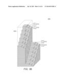
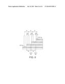
photoresister layer as a mask. A second photoresister layer is provided.
The stacking structures are etched Q-1 times by using the second
photoresister layer as a mask. The first photoresister layer is trimmed
along a first direction. The second photoresister layer is trimmed along
a second direction. The first direction is different from the second
direction. A plurality of contact points are arranged along the first and
the second directions in a matrix. The included angle between the first
direction and the second direction is an acute angle.Claims:
1. A manufacturing method of a 3D stacking semiconductor device,
comprising: providing N layers of stacking structures, wherein each
stacking structure includes a conductive layer and an insulating layer,
the conductive layers and the insulating layers are interlaced,
N≦P×Q, and N, P and Q are positive numbers; providing a
first photoresister layer, the first photoresister layer covering part of
the surface of the stacking structures; etching P-1 times the stacking
structures by using the first photoresister layer as a mask, wherein in
etch step of etching the stacking structures, the stacking structures are
etched for a thickness of one layer, and the first photoresister layer is
trimmed for a width after each of the 1 to P-2 steps of etching the
stacking structures; removing the first photoresister layer; providing a
second photoresister layer, the second photoresister layer covering part
of the surface of the stacking structures; etching Q-1 times the stacking
structures by using the second photoresister layer as a mask, wherein in
etch step of etching the stacking structures, the stacking structures are
etched for another thickness of P layers, and the second photoresister
layer is trimmed for another width after each of the 1 to Q-2 steps of
etching the stacking structures; removing the second photoresister layer;
and providing N conductive lines, each conductive line electrically
connected to one conductive point of each conductive layer; wherein the
first photoresister layer is trimmed along a first direction, the second
photoresister layer is trimmed along a second direction, the first
direction is different from the second direction, a plurality of contact
points are arranged along the first and the second directions in a
matrix, and the included angle between the first direction and the second
direction is an acute angle.
2. The manufacturing method of the 3D stacking semiconductor device according to claim 1, wherein P and Q are factors of N.
3. The manufacturing method of the 3D stacking semiconductor device according to claim 1, wherein Q is smaller then or equal to P.
4. The manufacturing method of the 3D stacking semiconductor device according to claim 1, wherein N≦P×Q×R, R is another positive number, and the manufacturing method of the 3D stacking semiconductor device further includes: providing a third photoresister layer, the third photoresister layer covering part of the surface of the stacking structures; etching R-1 times the stacking structures by using the third photoresister layer as a mask, wherein in etch step of etching the stacking structures, the stacking structures are etched for another thickness of P×Q layers, and the third photoresister layer is trimmed for another width after each of the 1 to R-2 steps of etching the stacking structures; and removing the third photoresister layer.
5. The manufacturing method of the 3D stacking semiconductor device according to claim 4, wherein P, Q and R are factors of N.
6. The manufacturing method of the 3D stacking semiconductor device according to claim 4, wherein R is smaller then or equal to Q, and Q is smaller then or equal to P.
7. The manufacturing method of the 3D stacking semiconductor device according to claim 4, wherein N≦P×Q×R×S, S is another positive number, and the manufacturing method of the 3D stacking semiconductor device further includes: providing a fourth photoresister layer, the fourth photoresister layer covering part of the surface of the stacking structure; etching S-1 times the stacking structures by using the fourth photoresister layer as a mask, in etch step of etching the stacking structures, the stacking structures are etched for another thickness of P×Q×R layers, and the fourth photoresister layer is trimmed for another width after each of the 1 to S-2 steps of etching the stacking structures; and removing the fourth photoresister layer.
8. The manufacturing method of the 3D stacking semiconductor device according to claim 7, wherein P, Q, R and S are factors of N.
9. The manufacturing method of the 3D stacking semiconductor device according to claim 7, wherein S is smaller then or equal to R, R is smaller then or equal to Q, and Q is smaller then or equal to P.
10. The manufacturing method of the 3D stacking semiconductor device according to claim 4, wherein the 3D stacking semiconductor device has a plurality of contact points, and in the step of trimming the first photoresister layer, the second photoresister layer and the third photoresister layer, a pitch between two adjacent contact points satisfies the following equation: p≧2(N-1)*dx, p is the pitch, and dx is an error quantity for which the first photoresister layer, the second photoresister layer or the third photoresister layer is trimmed.
11. A 3D stacking semiconductor device, comprising: N layers of stacking structure, each the stacking structure including: a conductive layer, wherein N is a positive number; and an insulating layer, wherein the conductive layers and the insulating layers are interlaced and stacked; and N pieces of conductive lines, wherein each conductive line is electrically connected to one contact point of each conductive layer; wherein the contact points are arranged along a first direction to form a P stages stair structure having a single layer interval, the contact points are arranged along a second direction to form a Q stages stair structure having a P stages interval, N≦P×Q, the contact points are arranged in a matrix along a first direction and a second direction, and an included angle between the first direction and the second direction is an acute angle.
12. The 3D stacking semiconductor device according to claim 11, wherein the conductive lines are straightly extended from the contact pads in parallel.
13. The 3D stacking semiconductor device according to claim 11, wherein a pitch between two adjacent contact points satisfies the following equation: p≧2(N-1)*dx, p is the pitch, and dx is an error quantity for which a photoresister layer is trimmed.
14. The 3D stacking semiconductor device according to claim 11, wherein P and Q are factors of N.
15. The 3D stacking semiconductor device according to claim 11, wherein Q is smaller then or equal to P.
16. The 3D stacking semiconductor device according to claim 11, wherein a P×Q stages stair structure is formed by the P stages stair structure and the Q stages stair structure, and the P×Q stages stair structure is arranged with P×Q stages interval along the first direction to form a P×Q×R stages structure.
17. The 3D stacking semiconductor device according to claim 16, wherein P, Q and R are factors of N.
18. The 3D stacking semiconductor device according to claim 16, wherein R is smaller then or equal to Q, and Q is smaller then or equal to P.
19. The 3D stacking semiconductor device according to claim 16, wherein the P×Q×R stages stair structure can be arranged with P×Q×R stages interval along the second direction to form a P×Q×R×S stages structure.
20. The 3D stacking semiconductor device according to claim 19, wherein P, Q, R and S are factors of N.
21. The 3D stacking semiconductor device according to claim 19, wherein S is smaller then or equal to R, R is smaller then or equal to Q, and Q is smaller then or equal to P.
Description:
BACKGROUND
[0001] 1. Technical Field
[0002] The disclosure relates in general to a semiconductor device and a manufacturing method thereof, and more particularly to a 3D stacking semiconductor device and a manufacturing method thereof.
[0003] 2. Description of the Related Art
[0004] With the development of semiconductor technology, various semiconductor elements are provided. The semiconductor elements can be installed to realize varied electric performance. Semiconductor elements are widely used in electronic products.
[0005] Under the trends of lightweight, thin, short and small, how to reduce the volume of the semiconductor element or increase the circuit density at a fixed volume becomes an important target in the semiconductor industries.
SUMMARY
[0006] The disclosure is directed to a 3D stacking semiconductor device and a manufacturing method thereof.
[0007] According to a first aspect of the present disclosure, a manufacturing method of a 3D stacking semiconductor device is provided. The manufacturing method of the 3D stacking semiconductor device comprises the following steps. N layers of stacking structures are provided. Each stacking structure includes a conductive layer and an insulating layer. The conductive layers and the insulating layers are interlaced. N≦P×Q. N, P and Q are positive numbers. A first photoresister layer is provided. The first photoresister layer covers part of the surface of the stacking structures. The stacking structures are etched P-1 times by using the first photoresister layer as a mask. In each step of etching the stacking structures, the stacking structures are etched for a thickness of one layer. The first photoresister layer is trimmed for a width at each of the 1 to P-2 steps. The first photoresister layer is removed. A second photoresister layer is provided. The second photoresister layer covers part of the surface of the stacking structures. The stacking structures are etched Q-1 times by using the second photoresister layer as a mask. In each step of etching the stacking structures, the stacking structures are etched for another thickness of P layers. The second photoresister layer is trimmed for another width of P layers after each of the 1 to Q-2 steps. The second photoresister layer is removed. N conductive lines are provided. Each conductive line is electrically connected to a contact point of each conductive layer. The first photoresister layer is trimmed along a first direction. The second photoresister layer is trimmed along a second direction. The first direction is different from the second direction. A plurality of contact points are arranged in a matrix along the first and the second directions. The included angle between the first direction and the second direction is an acute angle.
[0008] According to a second aspect of the present disclosure, a 3D stacking semiconductor device is provided. The 3D stacking semiconductor device includes N layers stacking structures and N pieces of conductive lines. Each stacking structure includes a conductive layer and an insulating layer. N is a positive number. The conductive layer and the insulating layer are interlaced and stacked. Each conductive line is electronically connected to one contact point of each conductive layer. The contact points are arranged along a first direction to form a P stages stair structure having a single layer interval. The contact points are arranged along a second direction to form a Q stages stair structure having a P stages interval. N≦P×Q. The contact points are arranged in a matrix along the first direction and the second direction. An included angle between the first direction and the second direction is an acute angle.
[0009] The above and other aspects of the disclosure will become better understood with regard to the following detailed description of the non-limiting embodiments. The following description is made with reference to the accompanying drawings.
BRIEF DESCRIPTION OF THE DRAWINGS
[0010] FIG. 1 shows a 3D stacking semiconductor device;
[0011] FIGS. 2A to 2R show a flow chart of a manufacturing method of the 3D stacking semiconductor device;
[0012] FIGS. 3A to 3B show flow chart of a manufacturing method of a 3D stacking semiconductor device;
[0013] FIGS. 4A to 4C show the change of a photoresister layer during etch and trimming;
[0014] FIG. 5 shows an arrangement of conductive lines and contact points where the conductive lines are connected to the conductive layers;
[0015] FIG. 6 shows an arrangement of conductive lines and contact points where the conductive lines are connected to the conductive layers; and
[0016] FIGS. 7 to 8 show the change of distances between the edge and the contact points.
DETAILED DESCRIPTION
[0017] Preferred embodiments are disclosed below for elaborating the invention. The following embodiments are for the purpose of elaboration only, not for limiting the scope of protection of the invention. Besides, secondary elements are omitted in the following embodiments to highlight the technical features of the invention.
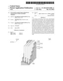
[0018] Please refer to FIG. 1, which shows a 3D stacking semiconductor device 100. The 3D stacking semiconductor device 100 includes N layers stacking structure 110 and N pieces of conductive lines 140. Each stacking structure 110 includes a conductive layer 111 and an insulating layer 112. N is a positive number. For example, N can be 18. Each conductive layer 111 has a stopping layer 120. The conductive line 140 is electronically connected to the conductive layer 111 by penetrating the stopping layer 120, for transmitting signals from the conductive layers 111 respectively. Due to the design of the 3D stacking semiconductor device 100, the N layers conductive layer 111 can be compactly stacked, and the conductive lines 140 can be arranged closely.
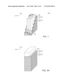
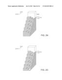
[0019] Please refer to FIGS. 2A to 2R, which shows a flow chart of a manufacturing method of the 3D stacking semiconductor device 100. In one embodiment, the 3D stacking semiconductor device 100 can be formed by a plurality of photoresister layers and a manner of trimming with multiple directions. In FIGS. 2A to 2R, the 3D stacking semiconductor device 100 with N layers of stacking structures 110 is formed by two photoresister layers and a manner of trimming with two directions.
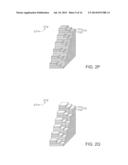
[0020] As shown in FIGS. 2A to 2E, a P stages stair structure is formed by a first photoresister layer 810. P is a positive number. For example, P can be 3. As shown in FIGS. 2F to 2P, a Q stages stair structure is formed by a second photoresister layer 820. Q is another positive number. For example, Q can be 6. N≦P×Q. For example, 18≦3×6. Hereafter, N, P and Q are exemplified by 18, 3 and 6 respectively.
[0021] In FIG. 2A, the stacking structures 110 are provided. At this time, 18 layers of stacking structures 110 are not etched. 18 layers of conductive layer 111 and 18 layers of insulating layer 112 are interlaced and stacked compactly.
[0022] In FIG. 2A, the first photoresister layer 810 is provided. The first photoresister layer 810 covers part of the surface of the 18 layers of stacking structure 110.
[0023] In FIG. 2B, the stacking structures 110 are etched by using the first photoresister layer 810 as a mask. In this step of etching the stacking structures 110, the exposed portion of the stacking structures 110 is etched for a thickness of one layer.
[0024] In FIG. 2C, the first photoresister layer 810 is trimmed for a width along a first direction C11, such that two layers of the stacking structures 110 are exposed.
[0025] In FIG. 2D, the stacking structures 810 are etched by using the trimmed first photoresister layer 810 as a mask. In this step of etching the stacking structure, the exposed portion of the stacking structures 110 is etched for a thickness of one layer. That is to say, part of the first layer and the second layer of the stacking structures 110 are etched for a thickness of one layer.
[0026] In FIG. 2E, the first photoresister layer 810 is removed to form 3 stages.
[0027] In FIGS. 2A to 2E, the stacking structures 110 are etched 2 times (i.e. P-1 times). In etch step of etching, the exposed portion of the stacking structures 110 is etched for a thickness of one layer, and the first photoresister layer 810 is trimmed for a width along the first direction C11 after the first step (i.e. the P-2 step) of etching the stacking structures 110. In FIGS. 2A to 2E, it is exemplified by 3 stages. If the process is inferred to P stages, then the stacking structures 110 are etched P-1 times by using the first photoresister layer 810 as a mask. In each step of etching the stacking structures 110, the stacking structures 110 are etched for a thickness of one layer, and the first photoresister layer 810 is trimmed for a width along the first direction after each of the 1 to P-2 steps of etching the stacking structures 110.
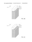
[0028] Afterwards, in FIG. 2F, the second photoresister layer 820 is provided. The second photoresister layer 820 covers part of the surface of the stacking structures 110.
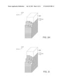
[0029] In FIG. 2G, the stacking structures 110 are etched by using the second photoresister layer 820 as a mask. In this step of etching the stacking structures 110, the exposed portion of the stacking structures 110 is etched for a thickness of 3 layers. That is to say, part of the 1 to 3 layers of the stacking structures 110 are etched for a thickness of 3 layers at the same time.
[0030] In FIG. 2H, the second photoresister layer 820 is trimmed for a width along a second direction C12, such that 6 layers of the stacking structures 110 are exposed.
[0031] In FIG. 2I, the stacking structures 110 are etched by using the trimmed second photoresister layer 820 as a mask. In this step of etching the stacking structure 110, the exposed portion of the stacking structures 110 is etched a thickness of 3 layers. That is to say, part of the 1 to 6 layers of the stacking structures 110 are etched for a thickness of 3 layers at the same time.
[0032] In FIG. 2J, the second photoresister layer 820 is trimmed for a width along the second direction C12, such that 9 layers of the stacking structures 110 are exposed.
[0033] In FIG. 2K, the stacking structures 110 are etched by using the trimmed second photoresister layer 820 as a mask. In this step of etching the stacking structure 110, the exposed portion of the stacking structures 110 is etched for a thickness of 3 layers. That is to say, part of the 1 to 9 layers of the stacking structures 110 are etched for a thickness of 3 layers at the same time.
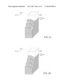
[0034] In FIG. 2L, the second photoresister layer 820 is trimmed for a width along the second direction C12, such that 12 layers of the stacking structure 110 are exposed.
[0035] In FIG. 2M, the stacking structures 110 are etch by using the trimmed second photoresister layer 820 as a mask. In this step of etching the stacking structures 110, the exposed portion of the stacking structures 110 is etched for a thickness of 3 layers. That is to say, part of the 1 to 12 layers of the stacking structures 110 are etched for a thickness of 3 layers at the same time.
[0036] In FIG. 2N, the second photoresister layer 820 is trimmed for a width along the second direction C12, such that 15 layers of the stacking structures 110 are exposed.
[0037] In FIG. 2O, the stacking structures 110 are etched by using the trimmed second photoresister layer 820 as a mask. In this step of etching the stacking structure, the exposed portion of the stacking structure 110 is etched for a thickness of 3 layers. That is to say, part of the 1 to 15 layers of the stacking structure 110 are etched for a thickness of 3 layers.
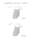
[0038] In FIG. 2P, the second photoresister layer 820 is remove to form 18 stages.
[0039] In FIGS. 2F to 2P, the stacking structures 110 are etched 5 times (i.e. Q-1 times). In each step of etching the stacking structure, the exposed portion of the stacking structures 110 is etched for a thickness of 3 layers (i.e. P layers), and the second photoresister layer 820 is trimmed for a width along the second direction C12 after each of the 1 to 4 steps (i.e. the 1 to Q-2 steps) of etching the stacking structure 110. In FIGS. 2E to 2P, it is exemplified by 6 stages. If the process is inferred to Q stages, then the stacking structures 110 are etched Q-1 times by using the second photoresister layer 820 as a mask. In each step of etching the stacking structures 110, the stacking structures 110 are etched for a thickness of P layers, and the second photoresister layer 820 are trimmed for a width along the second direction C12 after each of the 1 to Q-2 steps of etching the stacking structure 110.
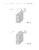
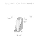
[0040] In FIG. 2Q, a plurality of stopping layer 120 are formed on the exposed portion of the stacking structure 110.
[0041] In FIG. 2R, a plurality of stopping layer 120 are formed on the exposed conductive layer 111 of the stacking structures 110, and a plurality of conductive lines 140 are provided for electronically connected to the conductive layer 111 by penetrating the stopping layer 120.
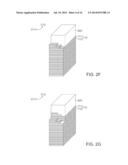
[0042] As such, 18 stages can be formed in the 3D stacking semiconductor device 100 with small volume. In FIGS. 2A to 2E, the first photoresister layer 810 is trimmed for a width along the first direction C11; in FIGS. 2F to 2P, the second photoresister layer 820 is trimmed for another width along the second direction C12. The first direction C11 is different from the second direction C12, such that the several stages can be formed along the first direction C11 and the second direction C12 to interlace a stairs matrix.
[0043] In FIGS. 2A to 2R, the included angle between the first direction C11 and the second direction C12 is exemplified by a right angle. In one embodiment, the included angle between the first direction C11 and the second direction C12 can be an acute angle.
[0044] In the present embodiment, the 3D stacking semiconductor device 100 has N layers of stacking structures 110, there is the P stages stair structure having single layer interval located along the first direction C11, and there is the Q stages stair structure having P stages interval located along the second direction C12. In the present embodiment, N, P and Q are exemplified by 18, 3 and 6 respectively. In one embodiment, N, P and Q can be 18, 6 and 3; or 18, 9 and 2, on condition that P and Q are factors of N.
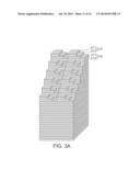
[0045] In the above embodiments, the 3D stacking semiconductor device 100 is formed by two modules process, such as P stages and Q stages. In another embodiment, a 3D stacking semiconductor device 200 can be formed by three modules process, such as P stages, Q stages and R stages. Please refer to FIGS. 3A to 3B, which show a flow chart of a manufacturing method of the 3D stacking semiconductor device 200. In FIG. 3A, a P×Q stages stair structure formed by the P stages stair structure and the Q stages stair structure, such as 3×6 stages stair structure, can be formed by a process similar to FIGS. 2A to 2R.
[0046] In FIG. 3B, a third photoresister layer 830 is provided. The third photoresister layer 830 covers part of the stacking structures 210. Each stacking structure 210 includes a conductive layer 211 and an insulating layer 212. Afterwards, the stacking structures 210 are etched by using the third photoresister layer 830 as a mask. In each step of etching the stacking structures 210, the stacking structures 210 are etched for a thickness of 18 layers. In FIGS. 3A to 3B, it is exemplified by 2 stages. If the process is inferred to R stages, then the stacking structures 210 are etched R-1 times by using the third photoresister layer 830 as a mask, in each step of etching the stacking structure 210, the stacking structures 210 are etched for a thickness of P×Q layers, and the third photoresister layer 830 is trimmed for a width after each of the 1 to R-2 steps of etching the stacking structure 210.
[0047] That is to say, a 3D stacking semiconductor device having N stages can be formed by three modules process, such as P stages, Q stages and R stages. P×Q stages stair structure can be arranged with P×Q stages interval along the first direction to form a P×Q×R stages structure. N, P, Q and R are positive numbers, N≦P×Q×R, and P, Q and R are factors of N.
[0048] Similarly, if the process is inferred next, 3D stacking semiconductor device having N stages can be formed by four modules process, such as P stages, Q stages, R stages and S stages. The P×Q×R stages stair structure can be arranged with P×Q×R stages interval along the second direction to form a P×Q×R×S stages structure. N, P, Q, R and S are positive numbers, N≦P×Q×R×S, and P, Q, R and S are factors of N. After P stages, Q stages and R stages of the 3D stacking semiconductor device are formed, a fourth photoresister layer can be provided. The fourth photoresister layer covers part of the stacking structures. Then, the stacking structures are etched S-1 times by using the fourth photoresister layer as a mask. In each steps of etching the stacking structures, the stacking structures are etched for a thickness of P×Q×R layers. The fourth photoresister layer is trimmed for a width after the each of the 1 to S-2 steps of etching the stacking structures.
[0049] According to the similar manners, a 3D stacking semiconductor device can be formed by more than five modules process.
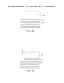
[0050] Please refer to FIGS. 4A to 4C, which show the change of a photoresister layer 910 during etch and trimming. As shown in FIGS. 4A to 4B, the photoresister layer 910 will be consumed for a thickness h1, such as about 500 Å, during the process of etching the stacking structure 310. As shown in FIGS. 4B to 4C, the photoresister layer 910 will be consumed for a thickness t1, such as about 4000 Å, during the process of trimming the photoresister layer 910 for a width tx. Thus, the consumption of the photoresister layer 910 is needed to be controlled during the steps of etching or the steps of trimming.
[0051] Take table 1 as an example, N is 36 and 3D stacking semiconductor device having 36 stages is formed by one module process. The number of trimming times is 34, and the number of etched layers is 35. The total consumption of the photoresister layer is 153500 Å.
TABLE-US-00001 TABLE 1 first module process first module number of number of total process trimming etched consumption serial numbers N P times layers (Å) 1-1 36 36 36 35 153500
[0052] Take table 2A as an example, N is 36 and 3D stacking semiconductor device having 36 stages is formed by two modules process. The first module process and the second module process can be exemplified by several combinations of P and Q, such as the combinations of No. 2-1, 2-2 and 2-3. As shown in table 2B, when the 6 stages are formed in the first module process and 6 stages are formed in the second module process, the total consumption is lowest.
[0053] Because the consumption of the photoresister layer in the second module process is larger than that in the first module process. Thus, Q≦P is a better choice according to the total consumption of the photoresister layer. For example, in number 2-1 of table 2B, the consumption of the photoresister layer in the first module process is 9500 Å, and the consumption of the photoresister layer in the second module process is 44000 Å which is very high. Besides, the problems under a thick photoresister layer are the decreasing of the optical resolution and the limit of the thickness of the photoresister layer. Therefore, number 2-1 is not the best case. Numbers 2-2 or 2-3 are the better cases.
TABLE-US-00002 TABLE 2A first module second module process process serial numbers N P Q 2-1 36 4 9 2-2 36 6 6 2-3 36 9 4
TABLE-US-00003 TABLE 2B first module process second module process total serial number of number of Consumption number of number of Consumption consumption number trimming times etched layers (Å) trimming times etched layers (Å) (Å) 2-1 2 3 9500 7 32 44000 53500 2-2 4 5 18500 4 30 31000 49500 2-3 7 8 32000 2 27 21500 53500
[0054] Take table 3A as an example, N is 36 and 3D stacking semiconductor device having 36 stages is formed by three modules process. The first module process, the second module process and the third module process can be exemplified by several combinations of P, Q and R, such as the combinations of No. 3-1, 3-2, 3-3 and 3-4. As shown in tables 3B to 3C, when the 3 stages are formed in the first module process, 3 stages are formed in the second module process and 4 stages are formed in the third module process, the total consumption is lowest.
[0055] Usually, the reason to enter a next module process is that the thickness of the photoresister layer is reached a limit thereof, the accuracy is decreased due to the trimming or an enlarging requirement base on the design rule. For example, if the limit of the thickness of the photoresister layer is 20000 Å, then there is no case which can be selected, and only numbers 3-2 and 3-4 can be selected in tables 3B to 3C.
[0056] Moreover, the consumption of the photoresister layer in the third module process is larger than that in the second module process. Thus, R≦Q≦P is a better choice according to the total consumption of the photoresister layer.
[0057] According to the similar manners, on the case which four modules process are applied, S≦R≦Q≦P is the better choice.
TABLE-US-00004 TABLE 3A second first module module third module serial process process process numbers N P Q R 3-1 36 3 6 2 3-2 36 6 3 2 3-3 36 3 3 4 3-4 36 4 3 3
TABLE-US-00005 TABLE 3B first module process second module process number number number number serial of of consump- of of consump- num- trimming etched tion trimming etched tion bers times layers (Å) times layers (Å) 3-1 1 2 5000 4 15 23500 3-2 4 5 18500 1 12 10000 3-3 1 2 5000 1 6 7000 3-4 2 3 9500 1 8 8000
TABLE-US-00006 TABLE 3C third module process number of total serial trimming number of Consumption consumption numbers times etched layers (Å) (Å) 3-1 0 18 9000 37500 3-2 0 18 9000 37500 3-3 2 27 21500 33500 3-4 1 24 16000 33500
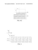
[0058] Please refer to FIG. 5, which shows an arrangement of a plurality of conductive lines 440 and a plurality of contact points 411a where the conductive lines 440 are connected to the conductive layers 411. The above described 3D stacking semiconductor device can include a plurality of conductive layers 411 stacked compactly and a plurality of contact pads 411a where the conductive lines 440 are connected to the conductive layers 411 arranged closely. Because the photoresister layer are trimmed along the first direction C41 and the second direction C42, the contact points 411a are arranged along the first direction C11 and the second direction C12 in a matrix accordingly. If an included angle θ1 between the first direction C41 and the second direction C42 is a substantially right angle, then the conductive lines 440 must be formed as L shaped to stagger the same.
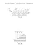
[0059] Please refer to FIG. 6, which shows an arrangement of a plurality of conductive lines 540 and a plurality of contact points 511a where the conductive lines 540 are connected to the conductive layers 511. The above described 3D stacking semiconductor device can include a plurality of conductive layers 511 stacked compactly and a plurality of contact points 511a where the conductive lines 540 are connected to the conductive layers 511 arranged closely. Because the photoresister layer are trimmed along the first direction C51 and the second direction C52, the contact points 511a are arranged along the first direction C51 and the second direction C52 in a matrix accordingly. If an included angle 82 between the first direction C51 and the second direction C52 is an acute angle, then the conductive lines 540 can be straightly extended from the contact pads 511a in parallel and do not need to be formed as L shaped to stagger the same.
[0060] Besides, when the included angle 82 between the first direction C51 and the second direction C52 is an acute angle, the width tx for which the photoresister layer is trimmed becomes width tx'. The width tx' is sin θ2 times the width tx.
[0061] Moreover, please referring to FIGS. 7 to 8, the change of distances D1, D2 and D3 between the edge and the contact points 611a is shown. Pitches between any two adjacent contact points 611a are equal. As shown in FIG. 7, under an ideal case, the width tx for which the photoresister layer is trimmed is fixed. Therefore, in FIG. 7, the distances D1, D2 and D3 between the edge and the contact points 611a can be fixed at p/2.
[0062] As shown in FIG. 8, there is an error quantity dx for which a photoresister layer is trimmed. Therefore, in FIG. 8, the distance D2 between the edge and the contact point 611a becomes p/2-dx, the distance D3 between the edge and the contact point 611a becomes p/2-2dx, and so on. After the N layers of stacking structures 110 is trimmed N-1 times, the distance between the edge and the contact point 611a becomes p/2-(N-1)*dx. The distance between the edge and the contact point is needed to be larger than zero; therefore, the pitch p is needed to be larger than 2(N-1)*dx.
[0063] While the disclosure has been described by way of example and in terms of the exemplary embodiment(s), it is to be understood that the disclosure is not limited thereto. On the contrary, it is intended to cover various modifications and similar arrangements and procedures, and the scope of the appended claims therefore should be accorded the broadest interpretation so as to encompass all such modifications and similar arrangements and procedures.
User Contributions:
Comment about this patent or add new information about this topic:
Images included with this patent application:
 |  |
 |  |
 |  |
 |  |
 |  |
 |  |
 |  |
 |  |
 |  |
| Similar patent applications: | |
| Date | Title |
|---|---|
| 2010-12-16 | System and method for reducing process-induced charging |
| 2014-04-17 | Semiconductor device |
| 2014-04-17 | Semiconductor device |
| 2014-04-17 | Semiconductor device |
| 2014-04-24 | Semiconductor device |
| New patent applications in this class: | |
| Date | Title |
|---|---|
| 2019-05-16 | Semiconductor wafer and semiconductor wafer fabrication method |
| 2016-06-09 | Semiconductor package and method of manufacturing the same |
| 2016-06-02 | Electronic device and method for manufacturing same |
| 2016-04-28 | Anodized metal on carrier wafer |
| 2016-04-21 | Layer-selective laser ablation patterning |
| New patent applications from these inventors: | |
| Date | Title |
|---|---|
| 2022-08-04 | Three-way switch array structure and switch array substrate based on nvm |
| 2017-02-16 | Memory device comprising memory strings penetrating through a stacking structure and electrically contacting with a metal layer and method for fabricating the same |
| 2017-02-16 | Connector structure and method for fabricating the same |
| 2016-01-07 | Three dimensional stacked multi-chip structure and manufacturing method of the same |
| 2015-07-23 | Three-dimensional semiconductor device |
| Top Inventors for class "Active solid-state devices (e.g., transistors, solid-state diodes)" | |
| Rank | Inventor's name |
|---|---|
| 1 | Shunpei Yamazaki |
| 2 | Shunpei Yamazaki |
| 3 | Kangguo Cheng |
| 4 | Huilong Zhu |
| 5 | Chen-Hua Yu |