Patent application title: Programmable Gamma Circuit of Liquid Crystal Display Driving System
Inventors:
Wei Fu (Shenzhen City, CN)
Nianmao Wang (Shenzhen City, CN)
Assignees:
SHENZHEN CHINA STAR OPTOELECTRONICS TECHNOLOGY CO., LTD.
IPC8 Class: AG06F126FI
USPC Class:
345211
Class name: Computer graphics processing and selective visual display systems display driving control circuitry display power source
Publication date: 2014-06-26
Patent application number: 20140176519
Abstract:
A programmable gamma circuit of liquid crystal display driving system,
comprises: a first digital-to-analog converter to a n-th
digital-to-analog converter, which receive a data used to generate a
reference voltage of a pixel grayscale from a timing controller of the
liquid crystal display driving system and convert the data to an analog
signal; a first operational amplifier to a n-th operational amplifier,
each operational amplifier being connected to a corresponding
digital-to-analog converter, the amplified analog signal being the
reference voltage of the pixel grayscale ; a first resistor to a fifth
resistor, which are connected in series with each other, the operating
voltage obtained by a voltage converter of the liquid crystal display
driving system converting the reference voltage being input to one end of
the first resistor, and one end of the fifth resistor being grounded. The
voltage between the first resistor and the second resistor is input
respectively to the power supply terminals of the first n/2 operational
amplifiers, the voltage between the second resistor and the third
resistor is input respectively to the ground terminals of the first n/2
operational amplifiers, the voltage between the third resistor and the
fourth resistor is input respectively to the power supply terminals of
the last n/2 operational amplifier, and the voltage between the fourth
resistor and the fifth resistor is input respectively to the ground
terminals of the last n/2 operational amplifier.Claims:
1. A programmable gamma circuit of liquid crystal display driving system,
comprising: a first digital-to-analog converter to a n-th
digital-to-analog converter, which receive a data used to generate a
reference voltage of a pixel grayscale from a timing controller of the
liquid crystal display driving system and convert the data to an analog
signal; a first operational amplifier to a n-th operational amplifier,
each operational amplifier being connected to a corresponding
digital-to-analog converter within the first digital-to-analog converter
to the n-th digital-to-analog converter, the analog signal converted by
the first operational amplifier converter to the n-th operational
amplifier converter being the reference voltage of the pixel grayscale
Vout1 to Voutn, wherein, n is even; a first resistor to a fifth
resistor, which are connected in series with each other, the operating
voltage VAA obtained by a voltage converter of the liquid crystal
display driving system converting the reference voltage being input to
one end of the first resistor, and one end of the fifth resistor being
grounded; wherein, the voltage VAA1 between the first resistor and
the second resistor is input respectively to the power supply terminals
of the first n/2 operational amplifiers, the voltage VAA2 between
the second resistor and the third resistor is input respectively to the
ground terminals of the first n/2 operational amplifiers, the voltage
VAA3 between the third resistor and the fourth resistor is input
respectively to the power supply terminals of the last n/2 operational
amplifier, and the voltage VAA4 between the fourth resistor and the
fifth resistor is input respectively to the ground terminals of the last
n/2 operational amplifier.
2. The programmable gamma circuit as claimed in claim 1, wherein the voltage VAA1 between the first resistor and the second resistor is greater than the reference voltage Vout1 of the pixel grayscale output from the first operational amplifier, the voltage VAA2 between the second resistor and the third resistor is less than the reference voltage Vout(n/2-1) output from the pixel grayscale of the (n/2-1)-th operational amplifier, the voltage VAA3 between the third resistor and the fourth resistor is greater than the reference voltage Vout(n/2-1) of the pixel grayscale output from the (n/2-1)-th operational amplifier, the voltage VAA4 between the fourth resistor and a fifth resistor is less than the reference voltage Voutn output from the pixel grayscale of the n-th operational amplifier.
3. The programmable gamma circuit as claimed in claim 1, wherein the resistances R1 to R5 of the first resistor to the fifth resistor satisfy the equation: VAA/(R1+R2+R3+R4+R5)=VAA1/(R2+R.s- ub.3+R4+R5)=VAA2/(R3+R4+R5)=VAA3/(R.sub- .4+R5)=VAA4/R5, determine the values of the voltage VAA1 to VAA4 according to the values of the predetermined reference voltage Vout1 to Voutn of the pixel grayscale, then select the resistance R5 of the fifth resistor, and calculate the resistances R1 to R4 of the first resistor to the fourth resistor according to the equation.
Description:
BACKGROUND OF THE INVENTION
[0001] 1. Field of the Invention
[0002] The present invention belongs to the field of liquid crystal display, which relates to a programmable gamma circuit of a liquid crystal display reducing the power consumption and the temperature.
[0003] 2. The Related Arts
[0004] The driving system of the known liquid crystal display (LCD) typically comprises a programmable Gamma (P-Gamma) circuit. The P-Gamma circuit generates a pixel grayscale voltage reference (Gamma voltage). The pixel grayscale reference voltage can be supplied to the gate driver in order to drive each pixels of the liquid crystal display panel.
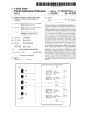
[0005] FIG. 1 is a partial block diagram of the driving system according to the known LCD. Referring to FIG. 1, the interface logic 1 of a inter integrated circuit (12C) receives serial clock (SCL) signal, serial data (SDA) and writing enable signal (nWR), and supplies the received signals and the data to a timing controller 2. The timing controller 2 generates a timing control signal and a data used to generate the reference voltage of the pixel grayscale. P-Gamma circuit 3 comprises multiple digital-to-analog converters (DAC) and multiple OPs, each DAC is connected to a corresponding OP. DAC receives the data used to generate the reference voltage of the pixel grayscale from the timing controller 2, and converts the data to a analog signal. The analog signals amplified and converted from the OP act as the reference voltages Vout1 Vout2 of . . . , Voutn (FIG. 1 shows the situation that the n is 14) of the pixel grayscale. The timing controller 2 controls the timing of the reference voltage of the pixel grayscale generated by each OP according to the timing control signal. Moreover, the deflecting reference voltage of the liquid crystal molecules (Vcom) module 4 generates the deflecting reference voltage Vcom out of the liquid crystal molecules according to the timing controller 2.
[0006] Typically, the working voltage of the OP in the P-Gamma circuit is VAA/0 (VAA is the operating voltage converted from the reference voltage by the voltage converter of the LCD driving system). The voltage difference of the OP is larger, and the power consumption P of the OP=V (voltage)×I (current), so that the power consumption of OP is larger, the power consumption of the corresponding P-Gamma circuit will be larger, and the temperature of the P-Gamma circuit is also higher, which will reduce the performance of the P-Gamma circuit and decrease the life of the P-Gamma circuit.
SUMMARY OF THE INVENTION
[0007] According to an aspect of the present invention, it provides a programmable gamma circuit of liquid crystal display driving system, comprising: a first digital-to-analog converter to a n-th digital-to-analog converter, which receive a data used to generate a reference voltage of a pixel grayscale from a timing controller of the liquid crystal display driving system and convert the data to an analog signal; a first operational amplifier to a n-th operational amplifier, each operational amplifier being connected to a corresponding digital-to-analog converter within the first digital-to-analog converter to the n-th digital-to-analog converter, the analog signal converted by the first operational amplifier converter to the n-th operational amplifier converter being the reference voltage of the pixel grayscale Vout1 to Voutn, wherein, n is even; a first resistor to a fifth resistor, which are connected in series with each other, the operating voltage VAA obtained by a voltage converter of the liquid crystal display driving system converting the reference voltage being input to one end of the first resistor, and one end of the fifth resistor being grounded; wherein, the voltage VAA, between the first resistor and the second resistor is input respectively to the power supply terminals of the first n/2 operational amplifiers, the voltage VAA2 between the second resistor and the third resistor is input respectively to the ground terminals of the first n/2 operational amplifiers, the voltage VAA3 between the third resistor and the fourth resistor is input respectively to the power supply terminals of the last n/2 operational amplifier, and the voltage VAA4 between the fourth resistor and the fifth resistor is input respectively to the ground terminals of the last n/2 operational amplifier.
[0008] The voltage VAA1 between the first resistor and the second resistor is greater than the reference voltage Vout1 of the pixel grayscale output from the first operational amplifier, the voltage VAA2 between the second resistor and the third resistor is less than the reference voltage Vout(n/2-1) output from the pixel grayscale of the (n/2-1)-th operational amplifier, the voltage VAA3 between the third resistor and the fourth resistor is greater than the reference voltage Vout(n/2-1) of the pixel grayscale output from the (n/2-1)-th operational amplifier, the voltage VAA4 between the fourth resistor and a fifth resistor is less than the reference voltage Voutn output from the pixel grayscale of the n-th operational amplifier.
[0009] The resistances R1 to R5 of the first resistor to the fifth resistor satisfy the equation: VAA/(R1+R2+R3+R4+R5)=VAA1/(R2+R.s- ub.3+R4+R5) =VAA2/(R3+R4+R5)=VAA3/(R4+R5)=VAA- 4/R5, determine the values of the voltage VAA1 to VAA4 according to the values of the predetermined reference voltage Vout1 to Voutn of the pixel grayscale, then select the resistance R5 of the fifth resistor, and calculate the resistances R1 to R4 of the first resistor to the fourth resistor according to the equation.
BRIEF DESCRIPTION OF THE DRAWINGS
[0010] From the following description of the embodiments accompanying with the drawings, the present invention and/or other aspects and advantages will become apparent and more easy to be understood, wherein:
[0011] FIG. 1 is a partial block diagram of the driving system according to the known LCD;
[0012] FIG. 2 is a schematic view illustrating a P-Gamma circuit of the driving system of the LCD according to the first embodiment of the present invention; and
[0013] FIG. 3 is a block diagram of the P-Gamma circuit of the driving system of the LCD according to the second embodiment of the present invention.
DETAILED DESCRIPTION OF THE PREFERRED EMBODIMENTS
[0014] The following embodiment of the present invention will be described in detail accompanying with the drawings.
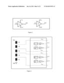
[0015] FIG. 2 is a schematic view illustrating a P-Gamma circuit of the driving system of the LCD according to the first embodiment of the present invention.
[0016] Referring to FIG. 2, in the first embodiment of the present invention, import the half of the operating voltage VAA (HVAA) converted from the reference voltage by the voltage converter of the LCD driving system as the working voltage of the OP in P-Gamma circuit.
[0017] Specifically, P-Gamma circuit comprises the first DAC to the n-th DAC and the first OP to the n-th OP, wherein n is even (see FIG. 3). Each DAC is connected to a corresponding OP. Each OP is connected to a corresponding DAC. The DAC receives the data used to generate the reference voltage of the pixel grayscale from the timing controller of the LCD driving system, and converts the data to an analog signal. The analog signal amplified and converted by the OP is used for the reference voltages of the pixel grayscale Vout1, Vout2, . . . , Voutn.
[0018] Divide the n OPs into two groups of first n/2 OPs and last n/2 OPs. The following takes n equal to 14 as an example to describe the first embodiment of the present invention. The present invention is not limited thereto, and the size of the n can be changed according to the requirement. Divide the 14 OPs into two groups of the first 7 OPs and the last 7 OPs. Import the half of the operating voltage VAA (HVAA) converted from the reference voltage by the voltage converter of the LCD driving system. The operating voltage VAA is input respectively to the power supply terminals of the first 7 OPs, and the half of operating voltage VAA (HVAA) is input respectively to the ground terminal of the first 7 OPs; similarly, the half of operating voltage VAA (HVAA) is input respectively to the power supply terminals of the other 7 OPs, and the ground terminals of the last 7 OPs are grounded (i.e. the voltage is 0).
[0019] Therefore, the working voltage across the OP is only half of the working voltage according to the known technologies. The current flowing through the OP is decided by the load connected to the OP backend. If the load is same, the current flowing through the OP will not be changed. According to power consumption P=V×I, in theory, the power consumption of each OP will be reduced by half, and the temperature will be reduced. Therefore, the power consumption of the P_Gamma circuit will be reduced, and the temperature will be reduced.
[0020] It can directly generate half the operating voltage VAA (HVAA) through the voltage converter of the LCD driving system, or it can generate half the operating voltage VAA (HVAA) through connecting two identical voltage-dividing resistors in series.
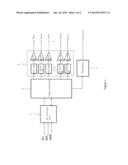
[0021] FIG. 3 is a block diagram of the P-Gamma circuit of the driving system of the LCD according to the second embodiment of the present invention.
[0022] Referring to FIG. 3, the P-Gamma circuit comprises the first DAC converter to the n-th DAC and the first OP to the n-th OP, wherein n is even. Each DAV is connected to a corresponding OP. Each OP is connected to a corresponding DAC. The first DAC to the n-th DAC receive the data used to generate the reference voltage of the pixel grayscale from the timing controller of the LCD driving system, and convert the data to an analog signal. The analog signal amplified and converted by OP is used for the reference voltage of the pixel grayscale Vout1, Vout2. . . , Voutn.
[0023] Divide the n OPs into two groups of first n/2 OPs and last n/2 OPs. The following takes n equal to 14 as an example to describe the second embodiment of the present invention. The present invention is not limited thereto, and the size of the n can be changed according to the requirement. Divide the 14 OPs into two groups of the first 7 OPs and the last 7 OPs.
[0024] In the second embodiment of the present invention, import the first resistor R1 to the fifth resistor R5 to divide the operating voltage VAA.
[0025] Specifically, the first resistor R1 to the fifth resistor R5 are connected with each other in series, the operating voltage VAA is input to one end of the first resistor R1, and one end of the fifth resistor R5 is grounded.
[0026] The voltage VAA1 between the first resistor R1 and second resistor R2 is respectively input to the power supply terminals of the first 7 OP, the voltage VAA2 between the second resistor R2 and the third resistor R3 is respectively input to the ground terminals of the first 7 OP, the voltage VAA3 between the third resistor R3 and the fourth resistor R4 is respectively input to the power supply terminals of the last 7 OP, the voltage VAA4 between the fourth resistor R4 and the fifth resistor R5 is respectively input to the ground terminals of the last 7 OP. In this way, the voltage differences of the first 7 OP are VAA1-VAA2, the voltage differences of the last 7 OP are VAA3-VAA4, both (VAA1-VAA2) and (VAA3-VAA4) are less than VAA.
[0027] The operating voltages of each OP are couple, one is high and the other one is low, the output voltage Vout of the OP is provided within the working voltages of the OPs. Therefore, VAA1>Vout1, VAA2<Vout7, VAA3>Vout8, VAA4<Vout14. In the case of the n OP, it is similar to obtain VAA1>Vout1, VAA2<Vout(n/2-1), VAA3>Vout(n/2+1), VAA4<Voutn.
[0028] According to the relationship of the first resistor R1 to the fifth resistor R5 connected in series to each other, it can be known that VAA/(R1 +R2+R3+R4+R5)=VAA1/(R2+R3+R4+R.su- b.5)=VAA2/(R3+R4+R5)=VAA3/(R4+R5)=V.sub- .AA4/R5. Here it also uses R1 to R5 to represent the resistances of the first resistor to the fifth resistor.
[0029] Therefore, it can determine the value of VAA1 to VAA4 according to each required reference voltage of the pixel grayscale Vout1, Vout2, . . . , Vout14, and then select the resistance of the fifth resistor R5, and it can calculate the resistances of the first resistor to the fourth resistor according to the above equation.
[0030] As mentioned above, the current flowing through the OP is decided by the load connected to OP backend. If load is same, the current flowing through the OP will not be changed. According to power consumption P=V×I, if V is reduced, in theory, the power consumption on each OP will be reduced, and the temperature will be reduced. Thus, the power consumption of P_Gamma circuit will be reduced, and the temperature will be reduced. Accordingly, it can maintain the performance of the P-Gamma circuit and prolong the life of the P-Gamma circuit.
[0031] The present invention referring to the exemplary embodiment is specifically described and illuminated, but those having ordinary skills in the art should understand that it can changed in various forms and details without departing from the spirit and scope of the claim defined by the present invention.
User Contributions:
Comment about this patent or add new information about this topic:
Images included with this patent application:
 |  |
 |
| Similar patent applications: | |
| Date | Title |
|---|---|
| 2014-07-17 | Stereoscopic image generating method, stereoscopic image generating device, and display device having same |
| 2014-07-10 | Liquid crystal display device |
| 2014-07-03 | Stutter buffer transfer techniques for display systems |
| 2014-07-10 | Area-saving driving circuit for display panel |
| 2014-07-17 | Pixel and organic light emitting display using the same |
| New patent applications in this class: | |
| Date | Title |
|---|---|
| 2022-05-05 | Display substrate and display device |
| 2022-05-05 | Head mounted display device and power management method thereof |
| 2017-08-17 | Driving method of a liquid crystal display panel and liquid crystal display device |
| 2017-08-17 | Driving circuit and liquid crystal display device |
| 2017-08-17 | Data driver and a display apparatus having the same |
| New patent applications from these inventors: | |
| Date | Title |
|---|---|
| 2015-01-22 | Liquid crystal device and the driven method thereof |
| 2014-11-20 | Chamfered circuit and control method thereof |
| 2014-07-17 | Gate driver and liquid crystal display device |
| Top Inventors for class "Computer graphics processing and selective visual display systems" | |
| Rank | Inventor's name |
|---|---|
| 1 | Katsuhide Uchino |
| 2 | Junichi Yamashita |
| 3 | Tetsuro Yamamoto |
| 4 | Shunpei Yamazaki |
| 5 | Hajime Kimura |