Patent application title: ARYLOXYALKYLCARBOXYLATE SOLVENT COMPOSITIONS FOR INKJET PRINTING OF ORGANIC LAYERS
Inventors:
Kwang-Ohk Cheon (Holland, PA, US)
Kwang-Ohk Cheon (Holland, PA, US)
Angang Dong (Ewing, PA, US)
Michael Inbasekaran (Lawrenceville, NJ, US)
Suman Layek (Lawrenceville, NJ, US)
Suman Layek (Lawrenceville, NJ, US)
Assignees:
Universal Display Corporation
IPC8 Class: AH01B112FI
USPC Class:
257 40
Class name: Active solid-state devices (e.g., transistors, solid-state diodes) organic semiconductor material
Publication date: 2014-04-10
Patent application number: 20140097406
Abstract:
A liquid composition (e.g., inkjet fluid) for forming an organic layer of
an organic electronic device (e.g., an OLED). The liquid composition
comprises a small molecule organic semiconductor material mixed in a
solvent in which the solvent compound has the following formula:
##STR00001##
wherein R1 is C1-6 alkyl; R2 is C1-6 alkyl; and
R3 is one or more optional substitutions independently selected from
C1-6 alkyl and lower aryl.Claims:
1. A liquid composition comprising: a small molecule organic
semiconductor material at a concentration in the range of 0.01-10 wt %;
and a solvent having a melting point of 25.degree. C. or lower, the
solvent compound having the following formula: ##STR00112## wherein
R1 is C1-6 alkyl; R2 is C1-6 alkyl; and R3 is
one or more optional substitutions independently selected from C1-6
alkyl and aryl.
2. The liquid composition of claim 1, wherein the solvent has a boiling point of 260.degree. C. or lower at 1 atm.
3. The liquid composition of claim 2, wherein the solvent has a boiling point in the range of 150-260.degree. C. at 1 atm.
4. The liquid composition of claim 1, wherein the solvent compound has a molecular weight in the range of 166-400.
5. The liquid composition of claim 1, wherein the small molecule organic semiconductor material is a phosphorescent emitting compound.
6. The liquid composition of claim 5, further comprising a small molecule host compound.
7. The liquid composition of claim 1, wherein the organic semiconductor material is a charge transporting material.
8. The liquid composition of claim 1, wherein the liquid composition has a viscosity in the range of 5-15 cPs at 23.degree. C.
9. The liquid composition of claim 1, wherein the solvent has a viscosity in the range of 5-15 cPs at 23.degree. C.
10. The liquid composition of claim 1, wherein the solvent is methyl phenoxyacetate or ethyl phenoxyacetate.
11. The liquid composition of claim 1, wherein the organic semiconductor material has a molecular weight of 3,000 or less.
12. The liquid composition of claim 1, further comprising another solvent to form a solvent blend.
13. The liquid composition of claim 12, wherein the another solvent is 3-phenoxytoluene.
14. The liquid composition of claim 1, wherein the solvent has a boiling point in the range of 150-260.degree. C. at 1 atm, a viscosity in the range of 5-15 cPs at 23.degree. C., and a molecular weight in the range of 166-400.
15. A method of forming an organic layer for an organic electronic device, comprising: depositing the liquid composition of claim 1 on a surface; and drying the liquid composition to form the organic layer on the surface.
16. The method of claim 15, wherein the organic electronic device is an organic light emitting device and the organic layer is an emissive layer.
17. The method of claim 16, wherein the surface is the surface of another organic layer or an electrode of the electronic device.
18. An organic electronic device comprising: an anode; a cathode; an organic layer between the anode and the cathode, wherein the organic layer is made by the method of claim 15.
19. The device of claim 18, wherein the organic layer is an emissive layer.
20. The device of claim 19, wherein the small molecule organic semiconductor material is a phosphorescent emitting compound.
Description:
TECHNICAL FIELD
[0001] The present invention relates to methods for making organic layers in organic electronic devices, such as organic light emitting devices.
BACKGROUND
[0002] Traditionally, organic light emitting devices (OLEDs) have been fabricated by vacuum deposition for small molecule materials, and by spin-coating or dip coating for polymeric materials. More recently, inkjet printing has been used to directly deposit organic thin film layers in the fabrication of OLEDs. For inkjet printing of polymeric materials, a variety of conventional solvents can be used, such as toluene or xylene. However, these solvents conventionally used for inkjet printing of polymeric materials often do not work as well for the deposition of small molecule materials because their relatively low boiling points allow the solvent to dry too fast, causing the print nozzles to clog. Also, upon deposition, too rapid drying of the solvent can result in inferior film morphology.
[0003] Thus, inkjet printing of small molecule materials often requires the use of relatively higher boiling point solvents. However, using higher boiling point solvents present their own problems. Because of their higher boiling point, such solvents can be difficult to remove from the deposited organic layer. Baking at high temperatures can accelerate the removal of the solvent, but this can cause heat degradation of the device. Also, even baking at high temperatures may not completely remove the solvent residue from the deposited organic layer. Since solvent materials are generally electrically insulative, solvent residue remaining in the deposited organic layer can interfere with the performance of electronic devices. Also, many solvents have a viscosity that is too low for good film formation by inkjet printing. Thus, there is a need for an improved inkjet fluid formulation suitable for the inkjet printing of small molecule materials to form organic layers.
SUMMARY
[0004] The present invention provides an improved method of forming an organic layer by solution processing (e.g. inkjet printing) using a solvent having characteristics (e.g. boiling point, viscosity, etc.) that promote good film formation. Organic electronic devices, such as OLEDs, using organic layers deposited by the method may have improved device performance.
[0005] In one embodiment, the present invention provides a liquid composition comprising: a small molecule organic semiconductor material at a concentration in the range of 0.01-10 wt %; and a solvent having a melting point of 25° C. or lower, the solvent compound having the following formula, wherein R1 is C1-6 alkyl; R2 is C1-6 alkyl; and R3 is one or more optional substitutions independently selected from C1-6 alkyl and aryl:
##STR00002##
[0006] In another embodiment, the present invention provides a method of forming an organic layer for an organic electronic device, comprising depositing the liquid composition of the present invention on a surface; and drying the liquid composition to form the organic layer on the surface. In another embodiment, the present invention provides an organic electronic device comprising: an anode; a cathode; an organic layer between the anode and the cathode, wherein the organic layer is made using the liquid composition of the present invention
BRIEF DESCRIPTION OF THE DRAWINGS
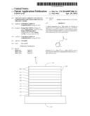
[0007] FIG. 1 shows the structure of an OLED according to an embodiment of the present invention.
[0008] FIG. 2 shows a plot of the luminous efficiency of an experimental and comparative device.
[0009] FIG. 3 shows the operating lifetime of an experimental and comparative device depicted as a plot of luminous intensity over time.
DETAILED DESCRIPTION
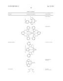
[0010] The present invention relates to the forming of organic layers by solution processing techniques. In one aspect, the present invention provides a liquid composition which can be used for forming an organic layer by solution processing techniques. The liquid composition comprises a small molecule organic semiconductor material mixed in a solvent in which the solvent compound has the following formula:
##STR00003##
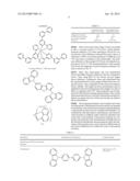
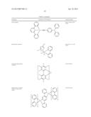
wherein R1 is C1-6 alkyl; R2 is C1-6 alkyl; and R3 is one or more optional substitutions independently selected from C1-6 alkyl and lower aryl. The term "alkyl" means alkyl moieties and encompasses both straight and branched alkyl chains, such as methyl, ethyl, propyl, isopropyl, butyl, isobutyl, tert-butyl, and the like. The term "aryl" means a hydrocarbyl containing at least one aromatic ring, such as substituted phenyl. The term "lower aryl" means an aryl containing from 3-15 carbon atoms. Representative examples of solvents having this formula include the following:
##STR00004##
[0011] Methyl phenoxyacetate (BP ˜245° C.) Ethyl phenoxyacetate (BP ˜247° C.)
[0012] The solvent used in the present invention may have various chemical/physical properties that make it useful for forming organic layers by solution processing techniques, such as inkjet printing. For example, the solvent may have a melting point of 25° C. or lower. In some cases, the solvent compound has a molecular weight in the range of 166-400. In some cases, the solvent has a boiling point of 260° C. or lower at 1 atm; and in some cases, in the range of 150-260° C. at 1 atm, but other boiling point ranges are also possible. Boiling points in this range may be sufficiently high to prevent nozzle clogging of an inkjet print head, but sufficiently low to allow removal by drying/baking during device fabrication.
[0013] The organic semiconductor material is a small molecule organic compound (including organometallic compounds) which is capable of exhibiting semiconducting properties, i.e., in which the energy gap between conduction and valence bands is in the range of 0.1-4 eV. The small molecule organic semiconductor material may be any of those known or proposed to be used in the fabrication of organic electronic devices, such as organic light emitting devices. For example, the organic semiconductor material may be a charge transport compound (hole or electron transporting, or hole or electron injecting) or an emissive phosphorescent compound.
[0014] The term "small molecule" refers to any compound that is not a polymer, and "small molecules" may actually be relatively large. Small molecules may include repeat units in some circumstances. For example, using a long chain alkyl group as a substituent does not exclude the molecule from being a "small molecule." In general, a small molecule has a well-defined chemical formula with a single molecular weight, whereas a polymer has a chemical formula and a molecular weight that may vary from molecule to molecule. The molecular weight of the small molecule organic semiconductor material is typically 3,000 or less.
[0015] In some cases, the organic semiconductor material is a phosphorescent emitting compound. Any of various types of phosphorescent emitting compounds may be suitable, including the organometallic complexes of transition metals described in U.S. Pat. No. 6,902,830 (Thompson et. al.); and U.S. Published Appln. No. 2006/0251923 (Lin et al.), No. 2007/0088167 (Lin et al.), No. 2006/0008673 (Kwong et al.), and No. 2007/0003789 (Kwong et al.), all of which are incorporated by reference herein.
[0016] The concentration of the organic semiconductor material in the liquid composition will vary according to the particular application. In certain embodiments, the organic semiconductor material is provided at a concentration that is suitable for inkjet printing. In some cases, the concentration of the organic semiconductor material is in the range of 0.01-10 wt %; and in some cases, in the range of 0.01-2 wt %; and in some cases, in the range of 0.1-1 wt %. The viscosity of the liquid composition will vary according to the particular application. For use in inkjet printing, an appropriate viscosity for the liquid composition can be in the range of 5-15 cPs or 7-12 cPs at 23° C. For liquid compositions of small molecule materials, the solvent viscosity may be the major contributor of the viscosity of the liquid composition. As such, in some cases, the viscosity of the solvent used in the liquid composition can be in the range of 5-15 cPs or 7-12 cPs at 23° C. In some cases, the solvent has a lower boiling point than 3-phenoxytoluene and a higher viscosity than 3-phenoxytoluene.
[0017] The interaction of the solvent with the organic semiconductor material may affect the viscosity of the liquid composition. As such, the viscosity of the liquid composition may be adjusted by varying the selection of the solvent and/or the organic semiconductor material, or by varying the relative amounts of each. The liquid composition may also contain any of various other types of materials used in the fabrication of organic electronic devices, such as OLEDs. The organic layer may be any of those used in OLEDs (e.g., an emissive layer, a hole injection layer, or a hole transporting layer in an OLED).
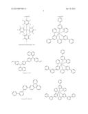
[0018] In cases where the liquid composition is used to make an emissive layer of an OLED, in some cases, the liquid composition may include a small molecule host compound and a small molecule phosphorescent emitting compound as a dopant in the emissive layer. A host is a compound in the emissive layer that functions as the component which receives the hole/electron recombination energy and then by an emission/absorption energy transfer process, transfers that excitation energy to the phosphorescent dopant compound. The phosphorescent dopant is typically present in lower concentrations than the host compound. Examples of host compounds include Alq3 [aluminum(III)tris(8-hydroxyquinoline)], mCP (1,3-N,N-dicarbazole-benzene), and CBP (4,4'-N,N-dicarbazole-biphenyl). Other materials that may be used as phosphorescent emitting compounds or host compounds are shown in Table 2 below.
[0019] The liquid composition is deposited onto the surface using any suitable solution processing technique known in the art. For example, the liquid composition can be deposited using a printing process, such as inkjet printing, nozzle printing, offset printing, transfer printing, or screen printing; or for example, using a coating process, such as spray coating, spin coating, or dip coating. After deposition of the liquid composition, the solvent is removed, which may be performed using any conventional method such as vacuum drying or heating.
[0020] In some cases, the liquid composition may have a blend of solvents. For example, the liquid composition may further include the solvents disclosed in U.S. Pat. No. 8,174,000 or those that are not solvents of the present invention. In such cases, the solvent(s) of the present invention constitutes at least 10% (by volume) of the solvent volume in the liquid composition. Such blended solvents can enhance film formation and/or reduce defects in the deposited organic layer. This second solvent can have various properties to complement those of the aryloxy-alkylcarboxylate solvent of the present invention, such as having a higher or lower boiling point or having a higher degree of interaction with the organic semiconductor material than the aryloxy-alkylcarboxylate solvent. An example of a solvent that can be used for blending is 3-phenoxytoluene, which has a relatively high boiling point and a relatively lower viscosity. As such, blending with 3-phenoxytoluene can be used to raise the boiling point or reduce the viscosity of the liquid composition.
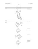
[0021] The present invention can be used in the fabrication of a variety of organic electronic devices, including organic light emitting devices, organic field-effect transistors (OFETs), organic thin-film transistors (OTFTs), organic photovoltaic devices, and organic solar cells, such as those disclosed in U.S. Appln. Publication No. 2005/0072021 (Steiger et al.), which is incorporated by reference herein. For example, FIG. 1 shows an OLED 100 that may be made using the present invention. OLED 100 has an architecture that is well-known in the art (see, for example, U.S. Appln. Publication No. 2008/0220265 to Xia et al., which is incorporated by reference herein). As seen in FIG. 1, OLED 100 has a substrate 110, an anode 115, a hole injection layer 120 (HIL), a hole transport layer 125 (HTL), an electron blocking layer 130 (EBL), an emissive layer 135 (EML), a hole blocking layer 140 (HBL), an electron transport layer 145 (ETL), an electron injection layer 150 (EIL), a protective layer 155, and a cathode 160. Cathode 160 is a compound cathode having a first conductive layer 162 and a second conductive layer 164. Examples of dopants or hosts that can be used in the emissive layer are given in Table 2 below.
[0022] Where a first layer is described as being "over" a second layer, the first layer is positioned further away from substrate. There may be other layers between the first and second layer, unless it is specified that the first layer is "in physical contact with" the second layer. For example, a cathode may be described as being disposed "over" an anode, even though there are various organic layers in between.
EXAMPLES
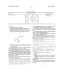
[0023] Specific representative embodiments of the invention will now be described, including how such embodiments may be made. The specific methods, materials, conditions, process parameters, apparatus, and the like, do not necessarily limit the scope of the invention.
[0024] An experimental and a comparative device were made with the following sequentially deposited organic layers: HIL/HTL/EML/HBL/ETL. The hole injection layer was deposited by inkjet printing onto a 1200 Å thick ITO (indium tin oxide) anode using a mixture of Compound A and Compound B (in an 80:20 weight ratio) in tetralone solvent at 0.15 wt % concentration. The hole transport layer was deposited by inkjet printing onto the hole injection layer using 0.2 wt % of Compound C in 3-phenoxytoluene (3-PT) solvent. For the experimental device, the emissive layer was deposited by inkjet printing using Compound D:Compound Mixture E (88:12 ratio) in methyl phenoxyacetate (MPA) solvent at a concentration of 0.85%. For the comparative device, 3-phenoxytoluene (3-PT) was used as the solvent instead of MPA. MPA has a boiling point of ˜245° C. and a viscosity of ˜9 cPs at 23° C.; whereas 3-PT has a boiling point of ˜275° C. and a viscosity of ˜4.8 cPs at 23° C.
[0025] These inkjet-deposited layers were prepared in a nitrogen glove box with stirring to ensure complete dissolution of the materials. Deposition of the inkjet solutions was followed by immediate vacuum drying and baking: 250° C. for 30 mins. for the HIL; 200° C. for 30 mins. for the HTL; 100° C. for 60 mins. for the EML. A blocking layer containing Compound F, an electron transport layer containing Alq3 [aluminum(III)tris(8 hydroxyquinoline)], and 10 Å LiF/1,000 Å of aluminum for the cathode were sequentially deposited by vacuum thermal evaporation in a conventional fashion. Immediately after fabrication, all devices were encapsulated with a glass lid sealed with an epoxy resin in a nitrogen glove box (1 ppm of H2O and O2), and a moisture getter was incorporated inside the package.
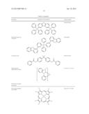
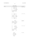
##STR00005## ##STR00006## ##STR00007##
TABLE-US-00001 TABLE 1 Comparative device Experimental device (using 3-PT solvent) (using MPA solvent) Voltage @ 10 mA/cm2 8.2 7.6 LE (cd/A) @ 10 mA/cm2 38.8 46.4 LT80 (hours) @ 4k nits 123 162 CIE (x, y) (0.34, 0.62) (0.32, 0.63)
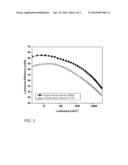
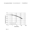
[0026] Table 1 above shows the voltage (V) that was needed to drive a constant current of 10 mA/cm2 current density; luminous efficiency (LE) when operating at 10 mA/cm2 current density; device lifetime as measured by time to decay of luminance to 80% of an initial luminance of 4,000 nits; and CIE color space coordinates of the emitted light. The luminous efficiency of the example OLEDs are also depicted as a plot shown in FIG. 2. The operating lifetimes of the example OLEDs are also depicted as a plot of luminous intensity over time as shown in FIG. 3.
[0027] These data demonstrate that the experimental device had higher luminous efficiency than the comparative device. Thus, using MPA for the solvent can give higher device efficiency. Furthermore, these data demonstrate that the experimental device had a longer lifetime than the comparative device. Thus, using MPA for the solvent can improve device stability. This improved device performance may be attributed to the lower boiling point and/or higher viscosity of MPA as compared with 3-PT. These properties may be beneficial for film formation during inkjet printing. These results demonstrate that the use of solvents of the present invention to deposit an organic layer by solution processing can enhance device performance.
[0028] The foregoing description and examples have been set forth merely to illustrate the invention and are not intended to be limiting. Each of the disclosed aspects and embodiments of the present invention may be considered individually or in combination with other aspects, embodiments, and variations of the invention. In addition, unless otherwise specified, none of the steps of the methods of the present invention are confined to any particular order of performance. Modifications of the disclosed embodiments incorporating the spirit and substance of the invention may occur to persons skilled in the art and such modifications are within the scope of the present invention.
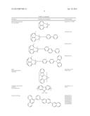
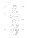
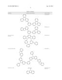
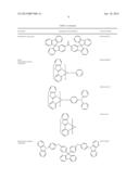
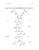
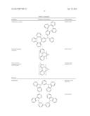
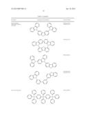
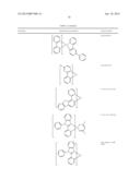
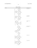
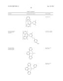
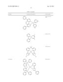
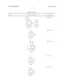
TABLE-US-00002 TABLE 2 MATERIAL EXAMPLES OF MATERIAL PUBLICATIONS Phosphorescent OLED host materials Red hosts Arylcarbazoles ##STR00008## Appl. Phys. Lett. 78, 1622 (2001) Metal 8-hydroxyquinolates (e.g., Alq3, BAlq) ##STR00009## Nature 395, 151 (1998) ##STR00010## US20060202194 ##STR00011## WO2005014551 ##STR00012## WO2006072002 Metal phenoxybenzothiazole compounds ##STR00013## Appl. Phys. Lett. 90, 123509 (2007) Conjugated oligomers and polymers (e.g., polyfluorene) ##STR00014## Org. Electron. 1, 15 (2000) Aromatic fused rings ##STR00015## WO2009066779, WO2009066778, WO2009063833, US20090045731, US20090045730, WO2009008311, US20090008605, US20090009065 Zinc complexes ##STR00016## WO2009062578 Green hosts Arylcarbazoles ##STR00017## Appl. Phys. Lett. 78, 1622 (2001) ##STR00018## US20030175553 ##STR00019## WO2001039234 Aryltriphenylene compounds ##STR00020## US20060280965 ##STR00021## US20060280965 ##STR00022## WO2009021126 Donor acceptor type molecules ##STR00023## WO2008056746 Aza-carbazole/DBT/DBF ##STR00024## JP2008074939 Polymers (e.g., PVK) ##STR00025## Appl. Phys. Lett. 77, 2280 (2000) Spirofluorene compounds ##STR00026## WO2004093207 Metal phenoxybenzooxazole compounds ##STR00027## WO2005089025 ##STR00028## WO2006132173 ##STR00029## JP200511610 Spirofluorene-carbazole compounds ##STR00030## JP2007254297 ##STR00031## JP2007254297 Indolocabazoles ##STR00032## WO2007063796 ##STR00033## WO2007063754 5-member ring electron deficient heterocycles (e.g., triazole, oxadiazole) ##STR00034## J. Appl. Phys. 90, 5048 (2001) ##STR00035## WO2004107822 Tetraphenylene complexes ##STR00036## US20050112407 Metal phenoxypyridine compounds ##STR00037## WO2005030900 Metal coordination complexes (e.g., Zn, Al with N{circumflex over ( )}N ligands) ##STR00038## US20040137268, US20040137267 Blue hosts Arylcarbazoles ##STR00039## Appl. Phys. Lett, 82, 2422 (2003) ##STR00040## US20070190359 Dibenzothiophene/ Dibenzofuran-carbazole compounds ##STR00041## WO2006114966, US20090167162 ##STR00042## US20090167162 ##STR00043## WO2009086028 ##STR00044## US20090030202, US20090017330 Silicon aryl compounds ##STR00045## US20050238919 ##STR00046## WO2009003898 Silicon/Germanium aryl compounds ##STR00047## EP2034538A Aryl benzoyl ester ##STR00048## WO2006100298 High triplet metal organometallic complex ##STR00049## U.S. Pat. No. 7,154,114 Phosphorescent dopants Red dopants Heavy metal porphyrins (e.g., PtOEP) ##STR00050## Nature 395, 151 (1998) Iridium(III) organometallic complexes ##STR00051## Appl. Phys. Lett. 78, 1622 (2001) ##STR00052## US2006835469 ##STR00053## US2006835469 ##STR00054## US20060202194 ##STR00055## US20060202194 ##STR00056## US20070087321 ##STR00057## US20070087321 ##STR00058## Adv. Mater. 19, 739 (2007) ##STR00059## WO2009100991 ##STR00060## WO2008101842 Platinum(II) organometallic complexes ##STR00061## WO2003040257 Osminum(III) complexes ##STR00062## Chem. Mater. 17, 3532 (2005) Ruthenium(II) complexes ##STR00063## Adv. Mater. 17, 1059 (2005) Rhenium (I), (II), and (III) complexes ##STR00064## US20050244673 Green dopants Iridium(III) organometallic complexes ##STR00065## Inorg. Chem. 40, 1704 (2001) ##STR00066## US20020034656 ##STR00067## U.S. Pat. No. 7,332,232 ##STR00068## US20090108737 ##STR00069## US20090039776 ##STR00070## U.S. Pat. No. 6,921,915 ##STR00071## U.S. Pat. No. 6,687,266 ##STR00072## Chem. Mater. 16, 2480 (2004) ##STR00073## US20070190359 ##STR00074## US 20060008670 JP2007123392 ##STR00075## Adv. Mater. 16, 2003 (2004) ##STR00076## Angew. Chem. Int. Ed. 2006, 45, 7800 ##STR00077## WO2009050290 ##STR00078## US20090165846 ##STR00079## US20080015355 Monomer for polymeric metal organometallic compounds ##STR00080## U.S. Pat. No. 7,250,226, U.S. Pat. No. 7,396,598 Pt(II) organometallic complexes, including polydentated ligands ##STR00081## Appl. Phys. Lett. 86, 153505 (2005) ##STR00082## Appl. Phys. Lett. 86, 153505 (2005) ##STR00083## Chem. Lett. 34, 592 (2005) ##STR00084## WO2002015645 ##STR00085## US20060263635 Cu complexes ##STR00086## WO2009000673 Gold complexes ##STR00087## Chem. Commun. 2906 (2005) Rhenium(III) complexes ##STR00088## Inorg. Chem. 42, 1248 (2003) Deuterated organometallic complexes ##STR00089## US20030138657 Organometallic complexes with two or more metal centers ##STR00090## US20030152802 ##STR00091## U.S. Pat. No. 7,090,928 Blue dopants Iridium(III) organometallic complexes ##STR00092## WO2002002714 ##STR00093## WO2006009024 ##STR00094## US20060251923 ##STR00095## U.S. Pat. No. 7,393,599, WO2006056418, US20050260441, WO2005019373 ##STR00096## U.S. Pat. No. 7,534,505 ##STR00097## U.S. Pat. No. 7,445,855 ##STR00098## US20070190359, US20080297033 ##STR00099## U.S. Pat. No. 7,338,722 ##STR00100## US20020134984 ##STR00101## Angew. Chem. Int. Ed. 47, 1 (2008) ##STR00102## Chem. Mater. 18, 5119 (2006) ##STR00103## Inorg. Chem. 46, 4308 (2007) ##STR00104## WO2005123873 ##STR00105## WO2005123873 ##STR00106## WO2007004380 ##STR00107## WO2006082742 Osmium(II) complexes ##STR00108## U.S. Pat. No. 7,279,704 ##STR00109## Organometallics 23, 3745 (2004) Gold complexes ##STR00110## Appl. Phys. Lett. 74, 1361 (1999) Platinum(II) complexes ##STR00111## WO2006098120, WO2006103874
User Contributions:
Comment about this patent or add new information about this topic:
| People who visited this patent also read: | |
| Patent application number | Title |
|---|---|
| 20170073817 | NANOMETAL-NANOCARBON HYBRID MATERIAL AND METHOD OF MANUFACTURING THE SAME |
| 20170073816 | CHROME-FREE ADHESION PRE-TREATMENT FOR PLASTICS |
| 20170073815 | METHOD FOR A NON-AQUEOUS ELECTROLESS POLYOL DEPOSITION OF METAL OR METAL ALLOY IN FEATURES OF A SUBSTRATE |
| 20170073814 | NANOFABRICATION USING A NEW CLASS OF ELECTRON BEAM INDUCED SURFACE PROCESSING TECHNIQUES |
| 20170073813 | SUBSTRATE PROCESSING APPARATUS |
Images included with this patent application:
 |  |
 |  |
 |  |
 |  |
 |  |
 |  |
 |  |
 |  |
 |  |
 |  |
 |  |
 |  |
 |  |
 |  |
 |  |
| Similar patent applications: | |
| Date | Title |
|---|---|
| 2014-01-30 | Star-shaped compounds for organic solar cells |
| 2014-02-27 | Stacked microelectronic packages having sidewall conductors and methods for the fabrication thereof |
| 2010-09-02 | Deposition of organic layers |
| 2014-02-27 | Isolation structures for finfet semiconductor devices |
| 2012-07-12 | Method for direct deposition of a germanium layer |
| New patent applications in this class: | |
| Date | Title |
|---|---|
| 2022-05-05 | Display device |
| 2022-05-05 | Display device and manufacturing method thereof |
| 2022-05-05 | Photoelectric conversion element, organic photoconductor, image forming method, image forming apparatus, and organic el element |
| 2022-05-05 | Display substrate, preparation method thereof, and display device |
| 2022-05-05 | Display device and electronic apparatus |
| New patent applications from these inventors: | |
| Date | Title |
|---|---|
| 2022-09-01 | Organic electroluminescent materials and devices |
| 2022-07-21 | Organic electroluminescent materials and devices |
| 2019-10-17 | Host materials for electroluminescent devices |
| 2019-09-12 | Metal complex for phosphorescent oled |
| 2016-01-28 | Organic electroluminescent materials and devices |
| Top Inventors for class "Active solid-state devices (e.g., transistors, solid-state diodes)" | |
| Rank | Inventor's name |
|---|---|
| 1 | Shunpei Yamazaki |
| 2 | Shunpei Yamazaki |
| 3 | Kangguo Cheng |
| 4 | Huilong Zhu |
| 5 | Chen-Hua Yu |