Patent application title: ARRANGEMENT FOR ELECTRICALLY CONDUCTIVELY CONNECTING TWO SUPERCONDUCTIVE CONDUCTORS
Inventors:
Rainer Soika (Hannover, DE)
Rainer Soika (Hannover, DE)
Mark Stemmle (Hannover, DE)
Mark Stemmle (Hannover, DE)
IPC8 Class: AH01B1202FI
USPC Class:
505230
Class name: Superconductor technology: apparatus, material, process high temperature (tc greater than 30 k) devices, systems, apparatus, com- ponents, or stock, or processes of using superconducting wire, tape, cable, or fiber, per se
Publication date: 2014-03-20
Patent application number: 20140080713
Abstract:
An arrangement for electrically conductively connecting two
superconductive strip-shaped electrical conductors (1, 2) having at least
approximately the same width, where the two conductors (1, 2) rest
against each other with their end faces against each other in a
connecting point (V). A strip (6) of superconductive material is soldered
to the two conductors (1, 2), where the strip extends beyond both
conductors so as to cover the connecting point (V). A strip (6) is used
which has, only in the area of the connecting point (V) between the two
conductors (1, 2), at least approximately the same width as the
conductors, and where the strip narrows on both sides of the connecting
point (V) and facing away from the connecting point (V).Claims:
1. Arrangement for electrically conductively connecting two
superconductive strip-shaped electric lines having approximately the same
width, where the two conductors rest against each other with their end
faces in a connecting point, and where a strip of superconductive
material is soldered to both conductors, where the strip extends beyond
both conductors so as to cover the connecting point, said arrangement
comprises: said strip of superconductive material has, only in the area
of the connecting point between the two conductors, at least
approximately the same width as conductors, and that on both sides of the
connecting point the strip narrows facing away from the connecting point.
2. Arrangement according to claim 1, wherein the ends of the strip are rounded.
3. Arrangement according to claim 1, wherein the strip symmetrically narrows preferably in accordance with a conical pattern relative to the center line of the conductors.
4. Arrangement according to claim 1, wherein the strip is constructed thinner in its border areas than in its central area located in the area of the center line of the conductors.
5. Arrangement according to claim 4, wherein the strip is constructed thinner in its border areas than in its central area located in the area of the center line of the conductors, with continuous transition between its border areas and its central area.
Description:
RELATED APPLICATION
[0001] This application claims the benefit of priority from European Patent Application. No. 12 306 106.1, filed on Sep. 14, 2012, the entirety of which is incorporated by reference.
BACKGROUND
[0002] 1. Field of the Invention
[0003] The invention relates to an arrangement for electrically conductively connecting two superconductive strip-shaped electrical conductors having at least approximately the same width, wherein the two conductors rest against each other with their end faces at a connecting point, and wherein a strip of superconductive material is soldered to both conductors which extends over both conductors so as to cover the connecting point. (Publication of American Company at AMSC from the year 2010, "Guidelines for and--Assembled Splicing of Amperium Wire," Pages 1 to 7).
[0004] 2. Description of Related Art
[0005] Materials suitable for superconductive conductors are, for example, oxidic materials on the basis of rare earths (ReBCO), particularly YBCO (yttrium-barium-copper oxide) or BSCCO (bismuth-strontium-calcium-copper oxide). Magnesium boride is also known as a superconductive material. Superconductive conductors of the mentioned materials can be manufactured with relatively great length. For manufacturing superconductive cables, the conductors are wound, for example, around a core or another substrate. A conductor having the appropriate length is required for a continuous manufacture of a superconductive cable. It may then be necessary that two or more lengths of the superconductive conductor must be electrically conductively connected to each other. Such a connection of two sections of a conductor must also be carried out when a damaged portion of the conductor has to be cut out, or when the conductor tears during the manufacture.
[0006] Arrangements of this type are disclosed in the above mentioned publication of the company AMSC for superconductive conductors, in which the superconductive material is mounted on a buffer layer which is, in turn, placed on a carrier layer. Consequently, two superconductive conductors can be connected to each other by turning one of the conductors about 180° and placing its superconductive layer onto the superconductive layer of the other conductor. The two conductors are then soldered together. Another possibility is to position the two conductors with their end faces against each other and to solder a rectangular strip of superconductive material onto the two conductors, wherein the strip has at least approximately the same width as the two conductors. In both cases the connecting point between the two conductors is relatively stiff, so that the bending capability of the conductor is negatively affected.
[0007] 3. Objects and Summary
[0008] The invention is based on the object of configuring the above described. arrangement in such a way that the bending capability of the superconductive conductor at the connecting points is improved.
[0009] In accordance with the invention, this object is met in that a strip is used which has approximately the same width as the conductors only in the region of the connecting point between the two conductors, and becomes narrower on both sides of the connecting point facing away from the connecting point.
[0010] The two conductors are sufficiently tightly connected at their connecting point by the strip because the strip has approximately the same width as the conductors in the area of the connecting point. The bending capability of the single-piece conductor manufactured with the strip is significantly improved by the narrowing of the strip on both sides of the connecting point because due to the narrowing less material may have to be bent. Since with increasing distance from the connecting point the strip has an increasing distance from the side edges of the two conductors which are connected to each other and the danger of damage to the layers shaped around the conductor is additionally reduced, for example, during the manufacture of a superconductive cable.
[0011] Particularly advantageously the strip narrows with a conical pattern symmetrically relative to the center line of the conductor. Its ends are preferably rounded. The border areas of the strip are additionally constructed thinner than the central portion.
BRIEF DESCRIPTION OF THE DRAWINGS
[0012] An embodiment of the subject matter of the invention is illustrated in the drawings.
[0013] In the drawing:
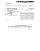
[0014] FIG. 1 is a side view of the arrangement according to the invention, in a schematic sectional view.
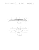
[0015] FIG. 2 is a top view of the arrangement according to FIG. 1.
DETAILED DESCRIPTION
[0016] The following description refers also to conductors of all other superconductive materials of the so-called second generation. with, for example, YBCO as the superconductive material representative of all these other superconductive materials. This material according to the above mentioned publication of the company AMSC is applied, for example, onto a substructure which is composed of at least a carrier layer and a buffer layer placed on the carrier layer. The superconductive material is applied to the buffer layer. It may additionally be covered by a thin protective layer of electrically conducting material such as silver. A further electrically conducting layer may be mounted above this layer which is composed, for example, of copper.
[0017] FIG. 1 shows a connecting point V between two superconductive strip-shaped conductors 1 and 2. The two conductors 1 and 2 should have at least approximately the same width. Each of the two conductors 1 and 2 has a carrier layer 3 which may be, for example, a biaxially textured strip of nickel, copper or iron. A buffer layer 4 each is applied to the carrier laver, wherein the buffer layer 4 may be of copper or silver. The layer 5 placed on the buffer layer 4 is of a superconductive material, for example YBCO. As already mentioned, an additional electrically conductive protective layer and another layer which is also electrically conductive may be mounted above the layer 5.
[0018] The two conductors 1 and 2 are fixedly connected to each other through a strip 6 of superconductive material. For this purpose, the strip 6, whose configuration can be seen for example in FIG. 2, is soldered to the two conductors 1 and 2. Basically, it may be of the same construction as the two conductors 1 and 2 to be connected to each other. However, a differently constructed strip 6 of any chosen superconductive material may be used.
[0019] In the illustrated embodiment according to FIG. 2, the strip 6 has, in the area of the connecting point V, the same width as the conductors 1 and 2. At this location the strip should have at least approximately the same width as the conductors 1 and 2. Facing away from the connecting point V, the strip 6 is narrowed on both sides, specifically with a conical pattern advantageously symmetrical relative to the center line M of the two conductors 1 and 2. In a preferred embodiment the strip 6 is rounded at both ends as illustrated in the drawing. The strip 6 may additionally be constructed thinner in its border regions, preferably with a continuous transition, than in its central area which in the assembled state is located in the center line M of the two conductors 1 and 2. In this case, the thin border areas extend up into the "peaks" of the narrowing areas which are also thinner as a result.
User Contributions:
Comment about this patent or add new information about this topic:
Images included with this patent application:
 |  |
| Similar patent applications: | |
| Date | Title |
|---|---|
| 2014-03-27 | Efficient polarization independent single photon detector |
| 2014-06-05 | System and apparatus for compensating for magnetic field distortion in an mri system |
| 2014-06-05 | Oxide superconductor wire and superconducting coil |
| 2014-02-27 | Nmr rf probe coil exhibiting double resonance |
| 2014-06-05 | Nbti superconductor with reduced weight |
| New patent applications in this class: | |
| Date | Title |
|---|---|
| 2016-06-16 | Superconductor with improved flux pinning at low temperatures |
| 2016-06-09 | Methods and systems for preparing superconductors for reaction and integration |
| 2016-06-09 | Integrated superconductor device and method of fabrication |
| 2016-06-02 | Superconducting article with compliant layers |
| 2016-05-19 | Fins and foams heat exchangers with phase change for cryogenic thermal energy storage and fault current limiters |
| New patent applications from these inventors: | |
| Date | Title |
|---|---|
| 2017-01-26 | Arrangement for current limitation which is suitable for integration into a power supply serving network |
| 2016-03-10 | End closure of a superconductive electric cable |
| 2016-02-11 | Flexible pipeline |
| 2016-01-28 | Method of transmitting electrical energy |
| 2015-12-24 | Method and arrangement for constructing a superconductive cable system |
| Top Inventors for class "Superconductor technology: apparatus, material, process" | |
| Rank | Inventor's name |
|---|---|
| 1 | Mark Stemmle |
| 2 | Rainer Soika |
| 3 | Alexander Usoskin |
| 4 | Teruo Izumi |
| 5 | Douglas J. Gilbert |