Patent application title: CONNECTING COMPONENT EQUIPPED WITH HOLLOW INSERTS
Inventors:
Francois Marion (Saint Martin Le Vinoux, FR)
Assignees:
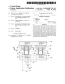
COMMISSARIAT A L'ENERGIE ATOMIQUE ET AUX ENERGIES ALTERNATIVES
IPC8 Class: AH05K310FI
USPC Class:
29825
Class name: Method of mechanical manufacture electrical device making conductor or circuit manufacturing
Publication date: 2014-03-20
Patent application number: 20140075747
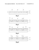
Abstract:
Electro-mechanical connection component provided on one connection
surface with conductive inserts intended to be inserted at ambient
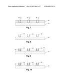
temperature into respective ductile conductive pads formed on a surface
of another connection component for a face-to-face type hybridization.
Each insert of the component includes: a hollow metal core formed of a
bottom arranged on the connection surface and of a lateral wall
protruding from said bottom, defining an internal surface of the insert,
at least a portion of said internal surface being non-oxidized; and a
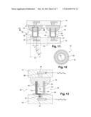
metal layer substantially only covering the internal surface of the metal
core.Claims:
1. A method of manufacturing an electro-mechanical connection component
provided on one connection surface with conductive inserts intended to be
inserted at ambient temperature into respective ductile conductive pads
formed on a surface of another connection component for a face-to-face
type hybridization, wherein the method comprises, for each insert:
forming a hollow metal core formed of a bottom arranged on the connection
surface and of a lateral wall protruding from said bottom, defining an
internal surface of the insert, at least a portion of said internal
surface being non-oxidized; and forming a metal layer substantially only
covering the internal surface of the metal core and intended to be in
contact with the pad associated with the insert; and wherein the metal
layer is made of an inoxidizable metal, especially a noble metal, or
wherein the forming of the metal layer comprises: forming a first metal
sub-layer non-oxidized over at least a portion of its surface, covering
at least said non-oxidized portion of the internal surface of the core,
the first sub-layer having a greater plasticity than the core; and
fouling a second sub-layer covering at least the first sub-layer over its
non-oxidized portion and having a lower plasticity than the first
sub-layer.
2. The method of claim 1, wherein the first sub-layer is made of an oxidizable metal and wherein the second sub-layer is made by oxidizing the first sub-layer to create a layer of native oxide of the metal forming the first sub-layer having a plasticity lower than that of the first sub-layer.
3. The method of claim 2, wherein the first sub-layer is made of aluminum, the second sub-layer being an aluminum oxide.
4. The method of claim 1, wherein the hollow metal core is made of a hard metal, particularly of titanium nitride, of tungsten nitride, of copper, of vanadium, of molybdenum, of nickel, of titanium tungstenate, of WSi, and/or of tungsten.
5. The method of claim 1, wherein the adherence of the second sub-layer to the first sub-layer is low so that the second sub-layer slides on the first sub-layer under the effect of a shearing applied to the stack of the first and second sub-layers.
6. The method of claim 1, wherein the first sub-layer has a ductility substantially equal to that of the pads.
7. A method of face-to-face type hybridization of a microelectronic component obtained according to the method of any of the foregoing claims with a micro-electronic component having on one of its surfaces respective ductile conductive pads having a lower hardness than the metal core of the hollow inserts, comprising the insertion at ambient temperature of the inserts, provided with their second metal sub-layer, into the pads.
8. The method of claim 7, wherein the interconnect pitch between microcomponents is smaller than 10 micrometers.
Description:
FIELD OF THE INVENTION
[0001] The invention relates to the connection of two components according to the flip-chip technique, and more specifically to the connection of two electronic components by insertion at ambient temperature of metal-type inserts in a metal forming pads.
[0002] The invention thus specifically applies in so-called chip-on-chip, chip-on-wafer, and wafer-on-wafer assemblies.
STATE OF THE ART
[0003] To replace flip-chip hybridizations with solder balls, it is known to provide on a surface of a first electronic component inserts made of a hard metal, for example, titanium nitride, and on a surface of a second electronic components, pads made of a ductile metal, for example, silver, and then to hybridize the two components by inserting at low temperature the inserts into the pads, which thus creates mechanical and electrical interconnects between components.
[0004] FIGS. 1 and 2 schematically illustrate the flip-chip hybridization of a first and of a second microelectronic components 10, 12. First component 10 comprises on one or its surface 14 a set of electrically-conductive inserts 16, intended to penetrate into respective electrically-conductive pads 18, pads 18 being arranged on surface 20 of second component 12.
[0005] The bottom of each insert 16 is further in contact with a connection area 22 formed in the thickness of first component 10, area 22 forming the interface with, for example, an electronic circuit 24. Similarly, each pad 18 is in contact with a connection area 26 formed in the thickness of second component 12, area 26 forming the interface, for example, with an electronic circuit 28.
[0006] To perform the hybridizing, preferably at cold temperature, electronic components 10 and 12 are aligned to present each insert 16 in front of a pad 18, and an appropriate pressure, illustrated by the arrows, is for example exerted on the first component, which is mobile (FIG. 1). Inserts 16, which have a greater hardness than pads 18, then penetrate into them. Interconnects 30 between first and second microelectronic components 10, 12 are thus formed (FIG. 2). Interconnects 30 mechanically fasten components 10, 12 together, while creating electric connections therebetween.
[0007] As an example, first component 10 is a detection matrix formed of a plurality of sensitive detection elements, especially for detecting electromagnetic radiation, and second component 12 is a circuit for reading said sensitive elements. Interconnects 30 thus form the electric connection of the read circuit with each of the sensitive elements of first component 10.
[0008] However, a recurrent problem in this type of hybridizing by metal-in-metal insertion lies in the fact that, with no specific operation, the insert surface oxidizes, which creates electric connections of poor quality between inserts and the pads into which they are inserted. Indeed, metals adapted for a cold insertion, more commonly "hard" metals, such as for example titanium nitride, are oxidizable.
[0009] A solution used to avoid the insertion of oxidized inserts is to manufacture inserts 16, each formed of a central metal core having a greater hardness than pads 18, and to cover this core, before its oxidation, with a layer of a noble metal, which is thus non-oxidizable, such as gold or platinum. The core and the layer of noble metal are thus inserted together into a pad 18 without for oxide capable of affecting the quality of the electric connection to appear.
[0010] An example of a method of low cost manufacturing of hollow cylindrical inserts 16 covered with a layer of noble metal is described hereafter in relation with the simplified cross-section views of FIGS. 3 to 10.
[0011] The method starts with the deposition of a sacrificial layer 40 having a thickness e on surface 14 of component 10, for example, a polyimide-type resin layer, followed by a photolithography to form circular holes 42 in sacrificial layer 40 all the way to surface 14 of component 10 (FIG. 3). Thickness e corresponds to the height desired for the insert core and the diameter of circular holes 42 corresponds to the outer diameter of the core.
[0012] The method carries on with the full-plate deposition of a layer or a multilayer of hard metal 44, for example, titanium nitride or an alloy containing titanium nitride, of a thickness corresponding to the thickness of the core of inserts 16. The deposition is for example a chemical vapor deposition, or CVD, performed at a temperature compatible with the microelectronic elements of component 10, especially a temperature lower than 425° C. for a component 10 implementing a CMOS technology (FIG. 4).
[0013] A removal of the portion of hard metal 44 deposited between holes 42 is then performed, for example, by means of a damascene or gap fill etching, well known per se.
[0014] For example, according to the gap-fill etching, a full-plate deposition of fluid resin layer 46 is performed, said layer thus filling holes 42 and planarizing the assembly obtained at the previous step (FIG. 5). Once solidified, resin layer 46 is then uniformly etched, for example, by mechanical or chem.-mech. polishing, until metal layer surface 46 is reached. Holes 42 however remain filled with resin 46 to protect the metal covering them during subsequent steps (FIG. 6). An etching of metal 44 arranged between holes 42 is then implemented in a manner known per se (FIG. 7).
[0015] The method then carries on with the removal of resin 46 contained in holes 42, for example, by means of a decoating based on an O2 plasma, followed by the removal of sacrificial layer 40, for example, by means of a decoating based on an O2 plasma (FIG. 8). Cores 50 of inserts 16 are thus formed.
[0016] A layer 52 of noble metal, for example a gold or platinum layer, is then deposited full plate, for example, by means of a CVD (FIG. 9), after which the portion of layer 52 placed between cores 50 is removed, for example, by means of the conventional photolithography technique (FIG. 10).
[0017] However, this method has a number of disadvantages. First, even though the method has a low cost and provides a high manufacturing efficiency, it implements a large number of complex steps.
[0018] Then, this type of method makes it difficult or even impossible to decrease interconnect pitches, that is, the minimum space between two insert/pad interconnects, if low-cost techniques of manufacturing the noble metal layer covering the metal cores of the inserts are used. Indeed, low-cost manufacturing techniques comprise performing a full-plate deposition of a noble metal layer on the surface of the component comprising the inserts, and then etching the noble metal layer present between inserts. Now, the only low-cost etching technique of the state of the art applicable to noble metals such as gold and platinum is a liquid chemical etching which does not enable, to date, to etch surfaces having dimensions smaller than 10 micrometers, or even 15 micrometers. Only an ion machining etching currently enables to etch interconnect pitches smaller than 10 micrometers. However, such a technique has a very low efficiency, especially due to the cleanings required between each deposition, and it thus expensive.
[0019] This difficulty to decrease the interconnect pitch is illustrated in the simplified cross-section views of FIGS. 11 and 12.
[0020] Particularly, as can be seen in FIG. 11, noble metal layer 52 is not totally removed between inserts 16 due to the accuracy of the liquid etching used. A ring of noble metal 54 thus remains around each insert 16.
[0021] With the simplified assumption of cylindrical connection areas 22 aligned with their respective inserts 16, minimum interconnect pitch P is equal to the sum of width L1 of connection area 22, of twice width G1 between the external diameter of core 50 of an insert 16 and the edge of connection area 22, of twice width G2 between the external diameter of core 50 and the edge of ring 54 surrounding an insert 16, and of width L4 separating two rings 54 of adjacent inserts 16, that is, P=L1+2G1+2G2+L4.
[0022] Width L1 is mainly determined by the maximum current intended to cross interconnect 30 formed of an insert 16 inserted in a pad 18 and is thus substantially independent from the method of manufacturing inserts 16. A minimum width L1, for example, in imagers, is 3 micrometers.
[0023] Width G1 depends on the accuracy of the photolithography used to form openings 42 in sacrificial layer 40. By means of current etching techniques, the minimum possible width G1 is approximately 1 micrometer.
[0024] Width G2 depends on the accuracy of the photolithography used to remove noble metal layer 52 between inserts 16. By means of current etchings, the minimum possible width G2 is approximately 1 micrometer.
[0025] Finally, width L4 also represents the distance separating two adjacent conductive interconnect elements 30. It can be estimated that a minimum width L4 of approximately 3 micrometers is appropriate to avoid any risk of short-circuit between interconnects.
[0026] Further, noble metals, for example, gold or platinum, are highly reflective, which hinders the photolithographic etching. Further, etch chemistries are very aggressive for circuits, particularly image sensors.
[0027] Thus, the minimum interconnect pitch P which can currently be achieved is approximately 10 micrometers, that is, an interconnect surface density equal to approximately 104 interconnects/mm2.
BRIEF DESCRIPTION OF THE INVENTION
[0028] The present invention aims at providing inserts enabling to decrease the interconnect pitch and which can be achieved with current manufacturing techniques, as well as at a low-cost method of manufacturing such inserts, and particularly a method also enabling to perform a hybridization of microcomponents at ambient temperature.
[0029] For this purpose, an object of the invention is a method for manufacturing an electro-mechanical connection component provided on one connection surface with conductive inserts intended to be inserted at ambient temperature into respective ductile conductive pads formed on a surface of another connection component for a face-to-face type hybridization.
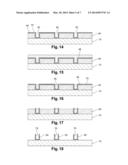
[0030] According to the invention:
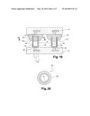
[0031] the method comprises, for each insert:
[0032] forming a hollow metal core formed of a bottom arranged on the connection surface and of a lateral wall protruding from said bottom, defining an internal surface of the insert, at least a portion of said internal surface being non-oxidized; and
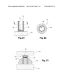
[0033] forming a metal layer substantially only covering the internal surface of the metal core and intended to be in contact with the pad associated with the insert;
[0034] and the metal layer is made of an inoxidizable metal, especially a noble metal, or the forming of the metal layer comprises:
[0035] forming a first metal sub-layer non-oxidized over at least a portion of its surface, covering at least said non-oxidized portion of the internal surface of the core, the first sub-layer having a greater plasticity than the core; and
[0036] forming a second sub-layer covering at least the first sub-layer over its non-oxidized portion and having a lower plasticity than the first sub-layer.
[0037] "Ambient temperature" here means a temperature remote from the melting temperature of the material forming the first layer and the pads, for example, temperatures on the order of 300° K for which no significant softening of this first layer and of the pads where the inserts are intended to be inserted can be observed. The "cold" or "ambient temperature" hybridization of the invention thus differs from "thermo-compressive"-type hybridizations during which both a pressure and a heating are applied, the heating aiming at softening or melting the pads in order to ease the insertion of inserts.
[0038] In other words, it is chosen not to totally cover the central metal core of inserts, but only its hollow portion, and thus to take no specific measure to avoid the oxidation of the external surface of the central core. Avoiding covering the external surface of the core with a layer of noble metal enables to do away with the presence of a ring of noble metal around the inserts.
[0039] Indeed, attempting to protect the entire oxidizable surface of the central core by implementing low-cost manufacturing methods, and particularly a full-plate deposition, results in depositing an unwanted metal layer between inserts, which unwanted layer then has to be removed by means of a low-cost etching of limited accuracy. Thus, metal rings are inevitably formed around the inserts, which limits the minimizing of the interconnect pitch.
[0040] It should be noted that as large a conductive surface area as possible has been desired up to now for an insert, in order to maximize the quality of the electric interconnect formed of an insert and of a pad. This, in particular, used to be the reason to totally cover the central conductive core with a layer of noble metal to avoid any oxidizing of the core surface. This thus implies, in the context of a low-cost manufacturing, disengaging the central core of the inserts from the sacrificial layer in which it is formed, to perform a full-plate deposition, to totally coat this core with a layer of noble metal.
[0041] However, the inventors have observed that this approach is actually based on a technically erroneous assumption, that is, that the external surface and the internal surface of the core define electric paths of similar importance.
[0042] Actually, noble metals, and more generally non-oxidizable metals, have a lower electric resistivity than the hard metals used to form the central core. Thus, the current preferably runs through the noble metal layer rather than through the central core.
[0043] Referring to the simplified cross-section view of FIG. 13, when a total current Itot flows through an interconnect 30, for example, a current injected via area 26 of pad 18, total current Itot breaks down into a first current Iint flowing in internal portion 60 of noble metal layer 52 and a second current iext flowing in external portion 62 of layer 52. Now, as can be seen, external current iext has to cross twice central core 50, which has a greater resistivity than layer 52, to reach connection area 22 of insert 16. However, internal current Iint only crosses the core once, at bottom 64 thereof. Measurements thus show that internal current Iint amounts to 90% of total current Itot and thus that external current iext only amounts to 10% of this current.
[0044] Thus, external portion 62 of noble metal layer 52 can be considered as a dead arm with a negligible electric conduction and its removal causes no substantial alteration of the electric conduction of an interconnect 30.
[0045] Further, according to a first variation, the metal layer being formed of an inoxidizable metal, particularly a noble metal such as gold or platinum, this enables to define a non-oxidized surface at the interface with the pad when the insert is inserted into the pad.
[0046] However, this variation has a number of disadvantages, including:
[0047] a high cost due, on the one hand, to the cost of noble metals and, on the other hand, to the great number of complex steps of be implemented to only cover the inserts with a layer of such a metal;
[0048] the impossibility to decrease the interconnect pitch, as previously described, due to the limited accuracy of liquid etchings of noble metals;
[0049] an interdiffusion and an electromigration of the noble metal covering the inserts. Thus, the interconnects end up being formed of a complex multilayer made of the insert material, of the noble metal, and of the pad material, which make interconnects very sensitive to solid/solid-type diffusion, to the creation of Kirkendall-type holes, and of holes at the interfaces of the areas made of different materials; and
[0050] a crossed contamination of gold. Indeed, gold is a highly-doping material for the silicon usually present in electronic components. All the manufacturing steps using gold should thus be carried out in manufacturing areas different from those where exposed silicon is present.
[0051] The second variation provides a flip-chip hybridization by insertion of metal inserts into metal pads ensuring an electric connection without using noble metals.
[0052] Under the effect of the insertion into a pad, the different regions of an insert are deformed. Since it has a greater plasticity than the core, the first sub-layer will thus be more strongly deformed than said core during the penetration into a pad. Since, further, the second sub-layer has a lower plasticity than the first sub-layer, this second sub-layer cannot deform as much as the first sub-layer without breaking. Since it cannot follow the deformation undergone by the first sub-layer, the second sub-layer "cracks".
[0053] If the adherence of the second sub-layer to the first sub-layer is low, the second sub-layer "peels off" by sliding on the first sub-layer on insertion and remains outside of the pad, thus totally exposing the first sub-layer, which is non-oxidized, and thus is a good electric conductor.
[0054] If the adherence of the second sub-layer to the first sub-layer is strong, the second sub-layer also penetrates into the pad, with cracks due to the plasticity difference with the first sub-layer. The cracks thus define as many non-oxidized electric "paths" towards the first non-oxidized sub-layer, which are good electric conductors, thus providing a good electric conduction of the interconnect formed by the insert and the pad.
[0055] This result is obtained independently from the oxidizable nature of the first sub-layer which is thus advantageously selected from among non-noble materials. It is also not necessary to use a deoxidizing flow on insertion, since the electric paths have formed, and this, even if the second sub-layer is oxidized.
[0056] According to an embodiment, the adherence of the second sub-layer to the first sub-layer is low so that the second sub-layer slides on the first sub-layer under the effect of a shearing applied to the stack of the first and second sub-layers. Thereby, on insertion of the insert into a pad, the second sub-layer peels off and remains outside of the pad.
[0057] According to an embodiment, the first sub-layer is made of an oxidizable metal and the second sub-layer is made by oxidizing the first sub-layer to create a layer of native oxide of the metal of the first sub-layer having a plasticity lower than that of the first sub-layer.
[0058] "Native oxide layer" designates an oxide layer obtained by natural oxidation of the metal when in contact with oxygen.
[0059] The native oxide layer has the double property of being very brittle and of having a very low adherence to the metal from which it originates. Under the effect of the penetration of the insert into the pad, an "ice-on-mud" phenomenon can thus be observed, that is, the native oxide layer cracks in plates which slide on the first sub-layer during the insertion. The second sub-layer is thus "peeled off" and remains outside of the pad.
[0060] Further, the native oxide layer has the advantage of having a very small thickness, in the order of a few nanometers, totally defined by the nature of the metal. Thus, whatever the time of exposure of the first sub-layer to oxygen, the thickness of the second sub-layer remains constant. Moreover, the electronic component provided with inserts can thus be stored in oxidizing conditions, such as air, for example, with no specific precaution.
[0061] Thus, the first sub-layer is not a noble metal and, additionally and preferably, it is made of oxidizable metals, in order to form a native oxide layer.
[0062] Advantageously, the first sub-layer is made of a metal selected from the group comprising aluminum, tin, indium, lead, silver, copper, zinc, and alloys based on these metals. These materials are advantageously very plastic, and can be used in low-cost processes exploitable for low interconnect pitches lower than 10 micrometers, or even than 5 micrometers. More specifically, the first sub-layer is made of aluminum, which also has the advantage of being a ductile material which, at the same time, keeps a constant hardness for a wide range of temperatures due to its high melting temperature, greater than 500° C.
[0063] The advantage of using a hollow insert is that this decreases the insert bearing surface on the pad, and thus eases the insertion, or even allows a cold insertion at ambient temperature. Due to the decreased bearing surface area, the surface pressure exerted on the surface of the first and second layers bearing on the pad is also increased, which facilitates the deformation of the first layer, and thereby the cracking of the second layer. This also increases the shearing effect and helps peeling off the second layer in case of a low adherence thereof to the first layer. It should be noted that a cylindrical shape optimizes such effects, the hollow inserts thus advantageously having this shape.
[0064] According to a variation, the first sub-layer has a ductility substantially equal to that of the pads, which facilitates the deformation undergone by the first sub-layer on insertion, and thus also eases the cracking of the second sub-layer.
[0065] According to an embodiment, the method comprises:
[0066] depositing a sacrificial layer on the connection surface of the first component;
[0067] forming openings in the sacrificial layer vertically in line with the locations desired for the inserts;
[0068] depositing a first metal layer at least in the opening to form the metal core for each insert;
[0069] depositing a second metal layer at least in the openings to form a metal layer covering the core of each insert; and
[0070] removing the sacrificial layer.
[0071] Not only does this method enable to manufacture inserts which are not surrounded with metal rings, but also does it enable to decrease the manufacturing cost. Indeed, the cost is mainly inherent to the number of manufacturing sequences requiring a change of material. In particular, in the manufacturing method described in relation with FIGS. 3 to 10, a first manufacturing sequence relative to the forming of openings 42 (FIG. 3), a second sequence relative to the deposition of the metal forming core 50 of inserts 16 (FIG. 4), a third sequence relative to the removal of sacrificial layer 40 (FIGS. 5 to 8), a fourth sequence relative to the deposition of the noble metal layer 52 (FIG. 9), and a fifth sequence relative to the removal of layer 52 of noble metal between inserts 16 (FIG. 10) can be observed. As will more easily be understood on reading of the following, the method according to the present invention only comprises three manufacturing sequences, which significantly decreases the manufacturing cost.
[0072] Another object of the invention is a method of face-to-face type hybridization of a micro-electronic component obtained according to a method of the previously-mentioned type with a microelectronic component having, on one of its surfaces, respective conductive pads having a lower hardness than the metal core of the hollow inserts, comprising the insertion at ambient temperature of the inserts, provided with their second metal sublayer, into the pads.
[0073] Advantageously, the interconnect pitch between microcomponents is smaller than 10 micrometers.
[0074] According to an embodiment, the pressure exerted on a bearing surface of each insert during their insertion into the pads is greater than 1,800 megaPascals, which allows an efficient peeling-off of the oxide layer.
BRIEF DESCRIPTION OF THE DRAWINGS
[0075] The present invention will be better understood on reading of the following description provided as an example only in relation with the accompanying drawings, where the same reference numerals designate the same or similar elements, among which:
[0076] FIGS. 1 and 2 are simplified cross-section views of the hybridizing of a first and of a second microelectronic components by insertion of inserts into pads;
[0077] FIGS. 3 to 10 are simplified cross-section views illustrating a method of manufacturing inserts comprising an external layer made of noble metal;
[0078] FIG. 11 is a cross-section view of two adjacent inserts manufactured according to the method of FIGS. 3 to 10 and inserted into respective pads;
[0079] FIG. 12 is a simplified cross-section of an insert of FIG. 11 according to plane A-A;
[0080] FIG. 13 is a simplified view of an insert manufactured according to the method of FIGS. 3 to 10 and inserted into a pad, illustrating the electric currents in the insert;
[0081] FIGS. 14 to 18 are simplified cross-section views illustrating a first method of manufacturing inserts according to the invention;
[0082] FIG. 19 is a cross-section view according to a first alternative embodiment of the invention of two adjacent inserts manufactured according to the method of FIGS. 14 to 18 and inserted into respective pads.
[0083] FIG. 20 is a simplified cross-section of an insert of FIG. 19 along plane B-B;
[0084] FIG. 21 is a cross-section view of an insert according to a second alternative embodiment of the invention;
[0085] FIG. 22 is a simplified cross-section of an insert of FIG. 3 along plane C-C;
[0086] FIG. 23 is a simplified cross-section view illustrating the penetration of the insert of FIG. 21 into a ductile pad.
DETAILED DESCRIPTION
[0087] A method according to the invention of manufacturing inserts for a flip-chip hybridizing of a first and of a second microelectronic components similar to that described in relation with FIGS. 1 and 2 will now be described in relation with FIGS. 14 to 18.
[0088] It should be noted that the inserts may take any shape, although inserts having a decreased bearing surface area, such as hollow cylinders, for example, are preferred to decrease the pressure necessary for their insertion into the pads. In the following, U-shaped cylindrical and hollow inserts will however be described, this shape being a preferred embodiment. However, it should be understood that considerations bearing on the materials forming the inserts and the pads are independent from the shape selected for them. For example, the inserts may be solid and/or have a triangular, square, and more generally polygonal, star, or other shape.
[0089] The method starts similarly to the manufacturing steps described in relation with FIGS. 3 and 4. Metal 44 forming core 50 of the inserts has a greater hardness than pads 18 to be insertable into them. For this purpose, central core 50 preferably has a Young's modulus greater than 1.5 time the Young's modulus of the material of pads 18.
[0090] Advantageously, metal 44 forming central core 50 is made of a hard metal, such as titanium nitride (TiN), tungsten nitride (NiW), copper (Cu), vanadium (V), molybdenum (Mo), nickel (Ni), titanium tungstenate (TiW), WSi, or tungsten (W), for example, and pads 18 are made of a ductile metal, for example, aluminum, tin, indium, lead, silver, copper, zinc, or an alloy of these metals.
[0091] The method carries on with the full-plate deposition of a metal layer or multilayer 70 having the function of protecting the internal surface of central core 50 of the inserts from oxidation and optionally having a smaller electric resistivity than the metal 44, metal 44 forming the core remaining non-oxidized at this step of the method. The deposition for example is a chemical vapor deposition or CVD carried out at a temperature compatible with the microscopic elements of component 10, especially a temperature smaller than 425° C. for a component 10 implementing CMOS technology (FIG. 14).
[0092] Layer 70 is preferably made of aluminum, this metal having the advantage of having a very high melting temperature greater than 500° C.
[0093] A removal of the portion of hard metal 44 deposited between holes 42 is then performed, for example, by means of a damascene or gap-fill etching well known per se.
[0094] For example, a gap-fill etching similar to that described in relation with FIGS. 5 to 8 is implemented, comprising:
[0095] the full-plate deposition of a fluid resin layer 46 (FIG. 15),
[0096] the uniform etching of solidified layer 46 to reach the surface of metal layer 70 (FIG. 16),
[0097] the etching of the stack of metal layers 44, 70 arranged between holes 42 (FIG. 17), and
[0098] the removal of resin 46 contained in holes 42, followed by the removal of sacrificial layer 40 (FIG. 18).
[0099] The method thus comprises three manufacturing sequences, that is, a first manufacturing sequence relative to the forming of openings 42 (FIG. 3), a second sequence relative to the deposition of metals 44 and 70 (FIG. 14), a third sequence relative to the removal of sacrificial layer 40 (FIGS. 15 to 18).
[0100] FIGS. 19 and 20 are simplified cross-section views illustrating inserts 72 manufactured according to the method just described. As illustrated, inserts 72 are formed of a central core 50, having only its internal surface covered with a metal layer of protection against oxidation 70.
[0101] Still with the simplified assumption of cylindrical connection areas 22 aligned with their respective inserts 16, the minimum interconnect pitch P obtained due to the invention is equal to the sum of width L1 of connection area 22, of twice width G1 between the external diameter of core 50 of an insert 16 and of width L5 separating the external diameters of adjacent inserts 72, that is, P=L1+2G1±L5.
[0102] Taking the previously-described numerical examples, that is, a minimum value of L1 equal to 3 micrometers, a minimum value of G1 equal to 1 micrometer, and a value of L5 equal to 3 micrometers, a minimum interconnect pitch P equal to 8 micrometers is obtained, that is, an interconnect surface density equal to approximately 1.625. 104 interconnects/mm2.
[0103] According to a first variation, metal layer 70 is made of a noble metal, such as gold or platinum, for example.
[0104] According to a second variation, illustrated in simplified cross-section view in FIGS. 21 and 22, metal layer 70 is formed of a first metal sub-layer 80 formed on core 50 of insert 72, sub-layer 80 being itself covered with a protection sub-layer 82.
[0105] First metal sub-layer 80, apart from being electrically conductive and from strongly adhering to central core 50 of insert 72 due to the metal-metal interface that it forms with core 50, has the function of deforming, while remaining attached to core 50, during the penetration of the insert into a pad 18. It has, for this purpose, a greater plasticity than core 50. Sub-layer 80 may thus be formed of a ductile metal. Particularly, a ductile metal having a Young's modulus greater than 1.5 time that of the material of core 50 has an appropriate plasticity.
[0106] Preferably, sub-layer 80 has a ductility substantially equal to that of pads 18 to enable the penetration of hard core 50 without breaking and obtain relative deformations of sublayer 80 and of pad 18 in substantially equal fashion.
[0107] Sub-layer 80 is thus advantageously made of aluminum, tin, indium, lead, silver, copper, zinc, or an alloy of these metals. Further, metal sub-layer 80 is not oxidized.
[0108] Protection sub-layer 82 has as a first function to protect metal sub-layer 80 from oxidation and as a second function to expose at least a portion of metal sub-layer 80 on insertion of insert 72 into a pad 18 to create an electric connection between the material of pad 18 and central core 50. To achieve this, protection sub-layer 82 is selected to crack under the effect of the deformation of metal sub-layer 80. Protection sub-layer 82 thus has a lower plasticity than metal sub-layer 80.
[0109] Preferably, protection sub-layer 82 is selected to have a very low breakage threshold under deformation stress, that is, is very "brittle". Protection sub-layer 82 may be a protection film placed on metal sub-layer 80, such as for example an epoxy resist or a polymer layer such as parylene, for example, or a hard metal layer or a layer of hard and brittle insulator, such as for example SiO2 or SiN.
[0110] Preferably, protection sub-layer 82 is made of the native oxide of the metal forming metal sub-layer 80, which has the triple advantage of:
[0111] providing a very thin protection layer 82, in the order of a few nanometers,
[0112] being hard and brittle, and especially having a plasticity and a ductility much lower than those of the actual metal 80, and
[0113] having a very low adherence to metal sub-layer 80.
[0114] Further, this embodiment has the advantage that no specific measures are necessary to avoid the oxidation of inserts during their storage since inserts 72 are left to oxidize on purpose.
[0115] As illustrated in FIG. 22, during the penetration of insert 72 into pad 18, a deformation, even light, of metal sub-layer 80, breaks oxide layer 82 into plates, and, under the effect of shearing, the plates of native oxide slide on metal sub-layer 80 while remaining outside of pad 18. Oxide layer 82 is thus peeled off during the insertion, thus exposing metal sublayer 80, thereby creating a high-quality, and especially oxide-less, electric connection.
[0116] A central core 50 non oxidized over its entire internal surface has been described. As a variation, only a portion of the internal surface of central core 50 is non-oxidized. Central core 50 is then covered with layer 70 at least on this non-oxidized portion. In the second variation, the sub-layer covers at least this non-oxidized portion and protection sub-layer 82 covers at least the portion of sub-layer 80 covering the non-oxidized portion of core 50, this portion of sub-layer 80 being non-oxidized.
[0117] As mentioned hereabove, inserts 72 are preferably hollow cylinders having very small bearing surfaces S (FIGS. 3 and 4), that is, to be able to perform a cold insertion, under ambient atmosphere, that is, under an ambient temperature much lower than the melting temperature of pads 18, for example, a temperature of approximately 300° K and under atmospheric pressure. Further, very small bearing surfaces result in increasing the stress exerted on the different regions of the inserts, and thus particularly the deformation and shear forces, which facilitates the cracking of protection sub-layer 82 as well as its peeling-off in the case of a protection layer of low adherence to metal sub-layer 80. Reference should advantageously be made to document FR 2 928 033 for the calculation of a bearing surface area allowing a cold insertion under ambient atmosphere.
[0118] Advantageously, the pressure exerted on bearing surface S on insertion of inserts comprising a first aluminum sub-layer 80 covered with a native oxide layer 82 (alumina Al2O3) in aluminum pads 18 is greater than 1,800 megaPascals. The inventors have indeed observed that for lower pressure values, the interconnects formed of inserts 16 in pads 18 have a high electric resistance, which means that the peeling-off of oxide layer 82 is not complete. The inventors have however observed that for the previous configuration of inserts and pads, pressures greater than 1,800 megaPascals (MPa) provide high-quality interconnects, that is, having an electric resistance close to that of aluminum, which means that the oxide layer has been almost fully peeled off
[0119] Advantageously, the general insertion force or, equivalently, the general insertion pressure, exerted on circuits 10 and 12 to hybridize them, for example that exerted on circuit 10 such as illustrated by arrows in FIG. 1, and bearing surface S of the hollow cylinder, are thus selected to obtain said minimum pressure.
[0120] For example, a hollow cylinder having a diameter equal to 4 μm, with a wall thickness equal to 0.2 μm, has a bearing surface area S equal to 2.512 μm2. When such an insert is submitted to a 5-mN insertion force, the pressure exerted on its bearing surface S is equal to 1,990 MPa.
[0121] Knowing the general insertion force and the number of interconnects between circuits 10 and 12, the unit insertion force applied to each insert 16 can be deduced. Knowing the unit insertion force, a maximum bearing area to obtain at least the minimum 1,800-MPa pressure can thus be deduced. Finally, bearing surface S of a hollow cylinder being provided by relation S=2×π×(R2-R1)×R2, where R2-R1 is the thickness of the walls of inserts 16 and 2×R2 is the external diameter of inserts 16 (FIG. 4), thickness and diameter couples can easily be deduced. The selection of specific values for the thickness and the diameter can thus be performed according to other considerations, especially considerations relative to thicknesses that can be achieved according to the manufacturing method used or considerations relative to the mechanical robustness of inserts.
User Contributions:
Comment about this patent or add new information about this topic:

