Patent application title: OPTICAL PRINTED CIRCUIT BOARD
Inventors:
Kai-Wen Wu (New Taipei, TW)
Kai-Wen Wu (New Taipei, TW)
Assignees:
HON HAI PRECISION INDUSTRY CO., LTD.
IPC8 Class: AG02B610FI
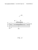
USPC Class:
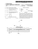
385129
Class name: Optical waveguides planar optical waveguide
Publication date: 2013-11-28
Patent application number: 20130315546
Abstract:
An optical PCB includes a substrate, conductive traces, a solder resist
layer, and a light waveguide. The substrate includes a surface. The
surface includes a flat area. The conductive traces are formed on the
surface of the substrate and only positioned outside of the flat area.
The solder resist layer is formed on the substrate and covers the
conductive traces. The light waveguide is positioned on the solder resist
layer. An orthogonal projection of the light waveguide on the surface of
the substrate coincides with the flat area.Claims:
1. An optical PCB, comprising: a substrate comprising a surface, the
surface comprising a flat area; a plurality of conductive traces formed
on the surface of the substrate and only positioned outside of the flat
area; a solder resist layer formed on the substrate and covering the
conductive traces; and a light waveguide positioned on the solder resist
layer, an orthogonal projection of the light waveguide on the surface of
the substrate coinciding with the flat area.
2. The optical PCB of claim 1, wherein a material of the solder resist layer is selected from the group consisting of ultraviolet curable printing ink and liquid photosensitive printing ink.
3. The optical PCB of claim 1, wherein the light waveguide is selected from the group consisting of planar light waveguide and strip light waveguide.
4. The optical PCB of claim 1, wherein the optical PCB comprises an adjusting sheet positioned between the substrate and the solder resist layer in the flat area.
5. The optical PCB of claim 4, wherein two opposite surfaces of the adjusting sheet are flat surfaces.
6. The optical PCB of claim 4, wherein the adjusting sheet has a same thickness as the conductive traces.
Description:
BACKGROUND
[0001] 1. Technical Field
[0002] The present disclosure relates to an optical printed circuit board (PCB).
[0003] 2. Description of Related Art
[0004] An optical PCB is a PCB that can transmit information using optical signals. Many optical PCBs include an insulated substrate, a printed circuit layer formed on a surface of the substrate, a solder resist layer applied to the printed circuit layer, and light waveguides positioned on the solder resist layer. The surface of the printed circuit layer will be uneven because of conductive traces. As such, the surface of the solder resist layer, on which the light waveguides are positioned, will not be flat, which makes it difficult to precisely position the light waveguides.
[0005] What is needed therefore is an optical PCB addressing the limitations described.
BRIEF DESCRIPTION OF THE DRAWINGS
[0006] The components of the drawings are not necessarily drawn to scale, the emphasis instead being placed upon clearly illustrating the principles of the embodiments of the present disclosure. Moreover, in the drawings, like reference numerals designate corresponding parts throughout several views.
[0007] FIG. 1 is a cross-sectional schematic view of an optical PCB, according to a first exemplary embodiment of the present disclosure.
[0008] FIG. 2 is a cross-sectional schematic view of an optical PCB, according to a second exemplary embodiment of the present disclosure.
DETAILED DESCRIPTION
[0009] FIG. 1 shows an optical PCB 100 according to a first exemplary embodiment. The optical PCB 100 includes a substrate 10, a number of conductive traces 20 formed on the substrate 10, a solder resist layer 30 formed on the substrate 10 and covering the conductive traces 20, and a light waveguide 40 positioned on a surface of the solder resist layer 30 opposite to the conductive traces 20.
[0010] The substrate 10 includes a first surface 101 and an opposite second surface 102. The first surface 101 includes a first area 103 substantially coinciding with an orthogonal projection of the light waveguide 40 on the first surface 101.
[0011] The conductive traces 20 form one or more printed circuits (not labeled) of the optical PCB 100. The conductive traces 20 are only formed outside of the first area 103 on the first surface 101. In other words, the first area 103 is kept clear of the conductive traces 20 to provide a flat expanse to more stably precisely mount the light waveguide 40. The conductive traces 20 are made from a highly conductive material, in this embodiment, the conductive traces 20 are made from copper.
[0012] The solder resist layer 30 provides a protective coating for the conductive traces 20 and prevents solder from bridging between conductors, thereby preventing short circuits. A material of the solder resist layer 30 can be selected from ultraviolet (UV) curable printing ink or liquid photosensitive printing ink.
[0013] The light waveguide 40 is configured for transmitting optical signals. The light waveguide 40 may be a type of planar light waveguide or a type of strip light waveguide.
[0014] Referring to FIG. 2, which shows an optical PCB 200 according to a second exemplary embodiment. Similar to the first embodiment, the optical PCB includes a substrate 50, a number of conductive traces 60 formed on the substrate 50, a solder resist layer 70 formed on the substrate 50 and covering the conductive traces 60, and a light waveguide 80 positioned on a surface of the solder resist layer 70. The substrate 50 includes a first surface 501 and an opposite second surface 502. The first surface 501 includes a first area 503 substantially coinciding with an orthogonal projection of the light waveguide 80 on the first surface 501. The first area 503 is kept clear of the conductive traces 60 to provide a flat expanse to more stably precisely mount the light waveguide 80. Different from the first embodiment, the optical PCB 200 further includes an adjusting sheet 90. The adjusting sheet 90 is positioned between the substrate 50 and the solder resist layer 70 covering the first area 503 of the first surface 501. The adjusting sheet 90 is configured for adjusting a height of the surface of the solder resist layer 70 above the first area 503 to adjust the height of the light waveguide 80 relative to the first surface 501, to align the light waveguide 80 with an optical/electrical element (not shown). Two opposite surfaces of the adjusting sheet 90 are flat surfaces. In this embodiment, the adjusting sheet 90 has the same thickness as the conductive traces 60 but may have a different thickness in other embodiments as required.
[0015] It is believed that the present embodiments and their advantages will be understood from the foregoing description, and it will be apparent that various changes may be made thereto without departing from the spirit and scope of the disclosure or sacrificing all of its material advantages, the examples hereinbefore described merely being preferred or exemplary embodiments of the disclosure.
User Contributions:
Comment about this patent or add new information about this topic:
| People who visited this patent also read: | |
| Patent application number | Title |
|---|---|
| 20150044481 | SURFACE PROTECTIVE SHEET, ELECTRONIC DEVICE, AND METHOD FOR MANUFACTURING ELECTRONIC DEVICE COMPONENT |
| 20150044480 | POLYURETHANE IMPREGNATED PAPER LAMINATE AND METHOD THEREFOR |
| 20150044479 | Ultraviolet-Curable Resin Composition |
| 20150044478 | METHOD FOR PRODUCING A COLOUR AND/OR EFFECT-PRODUCING MULTI-LAYERED COATING |
| 20150044477 | MEMBER FOR VEHICLE AND MANUFACTURING PROCESS FOR THE SAME |
Images included with this patent application:
 |  |
 |
| Similar patent applications: | |
| Date | Title |
|---|---|
| 2011-01-13 | Printed circuit board |
| 2013-12-05 | Flexible circuit board |
| 2009-04-30 | Optical termination unit |
| 2009-07-30 | Optical pulse compressor |
| 2010-03-25 | Optical circuit |
| New patent applications from these inventors: | |
| Date | Title |
|---|---|
| 2015-12-17 | Laser projection device |
| 2015-02-05 | Circuit board assembly with pads and connection lines having same resistance value as the pads and impedance matching method |
| 2014-12-25 | Mems-based rapidscan device and projector having same |
| 2014-12-18 | Mems-based rapidscan device and projector having same |
| 2014-11-27 | Miniature projection device |
| Top Inventors for class "Optical waveguides" | |
| Rank | Inventor's name |
|---|---|
| 1 | James Phillip Luther |
| 2 | Trevor D. Smith |
| 3 | Ming-Jun Li |
| 4 | Micah Colen Isenhour |
| 5 | Dennis Michael Knecht |