Patent application title: PHOTORESIST REMOVAL METHOD AND PATTERNING PROCESS UTILIZING THE SAME
Inventors:
Hung-Yi Wu (Keelung City, TW)
Hung-Yi Wu (Keelung City, TW)
Yuan-Chi Pai (Tainan City, TW)
Yuan-Chi Pai (Tainan City, TW)
Yu-Wei Cheng (Kaohsiung City, TW)
Chang-Mao Wang (Tainan City, TW)
Assignees:
UNITED MICROELECTRONICS CORP.
IPC8 Class: AH01L21306FI
USPC Class:
438708
Class name: Vapor phase etching (i.e., dry etching) utilizing electromagnetic or wave energy photo-induced etching
Publication date: 2013-08-15
Patent application number: 20130210237
Abstract:
A photoresist removal method is described. A substrate having thereon a
positive photoresist layer to be removed is provided. The positive
photoresist layer is UV-exposed without using a photomask. A development
liquid is used to remove the UV-exposed positive photoresist layer. The
substrate as provided may further have thereon a sacrificial masking
layer under the positive photoresist layer. The sacrificial masking layer
is removed after the UV-exposed positive photoresist layer is removed.Claims:
1. A photoresist removal method, comprising: providing a substrate having
thereon a positive photoresist layer to be removed; UV-exposing the
positive photoresist layer without using a photomask; and using a
development liquid to remove the UV-exposed positive photoresist layer.
2. The photoresist removal method of claim 1, wherein the positive photoresist layer on the substrate provided is a patterned positive photoresist layer.
3. The photoresist removal method of claim 2, wherein the substrate provided further has thereon a patterned sacrificial masking layer under the patterned positive photoresist layer, the method further comprising: removing the patterned sacrificial masking layer after the UV-exposed patterned positive photoresist layer is removed.
4. The photoresist removal method of claim 3, wherein the patterned sacrificial masking layer comprises a patterned bottom anti-reflective coating (BARC), or a patterned sacrificial light-absorbing material (SLAM) layer.
5. The photoresist removal method of claim 4, wherein the patterned BARC comprises a patterned light-absorbing oxide material (DUO).
6. The photoresist removal method of claim 4, wherein removing the patterned sacrificial masking layer comprises using a solvent.
7. The photoresist removal method of claim 2, wherein the patterned positive photoresist layer exposes a part of a MOS transistor.
8. The photoresist removal method of claim 7, wherein the exposed part of the MOS transistor includes a gate dielectric layer of the MOS transistor.
9. The photoresist removal method of claim 8, wherein the gate dielectric layer of the MOS transistor comprises a high-K layer.
10. A patterning process, comprising: providing a substrate having thereon a material layer to be patterned; forming a patterned positive photoresist layer over the material layer; removing the material layer not under the patterned positive photoresist layer; UV-exposing the patterned positive photoresist layer without using a photomask; and using a development liquid to remove the UV-exposed patterned positive photoresist layer.
11. The patterning process of claim 10, further comprising: forming a sacrificial masking layer over the material layer before the patterned positive photoresist layer is formed; patterning the sacrificial masking layer using the patterned positive photoresist layer as a mask after the patterned positive photoresist layer is formed but before the material layer not under the patterned positive photoresist layer is removed; and removing the patterned sacrificial masking layer after the UV-exposed patterned positive photoresist layer is removed.
12. The patterning process of claim 11, wherein the sacrificial masking layer comprises a bottom anti-reflective coating (BARC), or a sacrificial light-absorbing material (SLAM) layer.
13. The patterning process of claim 12, wherein the BARC comprises a light-absorbing oxide material (DUO).
14. The patterning process of claim 12, wherein removing the patterned sacrificial masking layer comprises using a solvent.
15. The patterning process of claim 10, wherein a part of a first MOS transistor is exposed after the material layer not under the patterned positive photoresist layer is removed.
16. The patterning process of claim 15, wherein the material layer comprising a gate material of a second MOS transistor, and the exposed part of the first MOS transistor comprises a gate dielectric layer of the first MOS transistor.
17. The patterning process of claim 16, wherein the gate material comprises a work-function metal, and the gate dielectric layer comprises a high-K layer.
18. The patterning process of claim 16, wherein one of the first and the second MOS transistors is a NMOS transistor and the other is a PMOS transistor.
Description:
BACKGROUND OF THE INVENTION
[0001] 1. Field of Invention
[0002] This invention relates to an integrated circuit (IC) process, and more particularly relates to a photoresist removal method, and a patterning process utilizing the photoresist removal method.
[0003] 2. Description of Related Art
[0004] In IC manufacturing, a patterned photoresist layer is traditionally removed using oxygen plasma after the patterns thereof are transferred to the target layer. However, oxygen plasma causes oxidation and bombardment damage to the underlying film stack.
[0005] In order to avoid oxidation and bombardment damage, a solvent such as OK73® or LA95® can be used to strip the patterned photoresist layer. However, such wet clean process has a lower photoresist cleaning effect because the solvent is difficult to remove the hybrid layer between the photoresist and the bottom anti-reflective coating (BARC). The solvent for removing the BARC is also difficult to remove the hybrid layer, so that the BARC under the hybrid layer either cannot be completely removed.
SUMMARY OF THE INVENTION
[0006] Accordingly, this invention provides a photoresist removal method without the problems of the oxygen plasma treatment and/or solvent stripping.
[0007] This invention also provides a patterning process that utilizes the photoresist removal method of this invention.
[0008] The photoresist removal method of this invention is described as follows. A substrate having thereon a positive photoresist layer to be removed is provided. The positive photoresist layer is UV-exposed without using a photomask. A development liquid is used to remove the UV-exposed positive photoresist layer.
[0009] The patterning process of this invention is described as follows. A substrate having thereon a material layer to be patterned is provided. A patterned positive photoresist layer is formed over the material layer. The material layer not under the patterned positive photoresist layer is removed. The above photoresist removal method of this invention is performed to remove the patterned positive photoresist layer.
[0010] In an embodiment, a sacrificial masking layer is formed over the material layer before the patterned positive photoresist layer is formed, and is patterned using the patterned positive photoresist layer as a mask after the patterned positive photoresist layer is formed but before the material layer not under the patterned positive photoresist layer is removed. The sacrificial masking layer is removed, possibly using a solvent, after the UV-exposed patterned positive photoresist layer is removed.
[0011] Since exposure and development are utilized instead of O2 plasma or a stripping solvent in the photoresist removal method of this invention, the under layer does not suffer from oxidation or damage, and the photoresist removal efficiency is not lower.
[0012] In order to make the aforementioned and other objects, features and advantages of the present invention comprehensible, a preferred embodiment accompanied with figures is described in detail below.
BRIEF DESCRIPTION OF THE DRAWINGS
[0013] FIGS. 1-6 illustrate, in a cross-sectional view, a patterning process according to an embodiment of this invention, wherein FIGS. 4-6 also illustrate a photoresist removal method according to the embodiment.
DESCRIPTION OF EMBODIMENTS
[0014] It is noted that the following embodiment is intended to further explain this invention but not to limit its scope. Specifically, although the photoresist removal method is applied to a patterning process in a high-K and metal-gate CMOS process in the following embodiment, it can be applied to any other patterning process as long as the under layers sustain UV-exposure and the development liquid.
[0015] FIGS. 1-6 illustrate, in a cross-sectional view, a patterning process according to an embodiment of this invention, wherein FIGS. 4-6 also illustrate a photoresist removal method according to the embodiment.
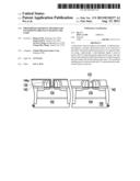
[0016] Referring to FIG. 1, a semiconductor substrate 100 to be formed with a CMOS device is provided, having thereon a NMOS area 102 and a PMOS area 104. A P-well 108 is formed in the substrate 100 in the NMOS area 102. An N-well 110 is formed in the substrate 100 in the PMOS area 104. A gate dielectric layer 120, which may be a single high-K layer or a film stack including a high-K layer, is formed on the substrate 100 in each of the NMOS area 102 and the PMOS area 104. When the gate dielectric layer 120 is a film stack including a high-K layer, other layers therein may include a dielectric liner under the high-K layer and a diffusion barrier layer on the high-K layer.
[0017] In addition, N-type source/drain (S/D) regions 122 of the NMOS are formed in the P-well 108, and P-type S/D regions 124 of the PMOS are formed in the N-well 110. A hole 130 for forming a metal gate of the NMOS is formed over the NMOS area 102, surrounded by a (double) spacer 136, a contact etching stop layer (CESL) 140a applying a tensile stress, and a dielectric layer 142. A hole 132 for forming a metal gate of the PMOS is formed over the PMOS area 104, surrounded by a (double) spacer 136, a CESL 140b applying a compressive stress, and the dielectric layer 142. Each of the holes 130 and 132 is formed by removing a dummy gate formed previously.
[0018] A work-function metal layer 144 suitable for the gate of N-type device is formed substantially conformally over the above structure, filling in the gate holes 130 and 132. Examples of the work-function metal material suitable for the gates of N-type devices include, but are not limited to, TiAl, ZrAl, WAl, TaAl and HfAl. However, one of ordinary skill in the art would easily realize that the material of the work function metal layer 144 is not limited to the abovementioned metals; it can be other material having a work function between about 3.9 eV and about 4.3 eV. Because the work-function metal layer 144 suitable for a NMOS gate is not suitable for a PMOS gate, the portion thereof on the PMOS area 104 has to be removed.
[0019] Referring to FIG. 2, a sacrificial masking layer 150 and a positive photoresist layer 152 are then formed over the substrate 100, wherein the sacrificial masking layer 150 fills in the holes 130 and 132 for forming metal gates. The sacrificial masking layer 150 is a layer having a superior gap-filling characteristic, such as a bottom anti-reflective coating (BARC) or a sacrificial light-absorbing material (SLAM) layer, but is not limited thereto. The BARC may include a light-absorbing oxide material (DUO), such as DUO248® (made by Honeywell Electronic Materials, a silicon-rich BARC material containing an organosiloxane-based polymer), but is not limited thereto. A photomask 154 having thereon an opaque pattern 156 masking the NMOS area 102 is used to perform a UV-exposure step 158, so that the portion of the positive photoresist layer 152 on the PMOS area 104 is UV-exposed. The UV-exposure step 158 may have a dose of 30-40 mJ/cm2.
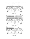
[0020] Referring to FIG. 3, the UV-exposed portion of the positive photoresist layer 152 on the PMOS area 104 is removed using a development liquid. The development liquid contains an alkaline compound, such as tetramethylammonium hydroxide (TMAH). The portions of the sacrificial masking layer 150 and the work-function metal layer 144 exposed thereby are removed using the patterned positive photoresist layer 152a as a mask, exposing the gate dielectric layer 120 in the hole 132 on the PMOS area 104. The remaining sacrificial masking layer 150a and the remaining work-function metal layer 144a are located on the NMOS area 102 only.
[0021] Referring to FIG. 4, another UV-exposure step 160 is performed to the entire substrate 100 without using a photomask, so that the patterned positive photoresist layer 152a is UV-exposed. The UV-exposure 160 may have a dose of 45-50 mJ/cm2.
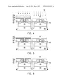
[0022] Referring to FIG. 5, the patterned positive photoresist layer 152a having been UV-exposed is then removed using a development liquid, which usually has the same composition of the development liquid used to pattern the positive photoresist layer 152 (FIG. 3) in the previous patterning procedure of the work-function metal layer 144.
[0023] Referring to FIG. 6, a solvent is used to remove the patterned sacrificial masking layer 150a. For example, when the sacrificial masking layer 150a includes DUO248®, the solvent can be CLK-888® that mainly includes 2,3,4,5-tetrahydrothiophene-1,1-dioxide (C4H8O2S, sulfolane), tertamethylammonium hydroxide [(CH3)4NOH, TMAH] and H2O.
[0024] After the above patterning process of this embodiment, it is possible to deposit over the substrate 100 another work-function metal layer suitable for the PMOS gate, deposit a low-resistance metal layer filling up the holes 130 and 132, and then remove the metal layers outside of the holes 130 and 132 to form metal gates of the NMOS and PMOS transistors (not shown).
[0025] Besides, though the work-function metal layer for the NMOS gate is patterned to expose the gate dielectric layer of the PMOS in the above embodiment, the photoresist removal method of this invention can also be applied to a case where the work-function metal layer for a PMOS gate is patterned to expose the gate dielectric layer of NMOS.
[0026] Since exposure and development are utilized instead of O2 plasma or a stripping solvent in the photoresist removal method of this invention, the under layer does not suffer from oxidation or damage, and the photoresist removal efficiency is not lowered.
[0027] This invention has been disclosed above in the preferred embodiments, but is not limited to those. It is known to persons skilled in the art that some modifications and innovations may be made without departing from the spirit and scope of this invention. Hence, the scope of this invention should be defined by the following claims.
User Contributions:
Comment about this patent or add new information about this topic:
| People who visited this patent also read: | |
| Patent application number | Title |
|---|---|
| 20130231269 | Multicomponent Viscoelastic Surfactant Fluid and Method of Using as a Fracturing Fluid |
| 20130231268 | Stabilized Acid Precursor and Acid-Enzyme Formulations for Drilling Mud Cake Removal |
| 20130231267 | ADENOVIRAL ASSEMBLY METHOD |
| 20130231266 | METHODS AND COMPOSITIONS REDUCING TARGET GENE EXPRESSION USING COCKTAILS OF siRNAS OR CONSTRUCTS EXPRESSING siRNAS |
| 20130231265 | TYROSINE KINASE BIOSENSORS AND METHODS OF USE |
Images included with this patent application:
 |  |
 |
| Similar patent applications: | |
| Date | Title |
|---|---|
| 2011-09-08 | Photoresist removing processor and methods |
| 2013-08-29 | Solar cell made in a single processing chamber |
| 2013-09-26 | Direct bonding process using a compressible porous layer |
| 2013-11-14 | Material sheet handling system and processing methods |
| 2013-09-05 | Photoresist structures having resistance to peeling |
| New patent applications in this class: | |
| Date | Title |
|---|---|
| 2016-01-07 | Process for treating a structure |
| 2015-12-24 | Apparatus for etching two-dimensional material and method of patterning two-dimensional material using the same |
| 2015-04-09 | Method for integrated circuit fabrication |
| 2015-02-19 | Lithography apparatus, and method of manufacturing article |
| 2014-10-09 | Phase shift mask, method of forming asymmetric pattern, method of manufacturing diffraction grating, and method of manufacturing semiconductor device |
| New patent applications from these inventors: | |
| Date | Title |
|---|---|
| 2016-04-14 | Semiconductor device and method for fabricating the same |
| 2016-02-04 | Method for fabricating semiconductor device |
| 2015-12-31 | Method of manufacturing semiconductor device |
| 2015-12-17 | Method of correcting overlay error |
| 2015-08-27 | Semiconductor structure and manufacturing method of the same |
| Top Inventors for class "Semiconductor device manufacturing: process" | |
| Rank | Inventor's name |
|---|---|
| 1 | Shunpei Yamazaki |
| 2 | Shunpei Yamazaki |
| 3 | Kangguo Cheng |
| 4 | Chen-Hua Yu |
| 5 | Devendra K. Sadana |