Patent application title: Method For Fabricating An Interlayer Conducting Structure Of An Embedded Circuitry
Inventors:
Chien-Wei Chang (Taoyuan, TW)
Ting-Hao Lin (Taipei, TW)
Yu-Te Lu (Taoyuan, TW)
IPC8 Class: AH05K300FI
USPC Class:
29829
Class name: Electrical device making conductor or circuit manufacturing on flat or curved insulated base, e.g., printed circuit, etc.
Publication date: 2011-04-14
Patent application number: 20110083323
Inventors list |
Agents list |
Assignees list |
List by place |
Classification tree browser |
Top 100 Inventors |
Top 100 Agents |
Top 100 Assignees |
Usenet FAQ Index |
Documents |
Other FAQs |
Patent application title: Method For Fabricating An Interlayer Conducting Structure Of An Embedded Circuitry
Inventors:
Ting-Hao Lin
Chien-Wei Chang
Yu-Te Lu
Agents:
Assignees:
Origin: ,
IPC8 Class: AH05K300FI
USPC Class:
Publication date: 04/14/2011
Patent application number: 20110083323
Abstract:
A method for fabricating an interlayer conducting structure of an
embedded circuitry is disclosed. In accordance with the method for
fabricating an interlayer conducting structure of an embedded circuitry
of the present invention, there is no laser conformal mask formed prior
to laminating the first and second lamination plates. Instead, after the
first and second lamination plates are laminated, a laser boring process
is directly conducted to form a via hole. In such a way, even when there
is an offset between the first and the second lamination plates in
alignment, the risk of short circuit between different layers of
lamination plates can be lowered without improving an interlayer offset
value.Claims:
1. A method for fabricating an interlayer conducting structure of an
embedded circuitry, comprising: forming a first circuitry and at least
one target point on a first lamination plate; forming a second circuitry
on a second lamination plate; laminating the second lamination plate on
the first lamination plate, wherein the second lamination plate overlaps
the first circuitry and the at least one target point; targeting the at
least one target point for positioning; executing a boring method to form
a via hole through the second lamination plate positioned on a stop pad
of the first circuitry; providing a photoresist layer on a part of the
second lamination layer and a part of the second circuitry; executing an
electroplating process to form a conductive layer in the via hole and on
the rest part of the second lamination plate which is uncovered by the
photoresist layer for electrically connecting the first circuitry with
the second circuitry; and removing the photoresist layer.
2. The method according to claim 1, wherein the boring process is a laser boring process employing a mask for determining a beam size of the laser and a diameter of the via hole.
3. The method according to claim 2, wherein the laser boring process bores the via hole with a UV-YAG laser, or a UV-excimer laser.
4. The method according to claim 1, wherein the via hole is a blind via hole or a buried via hole.
5. The method according to claim 1, wherein the photoresist layer is a dry film photoresist or a wet film photoresist
6. The method according to claim 1, wherein the conductive layer is a metal layer.
Description:
BACKGROUND OF THE INVENTION
[0001] 1. Field of the Invention
[0002] The present invention relates generally to a method for fabricating an interlayer conducting structure of an embedded circuitry. More particularly, according to the method of the present invention, there is no laser conformal mask formed prior to laminating the lamination plates. Instead, after the lamination plates are laminated, a laser boring process is conducted to form a via hole. In such a way, the risk of short circuit between different layers of lamination plates can be lowered without improving an interlayer offset value.
[0003] 2. The Prior Arts
[0004] For obtaining a larger area for wiring, most current printed circuit boards (PCB) are multilayer PCBs. Circuitries of different layers of such a multilayer PCB are typically connected by via holes, blind holes, or buried holes. However, since the multilayer PCB is fabricated by laminating a plurality of lamination plates one by one, there is often an offset when aligning different lamination plates for laminating.
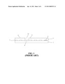
[0005] Referring to FIG. 1, it is a schematic diagram illustrating a conventional interlayer conducting structure. As shown in FIG. 1, a first circuitry 7 and a target point 5 are formed on a first lamination plate 1. A conformal mask pattern 9 is formed on a second circuitry 11 by executing a laser conformal mask processing thereon. The second lamination plate 3 is then laminated to the first lamination plate 1. Then, a laser boring process is executed to bore from the conformal mask 9 of the second lamination pate 3 through the second lamination plate 3 positioned on a stop pad of the first circuitry 7, thus forming a via hole 14 which ends at the stop pad of the first circuitry 7.
[0006] In this conventional technology of fabricating the interlayer conducting structure, the conformal mask is formed prior to laminating the first and second lamination plates. As such, any alignment offset between different lamination plates may lead to an offset between the conformal mask and the stop pad. Correspondingly, the via hole may be bored down through the second lamination plate 3, as shown in the A portion indicated in FIG. 1, which brings the risk of short circuit.
SUMMARY OF THE INVENTION
[0007] A primary objective of the present invention is to provide a method for fabricating an interlayer conducting structure of an embedded circuitry. In accordance with the present invention, a first circuitry lamination plate having a first circuitry and a target point formed thereon is laminated with a second lamination plate having a second circuitry formed thereon. Then, the target point is targeted and accorded to for executing a laser boring process to bore through the second lamination plate positioned on a stop pad of the first circuitry, such that a via hole is configured on the stop pad. Then, a photoresist layer is formed on a part of the second lamination plate and a part of the second circuitry, and a conductive layer is then formed on the via hole and the rest part of the second lamination plate which is uncovered by the photoresist layer. Finally, the photoresist layer is removed away.
[0008] In accordance with the method for fabricating an interlayer conducting structure of an embedded circuitry of the present invention, there is no laser conformal mask formed prior to laminating the first and second lamination plates. Instead, after the first and second lamination plates are laminated, a laser boring process is directly conducted to form a via hole. In such a way, even when there is an offset between the first and the second lamination plates in alignment, the risk of short circuit between different layers of lamination plates can be lowered without improving an interlayer offset value.
BRIEF DESCRIPTION OF THE DRAWINGS
[0009] The present invention will be apparent to those skilled in the art by reading the following detailed description of preferred embodiments thereof, with reference to the attached drawings, in which:
[0010] FIG. 1 is a schematic diagram illustrating a conventional interlayer conducting structure; and
[0011] FIGS. 2 through 6 illustrate steps of a method for fabricating an interlayer conducting structure of an embedded circuitry according to an embodiment of the present invention, wherein each of FIGS. 2 through 6 includes a schematic top view and a schematic side view, respectively, for illustration.
DETAILED DESCRIPTION OF THE PREFERRED EMBODIMENT
[0012] The accompanying drawings are included to provide a further understanding of the invention, and are incorporated in and constitute a part of this specification. The drawing illustrates embodiments of the invention and, together with the description, serves to explain the principles of the invention.
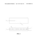
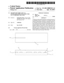
[0013] FIGS. 2 through 6 are schematic side views and top views illustrating steps of a method for fabricating an interlayer conducting structure of an embedded circuitry according to an embodiment of the present invention. Referring to FIG. 2, at first, a first lamination plate 1 is prepared, on which a first circuitry 7 and at least one target point 5 are formed. A second lamination plate 3 is prepared, on which a second circuitry 11 is formed. The second lamination plate 3 is then laminated on the first lamination plate 1. As shown in FIG. 2, the second lamination plate 3 overlaps the first circuitry 7 and the target point 5.
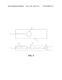
[0014] Then, referring to FIG. 3, the target point 5 is targeted for positioning and accorded to for executing a boring process to bore through the second lamination plate 3 positioned on a stop pad of the first circuitry 7, such that a via hole 13 is configured on the stop pad. Preferably, the boring process is a laser boring process, in which a mask is employed for determining a beam size of the laser and the diameter of the via hole 13. The laser boring process is executed in accordance with the position of the targeted target point 5 for alignment.
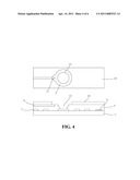
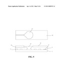
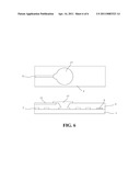
[0015] Then, referring to FIG. 4, a photoresist layer 15 is formed on a part of the second lamination plate 3 and a part of the second circuitry 11, and a conductive layer 17 is then formed in the via hole 13 and on the rest part of the second lamination plate 3 which is uncovered by the photoresist layer 15 by electroplating. Therefore, the first circuitry 7 is electrically connected with the second circuitry 11 as shown in FIG. 5. Finally, as shown in FIG. 6, the photoresist layer 15 is removed away.
[0016] It is worth to mention that the via hole 13 can be either a blind via hold or a buried via hole, the conductive layer 17 can be a metal layer, the photoresist layer 15 can be a dry film photoresist or a wet film photoresist, and the laser boring process may bore the via hole with a UV-YAG laser, or a UV-excimer laser.
[0017] In accordance with the method for fabricating an interlayer conducting structure of an embedded circuitry of the present invention, there is no laser conformal mask formed prior to laminating the first and second lamination plates. Instead, after the first and second lamination plates are laminated, a laser boring process is directly conducted to form a via hole. In such a way, even when there is an offset between the first and the second lamination plates in alignment, the risk of short circuit between different layers of lamination plates can be lowered without improving an interlayer offset value.
[0018] Although the present invention has been described with reference to the preferred embodiments thereof, it is apparent to those skilled in the art that a variety of modifications and changes may be made without departing from the scope of the present invention which is intended to be defined by the appended claims.
User Contributions:
comments("1"); ?> comment_form("1"); ?>Inventors list |
Agents list |
Assignees list |
List by place |
Classification tree browser |
Top 100 Inventors |
Top 100 Agents |
Top 100 Assignees |
Usenet FAQ Index |
Documents |
Other FAQs |
User Contributions:
Comment about this patent or add new information about this topic:
| People who visited this patent also read: | |
| Patent application number | Title |
|---|---|
| 20110097932 | CONNECTOR |
| 20110097931 | SHIELD CASE, AND CONNECTOR HAVING THE SAME |
| 20110097930 | RECEPTACLE FOR COAXIAL CONNECTOR |
| 20110097929 | Coaxial Plug-Connector Part with Ball |
| 20110097928 | Locking Ratcheting Torque Aid |
Images included with this patent application:
 |  |
 |  |
 |  |
 |
| New patent applications in this class: | |
| Date | Title |
|---|---|
| 2016-03-03 | Method of manufacturing printed wiring board |
| 2015-12-17 | Method for manufacturing multilayer substrate for having bga-type component thereon |
| 2015-11-12 | Electronic apparatus and method for assembling the same |
| 2015-05-14 | Led module sealing technology |
| 2015-03-05 | Preparation method of one glass solution touch screen |
| New patent applications from these inventors: | |
| Date | Title |
|---|---|
| 2017-05-18 | Modified magnetic coil structure |
| 2015-10-01 | Method of manufacturing a multilayer substrate structure for fine line |
| 2015-10-01 | Multilayer substrate structure for fine line |
| 2014-10-02 | Method of packaging a chip and a substrate |
| 2014-10-02 | Package structure of a chip and a substrate |
| Top Inventors for class "Metal working" | |
| Rank | Inventor's name |
|---|---|
| 1 | Levi A. Campbell |
| 2 | Robert E. Simons |
| 3 | Branko Sarh |
| 4 | Richard C. Chu |
| 5 | Shou-Shan Fan |