Patent application title: THERMAL PROTECT PCRAM STRUCTURE AND METHODS FOR MAKING
Inventors:
Shih-Hung Chen (Hsinchu, TW)
Shih-Hung Chen (Hsinchu, TW)
Assignees:
MACRONIX INTERNATIONAL CO., LTD.
IPC8 Class: AH01L4700FI
USPC Class:
257 2
Class name: Active solid-state devices (e.g., transistors, solid-state diodes) bulk effect device bulk effect switching in amorphous material
Publication date: 2011-01-20
Patent application number: 20110012079
d herein includes a conductive contact and a
memory element comprising programmable resistance memory material
overlying the conductive contact. An insulator element extends from the
conductive contact into the memory element, the insulator element having
proximal and distal ends and an inside surface defining an interior. The
proximal end is adjacent the conductive contact. A bottom electrode
contacts the conductive contact and extends upwardly within the interior
from the proximal end. The memory element is within the interior
extending downwardly from the distal end to contact a top surface of the
bottom electrode at a first contact surface. A top electrode can be
separated from the distal end of the insulator element by the memory
element and contact the memory element at a second contact surface having
a surface area greater than that of the first contact surface.Claims:
1. A memory device comprising:a conductive contact;a memory element
comprising programmable resistance memory material overlying the
conductive contact;an insulator element extending from the conductive
contact into the memory element, the insulator element having proximal
and distal ends and an inside surface defining an interior, the proximal
end adjacent the conductive contact; anda bottom electrode contacting the
conductive contact and extending upwardly within the interior from the
proximal end, the memory element within the interior extending downwardly
from the distal end to contact a top surface of the bottom electrode at a
first contact surface.
2. The memory device of claim 1, wherein the memory element has a bottom surface lying below the top surface of the bottom electrode.
3. The memory device of claim 1, wherein the memory element within the interior is self-aligned with the bottom electrode.
4. The memory device of claim 1, wherein the interior has a width less than a minimum feature size for a lithographic process used to form the memory device.
5. The memory device of claim 1, further comprising a top electrode separated from the distal end of the insulator element by the memory element and contacting the memory element at a second contact surface, the second contact surface having a surface area greater than that of the first contact surface.
6. The memory device of claim 1, wherein the memory element comprises material having a thermal conductivity less than that of material of the insulator element.
7. The memory device of claim 1, wherein the interior has substantially the same width at the proximal and distal ends.
8. A method for manufacturing a memory device, the method comprising:forming a conductive contact;forming an insulator element having proximal and distal ends and an inside surface defining an interior, the proximal end adjacent the conductive contact;forming a bottom electrode contacting the conductive contact and extending upwardly within the interior from the proximal end, the bottom electrode having a top surface; andforming a memory element comprising programmable resistance memory material on the insulator element, the memory element surrounding an outer surface of the insulator element and within the interior extending downwardly from the distal end to contact the top surface of the bottom electrode at a first contact surface.
9. The method of claim 8, wherein the memory element has a bottom surface lying below the top surface of the bottom electrode.
10. The method of claim 8, wherein forming the bottom electrode comprises:filling the interior defined by the inside surface of the insulator element with bottom electrode material; andremoving the bottom electrode material from an upper portion of the interior to form the bottom electrode.
11. The method of claim 8, wherein the interior has a width less than a minimum lithographic feature size for a lithographic process used to form the memory device.
12. The method of claim 8, further comprising forming a top electrode separated from the distal end of the insulator element by the memory element and contacting the memory element at a second contact surface, the second contact surface having a surface area greater than that of the first contact surface.
13. The method of claim 8, wherein the memory element comprises material having a thermal conductivity less than that of material of the insulator element.
14. The method of claim 8, wherein the interior has substantially the same width at the proximal and distal ends.
15. The method of claim 8, wherein forming the insulator element comprises:forming a first material layer and forming a second material layer on the first material layer;forming a via in the first and second material layers to expose the conductive contact, the via having a sidewall; andforming the insulator element on the sidewall of the via.
16. The method of claim 15, wherein forming the insulator element on the sidewall of the via comprises:depositing a layer of insulator material within the via including on the sidewall of the via; andanisotropically etching the insulator material.
17. The method of claim 15, wherein forming the bottom electrode and forming the memory element comprise:filling the interior defined by the inner surface of the insulator element with bottom electrode material;removing the bottom electrode material from the upper portion of the interior to form the bottom electrode from remaining bottom electrode material;removing the second material layer to expose the outside surface of the insulator element; anddepositing memory material within the upper portion of the interior and on the exposed outside surface of the insulator element.
18. The method of claim 8, wherein forming the insulator element and forming the bottom electrode comprise:forming the insulator element on a sidewall of a via;filling the interior defined by the inner surface of the insulator element with bottom electrode material; andremoving the bottom electrode material from the upper portion of the interior to form the bottom electrode from remaining bottom electrode material.
19. A memory device comprising:a pipe shaped insulator element having an inside surface defining an interior, and having an outer surface;a first electrode within a lower portion of the interior;a memory element comprising programmable resistance memory material within an upper portion of the interior contacting the top surface of the first electrode at a first contact surface, the memory element having an active region within the upper portion; anda second electrode contacting the memory element at a second contact surface.
20. The memory device of claim 19, wherein the memory element surrounds the outer surface of the pipe shaped insulator element.Description:
BACKGROUND OF THE INVENTION
[0001]1. Field of the Invention
[0002]The present invention relates to memory devices based on phase change memory materials, including chalcogenide based materials and other programmable resistance materials, and methods for manufacturing such devices.
[0003]2. Description of Related Art
[0004]Phase change based memory materials, like chalcogenide based materials and similar materials, can be caused to change phase between an amorphous and a crystalline state by application of electrical current at levels suitable for implementation in integrated circuits. The generally amorphous state is characterized by higher electrical resistivity than the generally crystalline state, which can be readily sensed to indicate data. These properties have generated interest in using programmable resistance material to form nonvolatile memory circuits, which can be read and written with random access.
[0005]The change from the amorphous to the crystalline, referred to as set herein, is generally a lower current operation in which current heats the phase change material above a transition temperature to cause a transition of an active region from the amorphous to the crystalline phase. The change from the crystalline to the amorphous, referred to as reset herein, is generally a higher current operation, which includes a short high current density pulse to melt or breakdown the crystalline structure, after which phase change material cools quickly, quenching the phase change process and allowing at least a portion of the active region of the phase change material to stabilize in the amorphous phase. Techniques are applied to make the active region small, so that the amount of current needed to induce the phase change is reduced.
[0006]The magnitude of the current needed can be reduced by reducing the size of the phase change material element and/or the size of electrodes in contact with the phase change material element, so that higher current densities are achieved in the active region with small absolute current values.
[0007]One approach to controlling the size of the active region is to devise very small electrodes for delivering current to a body of phase change material. This small electrode structure concentrates current in a small area like the head of a mushroom, at the location of the contact. See, U.S. Pat. No. 6,429,064, issued Aug. 6, 2002 to Wicker, "Reduced Contact Areas of Sidewall Conductor"; U.S. Pat. No. 6,462,353, issued Oct. 8, 2002, to Gilgen, "Method for Fabricating a Small Area of Contact Between Electrodes"; U.S. Pat. No. 6,501,111, issued Dec. 31, 2002, to Lowrey, "Three-Dimensional (3D) Programmable Device"; U.S. Pat. No. 6,563,156, issued Jul. 1, 2003, to Harshfield, "Memory Elements and Methods for Making Same".
[0008]Another approach to controlling the size of the active region includes spacing the electrodes in such a way that current flowing therebetween is concentrated by the thickness of a thin layer of phase change material. See, U.S. Patent Application Publication No. US 2007/0048945, entitled "Memory Device and Method of Making Same", by Czubatyj, et al. See also the following applications and patents commonly owned by the assignee of the present application: U.S. patent application Ser. No. 11/864,273, filed 28 Sep. 2007, entitled "Memory Cell Having A Side Electrode Contact", by Lung; U.S. Pat. No. 7,463,512, issued 9 Dec. 2008, entitled "Memory Element with Reduced-Current Phase Change Element", by Lung; U.S. application Ser. No. 12/023,978, filed 7 Aug. 2008, entitled "Memory Cell Device with Coplanar Electrode Surface and Method", by Lung.
[0009]A specific issue arising from conventional phase change memory cell structures is the heat sink effect of electrodes in contact with the phase change material. Because the phase change occurs as a result of heating, the thermal conductivity of the electrodes will act to draw heat away from the active region, resulting in a need for a higher current to induce the desired phase change.
[0010]Higher current levels can result in electrical and mechanical reliability problems for the memory cell. These problems include the formation of voids at the phase change material/electrode interface due to mechanical stress caused by thermal expansion and material density changes during operation.
[0011]Additionally, higher current levels can result in problems such as localized heating sufficient to induce diffusion/reaction of electrode and phase change material, and/or cause compositional changes in the phase change material within the active region, resulting in resistive switching performance degradation and possible failure of the memory cell.
[0012]Thus, various techniques are used in an attempt to thermally isolate the active region so that the resistive heating needed to induce the phase change is confined to the active region.
[0013]One approach to improving thermal isolation includes using gaps or voids adjacent the phase change material. See U.S. Pat. No. 6,815,704, issued 9 Nov. 2004, entitled "Phase Change Memory Device Employing Thermally Insulating Voids", by Chen.
[0014]It has also been proposed to use thermally insulating materials to improve the confinement of heat to the active region. See, for example, U.S. patent application Ser. No. 11/940164, filed 14 Nov. 2007, entitled "Phase Change Memory Cell Including Thermal Protect Bottom Electrode and Manufacturing Methods", by Chen.
[0015]Another approach to improving thermal isolation includes forming the phase change material and electrodes in a way that tends to space the active region from the electrodes. See the following applications commonly owned by the assignee of the present application: U.S. patent application Ser. No. 11/348,848, filed 7 Sep. 2006, entitled "I-Shaped Phase Change Memory Cell", by Chen et al.; U.S. patent application Ser. No. 11/952646, filed 7 Dec. 2007, entitled "Phase Change Memory Cell Having Interface Structures with Essentially Equal thermal Impedances and Manufacturing Methods", by Lung; U.S. application Ser. No. 12/026342, filed 5 Feb. 2005, entitled "Heating Center PCRAM Structure and Methods for Making", by Chen.
[0016]Accordingly, an opportunity arises to devise phase change memory cell structures requiring a small amount of current to induce phase change in the active region. Furthermore, it is desirable to provide methods for manufacturing such devices.
SUMMARY OF THE INVENTION
[0017]Phase change based memory cells having small operational currents are described herein. The memory cells described herein reduce the amount of heat drawn away from the active region of the memory element, effectively increasing the amount of heat generated within the active region per unit value of current and thus reducing the amount of current required to induce phase change.
[0018]A memory cell as described herein includes a conductive contact and a memory element comprising programmable resistance memory material overlying the conductive contact. An insulator element extends from the conductive contact into the memory element, the insulator element having proximal and distal ends and an inside surface defining an interior. The proximal end is adjacent the conductive contact. A bottom electrode contacts the conductive contact and extends upwardly within the interior from the proximal end. Memory material of the memory element is within the interior extending downwardly from the distal end to contact a top surface of the bottom electrode at a first contact surface. A top electrode can be separated from the distal end of the insulator element by memory material of the memory element and contacts the memory element at a second contact surface. The second contact surface can have a surface area greater than that of the first contact surface.
[0019]The active region is the region of the memory element within the interior in which the memory material is induced to change between at least two solid phases. As can be appreciated, the active region can be made extremely small, thus reducing the magnitude of the current needed to induce a phase change. The width of the interior is less than the width of the memory element and the top electrode, the width of the interior preferably less than a minimum feature size for a process, typically a lithographic process, used to form the memory cell. The difference in widths concentrates current in the portion of the memory element within the upper portion of the interior, thereby reducing the magnitude of current needed to induce a phase change in the active region.
[0020]In addition, the bottom electrode can act as a heater, because of its high resistivity in certain embodiments, inducing a greater temperature change in the active region for a given current flow than would otherwise occur, thus improving the efficiency of the phase change in the active region.
[0021]Furthermore, the small width of the bottom electrode provides a high thermal resistance path through the bottom electrode, thus restricting the amount of heat flow away from the active region of the memory element through the bottom electrode.
[0022]Since the insulator element extends into the memory element and in embodiments has a bottom surface lying below the top surface of the bottom electrode, the active region is inside the volume of memory material of the memory element. The remaining portions of the memory element can therefore provide thermal isolation to the active region, which reduces the amount of current necessary to induce a phase change. In addition, having the active region within the upper portion of the interior, and thus spaced away from the outside surfaces of memory element, prevents etch damage issues to the active region.
[0023]The insulator element can also provide some thermal isolation to the active region. Additionally, the insulator element can be formed on a sidewall using thin film deposition techniques, and thus the thickness of the element can be very small. The small thickness increases the thermal resistance of the sidewall insulator element, which restricts heat flow away from the active region by the sidewall insulator element and thereby helps to concentrates the heat flow to within the material of the memory element.
[0024]Other aspects and advantages of the present invention can be seen on review of the drawings, the detailed description, and the claims which follow.
BRIEF DESCRIPTION OF THE DRAWINGS
[0025]FIG. 1 illustrates a cross-sectional view of a prior art "mushroom-type" memory cell.
[0026]FIG. 2 illustrates a cross-sectional view of a prior art "pillar-type" memory cell.
[0027]FIGS. 3A and 3B are cross-sectional and top views respectively of an embodiment of a memory cell described herein.
[0028]FIGS. 4 to 9 illustrate steps in a fabrication sequence suitable for manufacturing the memory cell of FIGS. 3A-3B.
[0029]FIG. 10 is a simplified block diagram of an integrated circuit in which the memory cells described herein can be implemented.
[0030]FIG. 11 is a schematic diagram of a portion of an embodiment of the memory array of the integrated circuit of FIG. 10.
DETAILED DESCRIPTION
[0031]A detailed description of embodiments of the present invention is provided with reference to the FIGS. 1-11.
[0032]FIG. 1 illustrates a cross-sectional view of a prior art "mushroom-type" memory cell 100 having a bottom electrode 120 extending through a dielectric layer 110, a phase change memory element 130 comprising a layer of phase change material on the bottom electrode 120, and a top electrode 140 on the phase change memory element 130. A dielectric layer 160 surrounds the phase change memory element 130. As can be seen in FIG. 1, the bottom electrode 120 has a width 125 less than the width 145 of the top electrode 140 and phase change material 130.
[0033]In operation, voltages on the top and bottom electrodes 140, 120 induce a current to flow from the top electrode 140 to the bottom electrode 120, or vice-versa, via the phase change memory element 130.
[0034]The active region 150 is the region of the phase change memory element 130 in which the phase change material is induced to change between at least two solid phases. Due to the differences in the widths 125 and 145, the current flow path 180 from the bottom electrode 120 to the top electrode 140 is concentrated in the region of the phase change memory element 130 adjacent the bottom electrode 120, resulting in the active region 150 having a "mushroom" shape as shown in FIG. 1.
[0035]It is desirable to minimize the width 125 of the bottom electrode 120 so that higher current densities are achieved with small absolute current values through the memory element 130. However, attempts to reduce the width 125 of the bottom electrode 120 can result in issues in the electrical and mechanical reliability of the interface 128 between the bottom electrode 120 and the memory element 130 due to the small contact surface therebetween.
[0036]In operation, due to the differences in widths 125 and 145 the current is concentrated at the contact surface 128 between the bottom electrode 120 and the phase change memory element 130. In addition, as indicated by the arrows of path 180, the current flow from the contact surface 128 spreads laterally and vertically within the phase change memory element 130. As a result, the current density within the phase change memory element 130 deceases with distance away from the contact surface 128 in both the lateral and vertical directions. This decrease in current density caused by the current spreading within the memory element 130 results in a need for higher current to induce the desired phase change in the active region 150.
[0037]The current density and thus the heat generated at the center 152 of the active region 150 is much larger than at the edges 154 of the active region 150. As a result, when the edges 154 of the active region 150 are heated to a temperature sufficient to induce the desired phase change, the center 152 can experience localized heating sufficient to cause electrical and mechanical reliability problems for the memory cell 100.
[0038]These problems can include the formation voids at the interface 128 between the phase change memory element 130 and the bottom electrode 120 due to mechanical stress caused by thermal expansion and material density changes during operation. In addition, the center 152 may experience localized heating sufficient to induce diffusion/reaction of material of the bottom electrode 120 and the phase change material 130, and/or may cause compositional changes in the phase change material 130 at the center 154. These problems can result in resistive switching performance degradation and possible failure of the memory cell 100.
[0039]Additionally, because the phase change in the active region 150 occurs as a result of heating, the thermal conductivity of the bottom electrode 120 and dielectric 110 will act to draw heat away from the active region 150 and result in a significant amount of heat loss. The high heat loss results in a need for a higher current to induce the desired change in the active region 150.
[0040]FIG. 2 illustrates a cross-sectional view of a prior art "pillar-type" memory cell 200. The memory cell 200 includes a bottom electrode 220 in a dielectric layer 210, a pillar of phase change material 230 on the bottom electrode 220, and a top electrode 240 on the pillar of phase change material 230. A dielectric layer 260 surrounds the pillar of phase change material 230. As can be seen in the Figure, the top and bottom electrodes 240, 220 have the same width 275 as that of the pillar of phase change material 230. Thus, the active region 250 can be spaced away from the top and bottom electrodes 240, 220, resulting in a reduced heat sink effect by the top and bottom electrodes 240, 220. However, there is heat loss through the sidewalls 232 of the phase change material 230 to the dielectric layer 260 due to the proximity of the active region 250 to the dielectric layer 260.
[0041]It is desirable to minimize the width 275 of the pillar of phase change material 230 so that higher current densities are achieved with small absolute current values through the phase change material 230. The pillar of memory material 230 and the top electrode 240 can be formed by depositing a phase change material layer and a layer of top electrode material, and then etching. However problems have arisen in manufacturing devices having small widths 275 and aggressive aspect ratios due to issues with undercut etching and/or overetching. This can result in etch damage to the to the sidewalls 232 of the pillar of memory material 230, as well as alignment tolerance issues between the pillar of memory material 230 and the bottom electrode 220.
[0042]FIG. 3A is a cross-sectional view of an embodiment of a memory cell 300 as described herein having a small operating current and addressing the various issues described above.
[0043]The memory cell 300 includes a conductive contact 305 and a programmable resistance memory element 330 overlying the conductive contact 305. The conductive contact 305 couples the memory cell 300 to underlying access circuitry (not shown) such as a transistor or diode. The conductive contact 305 comprises a refractory metal such as tungsten in the illustrated embodiment. Other metals that could be used include Ti, Mo, Al, Ta, Cu, Pt, Ir, La, Ni, and Ru. Other contact structures and materials can be used as well. For example, the conductive contact 305 may be a silicide or may comprise a doped semiconductor material which is a drain or source region of an access transistor or a terminal of a diode.
[0044]The memory element 330 comprises programmable resistance memory material and may comprise, for example, one or more materials from the group of Zn, To, Tl, Ge, Sb, Te, Se, In, Ti, Ga, Bi, Sn, Cu, Pd, Pb, Ag, S, Si, O, P, As, N and Au.
[0045]The memory cell 300 also includes a pipe shaped insulator element 350 extending from the conductive contact 305 into the memory element 330. The insulator element 350 has a proximal end 356 adjacent the conductive contact 305 and a distal end 351. The insulator element 350 also has an inside surface 354 defining an interior 360. The insulator element 350 comprises dielectric material, and in the illustrated embodiment comprises Al2O3. Alternatively, the insulator element 350 may comprise other dielectric materials, for example SiO2 or SiN.
[0046]A bottom electrode 320 contacts the conductive contact 305 and extends upwardly within a bottom portion 362 of the interior 360 from the proximal end 356. The inside surface 354 of the insulator element 350 extends above the top surface 324 of the bottom electrode 320 to define an upper portion 364 of the interior 360. In the illustrated embodiment the upper and lower portions 364, 362 have substantially the same width 366. As used herein, the term "substantially" is intended to accommodate manufacturing tolerances during the formation of the insulator element 350.
[0047]The bottom electrode 320 has an outer surface 322 surrounded by the inside surface 354 of the insulator element 350. The bottom electrode 320 may comprise, for example, for example, TiN or TaN. TiN may be preferred in embodiments in which the memory element 330 comprises GST (discussed below) because is makes a good contact with GST, it is a common material used in semiconductor manufacturing, and it provides a good diffusion barrier at the higher temperatures at which GST transitions, typically in the 600-700° C. range. Alternatively, the bottom electrode 320 may be W, WN, TiAlN or TaAlN, or comprise, for further examples, one or more elements selected from the group consisting of doped-Si, Si, Ge, C, Ge, Cr, Ti, W, Mo, Al, Ta, Cu, Pt, Ir, La, Ni, N, O, and Ru and combinations thereof.
[0048]As shown in the top view of FIG. 3B, in the illustrated embodiment the bottom electrode 320 and the insulator element 350 each have a circular cross-section. However, in embodiments the bottom electrode 320 and the insulator element 350 may respectively have a cross-section that is circular, elliptical, square, rectangular or somewhat irregularly shaped, depending on the manufacturing technique applied to form the bottom electrode 320 the insulator element 350.
[0049]Referring back to the cross-section of FIG. 3A, the memory element 330 includes a portion within the upper portion 364 of the interior 360 extending downwardly from the distal end 351 to contact the top surface 324 of the bottom electrode 320 at a first contact surface 333.
[0050]The memory element 330 also extends below the top surface of the insulator element 350 to contact the outer surface 352 of the insulator element 350, and has a bottom surface 331 lying below the top surface 324 of the bottom electrode 320. As a result, the memory element 330 surrounds portions of the insulator element 350 and the bottom electrode 320.
[0051]The memory element 330 is on dielectric 310. The dielectric 310 may comprise, for example, SiO2. Alternatively, the dielectric 310 may comprise other materials.
[0052]The memory cell 300 also includes a top electrode 340 separated from the distal end 351 of the insulator element 350 by memory material of the memory element 330. The top electrode 340 contacts the memory element 330 at a second contact surface 342. The second contact surface 342 has a surface area greater than that of the first contact surface 333.
[0053]The top electrode 340 may comprise, for example, any of the materials discussed above with reference to the bottom electrode 320. In some embodiments the top electrode 340 may comprise more than one layer. For example, the top electrode 340 may comprise a first material contacting the memory element 330 and chosen for compatibility with the material of memory element 330, and a second material on the first and chosen for other advantages such as a lower electrical resistivity. In some embodiments the top electrode 340 may comprise a portion of a bit line. The top electrode 340 and memory element 330 are surrounded by dielectric 370 comprising, for example, SiO2. Alternatively, the dielectric 370 may comprise other materials.
[0054]In operation, voltages on the top electrode 340 and the bottom electrode 320 induce a current to flow along path 380 from the top electrode 340 to the bottom electrode 320, or vice versa, through the memory element 330 via contact surfaces 333, 342.
[0055]The active region is the portion of the memory element 330 within the upper portion 364 of the interior 360 in which the memory material is induced to change between at least two solid phases. As can be appreciated, the active region can be made extremely small in the illustrated structure, thus reducing the magnitude of the current needed to induce a phase change. The width 366 of the interior 360 is less than the width 332 of the memory element 330 and top electrode 340, the width 366 preferably less than a minimum feature size for a process, typically a lithographic process, used to form the memory cell 300. The difference in widths 332 and 366 confines current in the portion of the memory element 330 within the upper portion 364 of the interior 360, thereby reducing the magnitude of current needed to induce a phase change in the active region.
[0056]In addition, the bottom electrode 320 can act as a heater, because of its high resistivity in certain embodiments, inducing a greater temperature change in the active region for a given current flow than would otherwise occur, thus improving the efficiency of the phase change in the active region.
[0057]Furthermore, the small width 366 of the bottom electrode 320 provides a high thermal resistance path through the bottom electrode 320, thus restricting the amount of heat flow away from the active region of the memory element 330 through the bottom electrode 320.
[0058]Since the memory element 330 surrounds the outer surface 352 of the insulator element 350 and extends below the top surface 324 of the bottom electrode 320, the active region is inside the volume of memory material of the memory element 330. The remaining portions of the memory element 330 can therefore provide thermal isolation to the active region, which reduces the amount of current necessary to induce a phase change. In embodiments the memory material of the memory element 330 can have a thermal conductivity (k) in the highest thermal conductivity state less than that of the dielectric materials 310, 350, and 370. Thus, by having the active region inside the volume of memory material, in embodiments the memory element 330 can provide greater thermal isolation to the active region than would be provided by dielectric materials, thus reducing the amount of current necessary to induce a phase change.
[0059]In addition, having the active region within the upper portion 364 of the interior 360, and thus spaced away from the outside surfaces of memory element 330, prevents etch damage issues to the active region.
[0060]The insulator element 350 can also provide some thermal isolation to the active region. Additionally, in embodiments the insulator element 350 can be formed on a sidewall using thin film deposition techniques, and thus the thickness 352 of the insulator element 350 can be very small. The small thickness 352 increases the thermal resistance of the insulator element 350, which restricts heat flow away from the active region by the insulator element 350 and thereby helps to concentrate the heat flow to within the material of the memory element 330.
[0061]FIGS. 4 to 9 illustrate steps in a fabrication sequence suitable for manufacturing the memory cell 300 of FIGS. 3A-3B.
[0062]FIG. 4 illustrates a first step of forming dielectric 310 on conductive contact 305, forming a sacrificial material layer 400 on dielectric 310, and forming a via 410 in the material layer 400 and dielectric 310, the via 410 having a sidewall surface 414. The material layer 400 comprises material that can be selectively processed (e.g. selectively etched) relative to the material of dielectric 310 and the subsequently formed sidewall insulator element 350. The material layer 400 may comprise, for example SiO2, while dielectric and the subsequently formed sidewall insulator element 350 may each comprise SiN.
[0063]The via 410 having a sublithographic width 412 can be formed, for example, by forming an isolation layer on the layer 400 and forming a sacrificial layer on the isolation layer. Next, a mask having an opening close to or equal to the minimum feature size of the process used to create the mask is formed on the sacrificial layer, the opening overlying the location of the via 41 0. The isolation layer and the sacrificial layer are then selectively etched using the mask, thereby forming a via in the isolation and sacrificial layers and exposing a top surface of the layer 400. After removal of the mask, a selective undercutting etch is performed on the via such that the isolation layer is etched while leaving the sacrificial layer and the layer 400 intact. A fill material is then formed in the via, which due to the selective undercutting etch process results in a self-aligned void in the fill material being formed within the via. Next, an anisotropic etching process is performed on the fill material to open the void, and etching continues until the layer 400 is exposed in the region below the via, thereby forming a sidewall spacer comprising fill material within the via. The sidewall spacer has an opening dimension substantially determined by the dimension of the void, and thus can be less than the minimum feature size of a lithographic process. Next, the layer 400 and dielectric 310 are etched using the sidewall spacer as an etch mask, thereby forming via 410 having a width 412 less than the minimum lithographic feature size. The isolation layer and the sacrificial layer can be removed by a planarization process such as Chemical Mechanical Polishing (CMP).
[0064]Next, a layer 500 of insulator material is formed on the structure illustrated in FIG. 4, including within the via 410, resulting in the structure illustrated the cross-sectional view of FIG. 5. As can be seen in the FIG. 4, the layer 500 is conformal with the via 410 and is on the sidewall 414. The layer 500 can be formed, for example, by chemical vapor deposition (CVD) or atomic layer deposition (ALD).
[0065]Next, the layer 500 of insulator material of the structure of FIG. 5 is anisotropically etched to form the insulator element 350 on the sidewall 414 of the via 410, resulting in the structure illustrated in the cross-sectional view of FIG. 6. The insulator element 350 has an inner surface 354 defining an interior 360.
[0066]Next, bottom electrode 320 is formed within the interior 360 of the insulator element 350 of the structure illustrated in FIG. 6, resulting in the structure illustrated in the cross-sectional view of FIG. 7. The bottom electrode 320 can be formed, for example, by depositing a layer of bottom electrode material on the structure illustrated in FIG. 6, followed by a planarization process such as Chemical Mechanical Polishing (CMP) to expose the top surface of the material layer 400.
[0067]Next, a portion of the bottom electrode 320 is etched from the structure illustrated in FIG. 7, resulting in the bottom electrode 320 having a top surface 324 below the top surface 351 of the insulator element 350 as illustrated in the cross-sectional view of FIG. 8. The etching of a portion of the bottom electrode 320 results in the upper portion 364 of the interior 360 being self-aligned with the remaining portion of the bottom electrode 320 within the lower portion 362. As a result, the memory material subsequently formed within the interior is self-aligned with the bottom electrode 320.
[0068]Next, material layer 400 is selectively etched from the structure illustrated in FIG. 8 to expose the outer surface 352 of the insulator element 350, and the top surface of the bottom electrode 320 is cleaned, resulting in the structure illustrated in the cross-sectional view of FIG. 9. In the illustrated embodiment the material layer 400 is SiO2 and the insulator element 350 and layer 310 are SiN, and the selective etching may be performed, for example, using HF.
[0069]Next, phase change material is deposited on the structure illustrated in FIG. 9, top electrode material is deposited on the phase change material, and the phase change material and top electrode material are patterned to form the memory element 330 and top electrode 340 respectively, resulting in the memory cell 300 of FIGS. 3A-3B.
[0070]FIG. 10 is a simplified block diagram of an integrated circuit 1000 including a memory array 1005 having memory cells as described herein having small operational currents, the memory cells including phase change memory elements programmable to a plurality of resistance states including a lower resistance state and a higher resistance state. A word line decoder 1010 having read, reset, reset verify, set verify, and set modes is coupled to and in electrical communication with a plurality of word lines 1015 arranged along rows in the memory array 1005. A bit line (column) decoder 1020 is in electrical communication with a plurality of bit lines 1025 arranged along columns in the array 1005 for reading and programming the memory cells (not shown) in array 1005.
[0071]Addresses are supplied on bus 1060 to word line decoder and drivers 1010 and bit line decoder 1020. Sense circuitry (Sense amplifiers) and data-in structures in block 1030, including voltage and/or current sources for the read and program modes are coupled to bit line decoder 1020 via data bus 1035. Data is supplied via a data-in line 1040 from input/output ports on integrated circuit 1000, or from other data sources internal or external to integrated circuit 1000, to data-in structures in block 1030. Other circuitry 1065 may be included on integrated circuit 1000, such as a general purpose processor or special purpose application circuitry, or a combination of modules providing system-on-a-chip functionality supported by array 1005. Data is supplied via a data-out line 1045 from the sense amplifiers in block 1030 to input/output ports on integrated circuit 1000, or to other data destinations internal or external to integrated circuit 1000.
[0072]The integrated circuit 1000 includes a controller 1050 for read, reset, reset verify, set verify, and set modes of the memory cells of the array 1005. The controller 1050, implemented in this example using a bias arrangement state machine, controls the application of bias circuitry voltage & current sources 1055 for the application of bias arrangements including read, set and reset to the word lines 1015, bit lines 1025, and in some embodiments source lines. Controller 1050 may be implemented using special-purpose logic circuitry as known in the art. In alternative embodiments, controller 1050 comprises a general-purpose processor, which may be implemented on the same integrated circuit to execute a computer program to control the operations of the device. In yet other embodiments, a combination of special-purpose logic circuitry and a general-purpose processor may be utilized for implementation of controller 1050.
[0073]As shown in FIG. 11, each of the memory cells of array 1005 includes an access transistor (or other access device such as a diode) and a phase change memory element. In FIG. 11 four memory cells 1130, 1132, 1134, 1136 having respective memory elements 1140, 1142, 1144, 1146 are illustrated, representing a small section of an array that can include millions of memory cells. The memory elements are programmable to a plurality of resistance states including a lower and a higher resistance state.
[0074]Sources of each of the access transistors of memory cells 1130, 1132, 1134, 1136 are connected in common to source line 1154 that terminates in source line termination circuit 1155, such as a ground terminal. In another embodiment the source lines of the access devices are not electrically connected, but independently controllable. The source line termination circuit 1155 may include bias circuitry such as voltage sources and current sources, and decoding circuits for applying bias arrangements, other than ground, to the source line 1154 in some embodiments.
[0075]A plurality of word lines including word lines 1156, 1158 extend in parallel along a first direction. Word lines 1156, 1158 are in electrical communication with word line decoder 1010. The gates of access transistors of memory cells 1130 and 1134 are connected to word line 1156, and the gates of access transistors of memory cells 1132 and 1136 are connected in common to word line 1158.
[0076]A plurality of bit lines including bit lines 1160, 1162 extend in parallel in a second direction and are in electrical communication with bit line decoder 1120. In the illustrated embodiment each of the memory elements are arranged between the drain of the corresponding access device and the corresponding bit line. Alternatively, the memory elements may be on the source side of the corresponding access device.
[0077]It will be understood that the memory array 1105 is not limited to the array configuration illustrated in FIG. 11, and additional array configurations can also be used. Additionally, instead of MOS transistors, bipolar transistors or diodes may be used as access devices in some embodiments.
[0078]In operation each of the memory cells in the array 1105 store data depending upon the resistance of the corresponding memory element. The data value may be determined, for example, by comparison of current on a bit line for a selected memory cell to that of a suitable reference current by sense amplifiers of sense circuitry 1 130. The reference current can be established to that a predetermined range of currents correspond to a logical "0", and a differing range of currents correspond to a logical "1". In a memory cell having three or more states, reference currents can be established so that differing ranges of bit line currents correspond to each of the three or more states.
[0079]Reading, or writing to a memory cell of array 1105 can be achieved by applying a suitable voltage to one of word lines 1156, 1158 and coupling one of bit lines 1160, 1162 to a voltage so that current flows through the selected memory cell. For example, a current path 1180 through a selected memory cell (in this example memory cell 1132 and corresponding memory element 1148) is established by applying voltages to the bit line 1160, word line 1158, and source line 1154 sufficient to turn on the access transistor of memory cell 1132 and induce current in path 1180 to flow from the bit line 1160 to the source line 1154, or vice-versa. The level and duration of the voltages applied is dependent upon the operation performed.
[0080]In a reset (or erase) operation of memory cell 1132, word line decoder 1010 facilitates providing word line 1158 with a suitable voltage to turn on the access transistor of the memory cell 1132. Bit line decoder 1020 facilitates supplying one or more voltage pulses to bit line 1160 of suitable amplitude and duration to induce a current to flow though memory element 1148, thereby raising the temperature of at least the active region above the transition temperature of the phase change material of the memory element 1148 and also above the melting temperature to place at least the active region in a liquid state. The current is then terminated, for example by terminating the voltage pulse on the bit line 1160 and the voltage on the word line 1158, resulting in a relatively quick quenching time as the active region rapidly cools to stabilize to an amorphous phase.
[0081]In a read (or sense) operation of memory cell 1132, word line decoder 1010 facilitates providing word line 1158 with a suitable voltage to turn on the access transistor of the memory cell 1132. Bit line decoder 1120 facilitates supplying a voltage to bit line 1160 of suitable amplitude and duration to induce current to flow that does not result in the memory element 1 148 undergoing a change in resistive state. The current on the bit line 1160 and through the memory element 1148 is dependent upon the resistance of, and therefore the data state associated with, the memory element 1148 of the memory cell 1132. Thus, the data state of the memory cell 1132 may be determined, for example by comparison of the current on bit line 1160 with a suitable reference current by sense amplifiers of sense circuitry 1030.
[0082]In a set (or program) operation of memory cell 1132, word line decoder 1010 facilitates providing word line 1158 with a suitable voltage to turn on the access transistor of the memory cell 1132. Bit line decoder 1020 facilitates supplying a voltage to bit line 1160 of suitable amplitude and duration to induce current to flow through the memory element 1148, thereby raising the temperature of a least a portion of the active region above the transition temperature of the phase change material to cause a transition of at least a portion of the active region from the amorphous phase to the crystalline phase, this transition lowering the resistance of the memory element 1148 and setting the memory cell 1132 to the desired state.
[0083]Embodiments of memory material of the memory elements described herein include phase change based memory materials, including chalcogenide based materials and other materials. Chalcogens include any of the four elements oxygen (O), sulfur (S), selenium (Se), and tellurium (Te), forming part of group VIA of the periodic table. Chalcogenides comprise compounds of a chalcogen with a more electropositive element or radical. Chalcogenide alloys comprise combinations of chalcogenides with other materials such as transition metals. A chalcogenide alloy usually contains one or more elements from group IVA of the periodic table of elements, such as germanium (Ge) and tin (Sn). Often, chalcogenide alloys include combinations including one or more of antimony (Sb), gallium (Ga), indium (In), and silver (Ag). Many phase change based memory materials have been described in technical literature, including alloys of: Ga/Sb, In/Sb, In/Se, Sb/Te, Ge/Te, Ge/Sb/Te, In/Sb/Te, Ga/Se/Te, Sn/Sb/Te, In/Sb/Ge, Ag/In/Sb/Te, Ge/Sn/Sb/Te, Ge/Sb/Se/Te and Te/Ge/Sb/S. In the family of Ge/Sb/Te alloys, a wide range of alloy compositions may be workable. The compositions can be characterized as TeaGebSb.sub.100-(a-b). One researcher has described the most useful alloys as having an average concentration of Te in the deposited materials well below 70%, typically below about 60% and ranged in general from as low as about 23% up to about 58% Te and most preferably about 48% to 58% Te. Concentrations of Ge were above about 5% and ranged from a low of about 8% to about 30% average in the material, remaining generally below 50%. Most preferably, concentrations of Ge ranged from about 8% to about 40%. The remainder of the principal constituent elements in this composition was Sb. These percentages are atomic percentages that total 100% of the atoms of the constituent elements. (Ovshinsky U.S. Pat. No. 5,687,112 patent, cols. 10-11.) Particular alloys evaluated by another researcher include Ge2Sb2Te5, GeSb2Te4 and GeSb4Te7 (Noboru Yamada, "Potential of Ge--Sb--Te Phase-Change Optical Disks for High-Data-Rate Recording", SPIE v. 3109, pp. 28-37 (1997).) More generally, a transition metal such as chromium (Cr), iron (Fe), nickel (Ni), niobium (Nb), palladium (Pd), platinum (Pt) and mixtures or alloys thereof may be combined with Ge/Sb/Te to form a phase change alloy that has programmable resistive properties. Specific examples of memory materials that may be useful are given in Ovshinsky '112 at columns 11-13, which examples are hereby incorporated by reference.
[0084]Chalcogenides and other phase change materials are doped with impurities in some embodiments to modify conductivity, transition temperature, melting temperature, and other properties of memory elements using the doped chalcogenides. Representative impurities used for doping chalcogenides include nitrogen, silicon, oxygen, silicon dioxide, silicon nitride, copper, silver, gold, aluminum, aluminum oxide, tantalum, tantalum oxide, tantalum nitride, titanium and titanium oxide. See, e.g., U.S. Pat. No. 6,800,504, and U.S. Patent Application Publication No. U.S. 2005/0029502.
[0085]Phase change alloys are capable of being switched between a first structural state in which the material is in a generally amorphous solid phase, and a second structural state in which the material is in a generally crystalline solid phase in its local order in the active channel region of the cell. These alloys are at least bistable. The term amorphous is used to refer to a relatively less ordered structure, more disordered than a single crystal, which has the detectable characteristics such as higher electrical resistivity than the crystalline phase. The term crystalline is used to refer to a relatively more ordered structure, more ordered than in an amorphous structure, which has detectable characteristics such as lower electrical resistivity than the amorphous phase. Typically, phase change materials may be electrically switched between different detectable states of local order across the spectrum between completely amorphous and completely crystalline states. Other material characteristics affected by the change between amorphous and crystalline phases include atomic order, free electron density and activation energy. The material may be switched either into different solid phases or into mixtures of two or more solid phases, providing a gray scale between completely amorphous and completely crystalline states. The electrical properties in the material may vary accordingly.
[0086]Phase change alloys can be changed from one phase state to another by application of electrical pulses. It has been observed that a shorter, higher amplitude pulse tends to change the phase change material to a generally amorphous state. A longer, lower amplitude pulse tends to change the phase change material to a generally crystalline state. The energy in a shorter, higher amplitude pulse is high enough to allow for bonds of the crystalline structure to be broken and short enough to prevent the atoms from realigning into a crystalline state. Appropriate profiles for pulses can be determined, without undue experimentation, specifically adapted to a particular phase change alloy. In following sections of the disclosure, the phase change material is referred to as GST, and it will be understood that other types of phase change materials can be used. A material useful for implementation of a PCRAM described herein is Ge2Sb2Te5.
[0087]Other programmable resistive memory materials may be used in other embodiments of the invention, including other materials that use different crystal phase changes to determine resistance, or other memory materials that use an electrical pulse to change the resistance state. Examples include materials for use in resistance random access memory (RRAM) such as metal-oxides including tungsten-oxide (WOx), NiO, Nb2O5, CuO2, Ta2O5, Al2O3, CoO, Fe2O3, HfO2, TiO2, SrTiO3, SrZrO3, (BaSr)TiO3, Additional examples include materials for use in magnetoresistance random access memory (MRAM) such as spin-torque-transfer (STT) MRAM, for example at least one of CoFeB, Fe, Co, Ni, Gd, Dy, CoFe, NiFe, MnAs, MnBi, MnSb, CrO2, MnOFe2O3, FeOFe2O5, NiOFe2O3, MgOFe2, EuO, and Y3Fe5O12. See, for example, US Publication No 2007/0176251 entitled "Magnetic Memory Device and Method of Fabricating the Same", which is incorporated by reference herein. Additional examples include solid electrolyte materials used for programmable-metallization-cell (PMC) memory, or nano-ionic memory, such as silver-doped germanium sulfide electrolytes and copper-doped germanium sulfide electrolytes. See, for example, N. E. Gilbert et al., "A macro model of programmable metallization cell devices," Solid-State Electronics 49 (2005) 1813-1819, which is incorporated by reference herein.
[0088]An exemplary method for forming chalcogenide material uses PVD-sputtering or magnetron-sputtering method with source gas(es) of Ar, N2, and/or He, etc. at the pressure of 1 mTorr˜100 mTorr. The deposition is usually done at room temperature. A collimator with an aspect ratio of 1˜5 can be used to improve the fill-in performance. To improve the fill-in performance, a DC bias of several tens of volts to several hundreds of volts is also used. On the other hand, the combination of DC bias and the collimater can be used simultaneously.
[0089]An exemplary method for forming chalcogenide material uses chemical vapor deposition CVD such as that disclosed in US Publication No 2006/0172067 entitled "Chemical Vapor Deposition of Chalcogenide Materials", which is incorporated by reference herein.
[0090]A post-deposition annealing treatment in a vacuum or in an N2 ambient is optionally performed to improve the crystallize state of chalcogenide material. The annealing temperature typically ranges from 100° C. to 400° C. with an anneal time of less than 30 minutes.
[0091]While the present invention is disclosed by reference to the preferred embodiments and examples detailed above, it is to be understood that these examples are intended in an illustrative rather than in a limiting sense. It is contemplated that modifications and combinations will readily occur to those skilled in the art, which modifications and combinations will be within the spirit of the invention and the scope of the following claims.
Claims:
1. A memory device comprising:a conductive contact;a memory element
comprising programmable resistance memory material overlying the
conductive contact;an insulator element extending from the conductive
contact into the memory element, the insulator element having proximal
and distal ends and an inside surface defining an interior, the proximal
end adjacent the conductive contact; anda bottom electrode contacting the
conductive contact and extending upwardly within the interior from the
proximal end, the memory element within the interior extending downwardly
from the distal end to contact a top surface of the bottom electrode at a
first contact surface.
2. The memory device of claim 1, wherein the memory element has a bottom surface lying below the top surface of the bottom electrode.
3. The memory device of claim 1, wherein the memory element within the interior is self-aligned with the bottom electrode.
4. The memory device of claim 1, wherein the interior has a width less than a minimum feature size for a lithographic process used to form the memory device.
5. The memory device of claim 1, further comprising a top electrode separated from the distal end of the insulator element by the memory element and contacting the memory element at a second contact surface, the second contact surface having a surface area greater than that of the first contact surface.
6. The memory device of claim 1, wherein the memory element comprises material having a thermal conductivity less than that of material of the insulator element.
7. The memory device of claim 1, wherein the interior has substantially the same width at the proximal and distal ends.
8. A method for manufacturing a memory device, the method comprising:forming a conductive contact;forming an insulator element having proximal and distal ends and an inside surface defining an interior, the proximal end adjacent the conductive contact;forming a bottom electrode contacting the conductive contact and extending upwardly within the interior from the proximal end, the bottom electrode having a top surface; andforming a memory element comprising programmable resistance memory material on the insulator element, the memory element surrounding an outer surface of the insulator element and within the interior extending downwardly from the distal end to contact the top surface of the bottom electrode at a first contact surface.
9. The method of claim 8, wherein the memory element has a bottom surface lying below the top surface of the bottom electrode.
10. The method of claim 8, wherein forming the bottom electrode comprises:filling the interior defined by the inside surface of the insulator element with bottom electrode material; andremoving the bottom electrode material from an upper portion of the interior to form the bottom electrode.
11. The method of claim 8, wherein the interior has a width less than a minimum lithographic feature size for a lithographic process used to form the memory device.
12. The method of claim 8, further comprising forming a top electrode separated from the distal end of the insulator element by the memory element and contacting the memory element at a second contact surface, the second contact surface having a surface area greater than that of the first contact surface.
13. The method of claim 8, wherein the memory element comprises material having a thermal conductivity less than that of material of the insulator element.
14. The method of claim 8, wherein the interior has substantially the same width at the proximal and distal ends.
15. The method of claim 8, wherein forming the insulator element comprises:forming a first material layer and forming a second material layer on the first material layer;forming a via in the first and second material layers to expose the conductive contact, the via having a sidewall; andforming the insulator element on the sidewall of the via.
16. The method of claim 15, wherein forming the insulator element on the sidewall of the via comprises:depositing a layer of insulator material within the via including on the sidewall of the via; andanisotropically etching the insulator material.
17. The method of claim 15, wherein forming the bottom electrode and forming the memory element comprise:filling the interior defined by the inner surface of the insulator element with bottom electrode material;removing the bottom electrode material from the upper portion of the interior to form the bottom electrode from remaining bottom electrode material;removing the second material layer to expose the outside surface of the insulator element; anddepositing memory material within the upper portion of the interior and on the exposed outside surface of the insulator element.
18. The method of claim 8, wherein forming the insulator element and forming the bottom electrode comprise:forming the insulator element on a sidewall of a via;filling the interior defined by the inner surface of the insulator element with bottom electrode material; andremoving the bottom electrode material from the upper portion of the interior to form the bottom electrode from remaining bottom electrode material.
19. A memory device comprising:a pipe shaped insulator element having an inside surface defining an interior, and having an outer surface;a first electrode within a lower portion of the interior;a memory element comprising programmable resistance memory material within an upper portion of the interior contacting the top surface of the first electrode at a first contact surface, the memory element having an active region within the upper portion; anda second electrode contacting the memory element at a second contact surface.
20. The memory device of claim 19, wherein the memory element surrounds the outer surface of the pipe shaped insulator element.
Description:
BACKGROUND OF THE INVENTION
[0001]1. Field of the Invention
[0002]The present invention relates to memory devices based on phase change memory materials, including chalcogenide based materials and other programmable resistance materials, and methods for manufacturing such devices.
[0003]2. Description of Related Art
[0004]Phase change based memory materials, like chalcogenide based materials and similar materials, can be caused to change phase between an amorphous and a crystalline state by application of electrical current at levels suitable for implementation in integrated circuits. The generally amorphous state is characterized by higher electrical resistivity than the generally crystalline state, which can be readily sensed to indicate data. These properties have generated interest in using programmable resistance material to form nonvolatile memory circuits, which can be read and written with random access.
[0005]The change from the amorphous to the crystalline, referred to as set herein, is generally a lower current operation in which current heats the phase change material above a transition temperature to cause a transition of an active region from the amorphous to the crystalline phase. The change from the crystalline to the amorphous, referred to as reset herein, is generally a higher current operation, which includes a short high current density pulse to melt or breakdown the crystalline structure, after which phase change material cools quickly, quenching the phase change process and allowing at least a portion of the active region of the phase change material to stabilize in the amorphous phase. Techniques are applied to make the active region small, so that the amount of current needed to induce the phase change is reduced.
[0006]The magnitude of the current needed can be reduced by reducing the size of the phase change material element and/or the size of electrodes in contact with the phase change material element, so that higher current densities are achieved in the active region with small absolute current values.
[0007]One approach to controlling the size of the active region is to devise very small electrodes for delivering current to a body of phase change material. This small electrode structure concentrates current in a small area like the head of a mushroom, at the location of the contact. See, U.S. Pat. No. 6,429,064, issued Aug. 6, 2002 to Wicker, "Reduced Contact Areas of Sidewall Conductor"; U.S. Pat. No. 6,462,353, issued Oct. 8, 2002, to Gilgen, "Method for Fabricating a Small Area of Contact Between Electrodes"; U.S. Pat. No. 6,501,111, issued Dec. 31, 2002, to Lowrey, "Three-Dimensional (3D) Programmable Device"; U.S. Pat. No. 6,563,156, issued Jul. 1, 2003, to Harshfield, "Memory Elements and Methods for Making Same".
[0008]Another approach to controlling the size of the active region includes spacing the electrodes in such a way that current flowing therebetween is concentrated by the thickness of a thin layer of phase change material. See, U.S. Patent Application Publication No. US 2007/0048945, entitled "Memory Device and Method of Making Same", by Czubatyj, et al. See also the following applications and patents commonly owned by the assignee of the present application: U.S. patent application Ser. No. 11/864,273, filed 28 Sep. 2007, entitled "Memory Cell Having A Side Electrode Contact", by Lung; U.S. Pat. No. 7,463,512, issued 9 Dec. 2008, entitled "Memory Element with Reduced-Current Phase Change Element", by Lung; U.S. application Ser. No. 12/023,978, filed 7 Aug. 2008, entitled "Memory Cell Device with Coplanar Electrode Surface and Method", by Lung.
[0009]A specific issue arising from conventional phase change memory cell structures is the heat sink effect of electrodes in contact with the phase change material. Because the phase change occurs as a result of heating, the thermal conductivity of the electrodes will act to draw heat away from the active region, resulting in a need for a higher current to induce the desired phase change.
[0010]Higher current levels can result in electrical and mechanical reliability problems for the memory cell. These problems include the formation of voids at the phase change material/electrode interface due to mechanical stress caused by thermal expansion and material density changes during operation.
[0011]Additionally, higher current levels can result in problems such as localized heating sufficient to induce diffusion/reaction of electrode and phase change material, and/or cause compositional changes in the phase change material within the active region, resulting in resistive switching performance degradation and possible failure of the memory cell.
[0012]Thus, various techniques are used in an attempt to thermally isolate the active region so that the resistive heating needed to induce the phase change is confined to the active region.
[0013]One approach to improving thermal isolation includes using gaps or voids adjacent the phase change material. See U.S. Pat. No. 6,815,704, issued 9 Nov. 2004, entitled "Phase Change Memory Device Employing Thermally Insulating Voids", by Chen.
[0014]It has also been proposed to use thermally insulating materials to improve the confinement of heat to the active region. See, for example, U.S. patent application Ser. No. 11/940164, filed 14 Nov. 2007, entitled "Phase Change Memory Cell Including Thermal Protect Bottom Electrode and Manufacturing Methods", by Chen.
[0015]Another approach to improving thermal isolation includes forming the phase change material and electrodes in a way that tends to space the active region from the electrodes. See the following applications commonly owned by the assignee of the present application: U.S. patent application Ser. No. 11/348,848, filed 7 Sep. 2006, entitled "I-Shaped Phase Change Memory Cell", by Chen et al.; U.S. patent application Ser. No. 11/952646, filed 7 Dec. 2007, entitled "Phase Change Memory Cell Having Interface Structures with Essentially Equal thermal Impedances and Manufacturing Methods", by Lung; U.S. application Ser. No. 12/026342, filed 5 Feb. 2005, entitled "Heating Center PCRAM Structure and Methods for Making", by Chen.
[0016]Accordingly, an opportunity arises to devise phase change memory cell structures requiring a small amount of current to induce phase change in the active region. Furthermore, it is desirable to provide methods for manufacturing such devices.
SUMMARY OF THE INVENTION
[0017]Phase change based memory cells having small operational currents are described herein. The memory cells described herein reduce the amount of heat drawn away from the active region of the memory element, effectively increasing the amount of heat generated within the active region per unit value of current and thus reducing the amount of current required to induce phase change.
[0018]A memory cell as described herein includes a conductive contact and a memory element comprising programmable resistance memory material overlying the conductive contact. An insulator element extends from the conductive contact into the memory element, the insulator element having proximal and distal ends and an inside surface defining an interior. The proximal end is adjacent the conductive contact. A bottom electrode contacts the conductive contact and extends upwardly within the interior from the proximal end. Memory material of the memory element is within the interior extending downwardly from the distal end to contact a top surface of the bottom electrode at a first contact surface. A top electrode can be separated from the distal end of the insulator element by memory material of the memory element and contacts the memory element at a second contact surface. The second contact surface can have a surface area greater than that of the first contact surface.
[0019]The active region is the region of the memory element within the interior in which the memory material is induced to change between at least two solid phases. As can be appreciated, the active region can be made extremely small, thus reducing the magnitude of the current needed to induce a phase change. The width of the interior is less than the width of the memory element and the top electrode, the width of the interior preferably less than a minimum feature size for a process, typically a lithographic process, used to form the memory cell. The difference in widths concentrates current in the portion of the memory element within the upper portion of the interior, thereby reducing the magnitude of current needed to induce a phase change in the active region.
[0020]In addition, the bottom electrode can act as a heater, because of its high resistivity in certain embodiments, inducing a greater temperature change in the active region for a given current flow than would otherwise occur, thus improving the efficiency of the phase change in the active region.
[0021]Furthermore, the small width of the bottom electrode provides a high thermal resistance path through the bottom electrode, thus restricting the amount of heat flow away from the active region of the memory element through the bottom electrode.
[0022]Since the insulator element extends into the memory element and in embodiments has a bottom surface lying below the top surface of the bottom electrode, the active region is inside the volume of memory material of the memory element. The remaining portions of the memory element can therefore provide thermal isolation to the active region, which reduces the amount of current necessary to induce a phase change. In addition, having the active region within the upper portion of the interior, and thus spaced away from the outside surfaces of memory element, prevents etch damage issues to the active region.
[0023]The insulator element can also provide some thermal isolation to the active region. Additionally, the insulator element can be formed on a sidewall using thin film deposition techniques, and thus the thickness of the element can be very small. The small thickness increases the thermal resistance of the sidewall insulator element, which restricts heat flow away from the active region by the sidewall insulator element and thereby helps to concentrates the heat flow to within the material of the memory element.
[0024]Other aspects and advantages of the present invention can be seen on review of the drawings, the detailed description, and the claims which follow.
BRIEF DESCRIPTION OF THE DRAWINGS
[0025]FIG. 1 illustrates a cross-sectional view of a prior art "mushroom-type" memory cell.
[0026]FIG. 2 illustrates a cross-sectional view of a prior art "pillar-type" memory cell.
[0027]FIGS. 3A and 3B are cross-sectional and top views respectively of an embodiment of a memory cell described herein.
[0028]FIGS. 4 to 9 illustrate steps in a fabrication sequence suitable for manufacturing the memory cell of FIGS. 3A-3B.
[0029]FIG. 10 is a simplified block diagram of an integrated circuit in which the memory cells described herein can be implemented.
[0030]FIG. 11 is a schematic diagram of a portion of an embodiment of the memory array of the integrated circuit of FIG. 10.
DETAILED DESCRIPTION
[0031]A detailed description of embodiments of the present invention is provided with reference to the FIGS. 1-11.
[0032]FIG. 1 illustrates a cross-sectional view of a prior art "mushroom-type" memory cell 100 having a bottom electrode 120 extending through a dielectric layer 110, a phase change memory element 130 comprising a layer of phase change material on the bottom electrode 120, and a top electrode 140 on the phase change memory element 130. A dielectric layer 160 surrounds the phase change memory element 130. As can be seen in FIG. 1, the bottom electrode 120 has a width 125 less than the width 145 of the top electrode 140 and phase change material 130.
[0033]In operation, voltages on the top and bottom electrodes 140, 120 induce a current to flow from the top electrode 140 to the bottom electrode 120, or vice-versa, via the phase change memory element 130.
[0034]The active region 150 is the region of the phase change memory element 130 in which the phase change material is induced to change between at least two solid phases. Due to the differences in the widths 125 and 145, the current flow path 180 from the bottom electrode 120 to the top electrode 140 is concentrated in the region of the phase change memory element 130 adjacent the bottom electrode 120, resulting in the active region 150 having a "mushroom" shape as shown in FIG. 1.
[0035]It is desirable to minimize the width 125 of the bottom electrode 120 so that higher current densities are achieved with small absolute current values through the memory element 130. However, attempts to reduce the width 125 of the bottom electrode 120 can result in issues in the electrical and mechanical reliability of the interface 128 between the bottom electrode 120 and the memory element 130 due to the small contact surface therebetween.
[0036]In operation, due to the differences in widths 125 and 145 the current is concentrated at the contact surface 128 between the bottom electrode 120 and the phase change memory element 130. In addition, as indicated by the arrows of path 180, the current flow from the contact surface 128 spreads laterally and vertically within the phase change memory element 130. As a result, the current density within the phase change memory element 130 deceases with distance away from the contact surface 128 in both the lateral and vertical directions. This decrease in current density caused by the current spreading within the memory element 130 results in a need for higher current to induce the desired phase change in the active region 150.
[0037]The current density and thus the heat generated at the center 152 of the active region 150 is much larger than at the edges 154 of the active region 150. As a result, when the edges 154 of the active region 150 are heated to a temperature sufficient to induce the desired phase change, the center 152 can experience localized heating sufficient to cause electrical and mechanical reliability problems for the memory cell 100.
[0038]These problems can include the formation voids at the interface 128 between the phase change memory element 130 and the bottom electrode 120 due to mechanical stress caused by thermal expansion and material density changes during operation. In addition, the center 152 may experience localized heating sufficient to induce diffusion/reaction of material of the bottom electrode 120 and the phase change material 130, and/or may cause compositional changes in the phase change material 130 at the center 154. These problems can result in resistive switching performance degradation and possible failure of the memory cell 100.
[0039]Additionally, because the phase change in the active region 150 occurs as a result of heating, the thermal conductivity of the bottom electrode 120 and dielectric 110 will act to draw heat away from the active region 150 and result in a significant amount of heat loss. The high heat loss results in a need for a higher current to induce the desired change in the active region 150.
[0040]FIG. 2 illustrates a cross-sectional view of a prior art "pillar-type" memory cell 200. The memory cell 200 includes a bottom electrode 220 in a dielectric layer 210, a pillar of phase change material 230 on the bottom electrode 220, and a top electrode 240 on the pillar of phase change material 230. A dielectric layer 260 surrounds the pillar of phase change material 230. As can be seen in the Figure, the top and bottom electrodes 240, 220 have the same width 275 as that of the pillar of phase change material 230. Thus, the active region 250 can be spaced away from the top and bottom electrodes 240, 220, resulting in a reduced heat sink effect by the top and bottom electrodes 240, 220. However, there is heat loss through the sidewalls 232 of the phase change material 230 to the dielectric layer 260 due to the proximity of the active region 250 to the dielectric layer 260.
[0041]It is desirable to minimize the width 275 of the pillar of phase change material 230 so that higher current densities are achieved with small absolute current values through the phase change material 230. The pillar of memory material 230 and the top electrode 240 can be formed by depositing a phase change material layer and a layer of top electrode material, and then etching. However problems have arisen in manufacturing devices having small widths 275 and aggressive aspect ratios due to issues with undercut etching and/or overetching. This can result in etch damage to the to the sidewalls 232 of the pillar of memory material 230, as well as alignment tolerance issues between the pillar of memory material 230 and the bottom electrode 220.
[0042]FIG. 3A is a cross-sectional view of an embodiment of a memory cell 300 as described herein having a small operating current and addressing the various issues described above.
[0043]The memory cell 300 includes a conductive contact 305 and a programmable resistance memory element 330 overlying the conductive contact 305. The conductive contact 305 couples the memory cell 300 to underlying access circuitry (not shown) such as a transistor or diode. The conductive contact 305 comprises a refractory metal such as tungsten in the illustrated embodiment. Other metals that could be used include Ti, Mo, Al, Ta, Cu, Pt, Ir, La, Ni, and Ru. Other contact structures and materials can be used as well. For example, the conductive contact 305 may be a silicide or may comprise a doped semiconductor material which is a drain or source region of an access transistor or a terminal of a diode.
[0044]The memory element 330 comprises programmable resistance memory material and may comprise, for example, one or more materials from the group of Zn, To, Tl, Ge, Sb, Te, Se, In, Ti, Ga, Bi, Sn, Cu, Pd, Pb, Ag, S, Si, O, P, As, N and Au.
[0045]The memory cell 300 also includes a pipe shaped insulator element 350 extending from the conductive contact 305 into the memory element 330. The insulator element 350 has a proximal end 356 adjacent the conductive contact 305 and a distal end 351. The insulator element 350 also has an inside surface 354 defining an interior 360. The insulator element 350 comprises dielectric material, and in the illustrated embodiment comprises Al2O3. Alternatively, the insulator element 350 may comprise other dielectric materials, for example SiO2 or SiN.
[0046]A bottom electrode 320 contacts the conductive contact 305 and extends upwardly within a bottom portion 362 of the interior 360 from the proximal end 356. The inside surface 354 of the insulator element 350 extends above the top surface 324 of the bottom electrode 320 to define an upper portion 364 of the interior 360. In the illustrated embodiment the upper and lower portions 364, 362 have substantially the same width 366. As used herein, the term "substantially" is intended to accommodate manufacturing tolerances during the formation of the insulator element 350.
[0047]The bottom electrode 320 has an outer surface 322 surrounded by the inside surface 354 of the insulator element 350. The bottom electrode 320 may comprise, for example, for example, TiN or TaN. TiN may be preferred in embodiments in which the memory element 330 comprises GST (discussed below) because is makes a good contact with GST, it is a common material used in semiconductor manufacturing, and it provides a good diffusion barrier at the higher temperatures at which GST transitions, typically in the 600-700° C. range. Alternatively, the bottom electrode 320 may be W, WN, TiAlN or TaAlN, or comprise, for further examples, one or more elements selected from the group consisting of doped-Si, Si, Ge, C, Ge, Cr, Ti, W, Mo, Al, Ta, Cu, Pt, Ir, La, Ni, N, O, and Ru and combinations thereof.
[0048]As shown in the top view of FIG. 3B, in the illustrated embodiment the bottom electrode 320 and the insulator element 350 each have a circular cross-section. However, in embodiments the bottom electrode 320 and the insulator element 350 may respectively have a cross-section that is circular, elliptical, square, rectangular or somewhat irregularly shaped, depending on the manufacturing technique applied to form the bottom electrode 320 the insulator element 350.
[0049]Referring back to the cross-section of FIG. 3A, the memory element 330 includes a portion within the upper portion 364 of the interior 360 extending downwardly from the distal end 351 to contact the top surface 324 of the bottom electrode 320 at a first contact surface 333.
[0050]The memory element 330 also extends below the top surface of the insulator element 350 to contact the outer surface 352 of the insulator element 350, and has a bottom surface 331 lying below the top surface 324 of the bottom electrode 320. As a result, the memory element 330 surrounds portions of the insulator element 350 and the bottom electrode 320.
[0051]The memory element 330 is on dielectric 310. The dielectric 310 may comprise, for example, SiO2. Alternatively, the dielectric 310 may comprise other materials.
[0052]The memory cell 300 also includes a top electrode 340 separated from the distal end 351 of the insulator element 350 by memory material of the memory element 330. The top electrode 340 contacts the memory element 330 at a second contact surface 342. The second contact surface 342 has a surface area greater than that of the first contact surface 333.
[0053]The top electrode 340 may comprise, for example, any of the materials discussed above with reference to the bottom electrode 320. In some embodiments the top electrode 340 may comprise more than one layer. For example, the top electrode 340 may comprise a first material contacting the memory element 330 and chosen for compatibility with the material of memory element 330, and a second material on the first and chosen for other advantages such as a lower electrical resistivity. In some embodiments the top electrode 340 may comprise a portion of a bit line. The top electrode 340 and memory element 330 are surrounded by dielectric 370 comprising, for example, SiO2. Alternatively, the dielectric 370 may comprise other materials.
[0054]In operation, voltages on the top electrode 340 and the bottom electrode 320 induce a current to flow along path 380 from the top electrode 340 to the bottom electrode 320, or vice versa, through the memory element 330 via contact surfaces 333, 342.
[0055]The active region is the portion of the memory element 330 within the upper portion 364 of the interior 360 in which the memory material is induced to change between at least two solid phases. As can be appreciated, the active region can be made extremely small in the illustrated structure, thus reducing the magnitude of the current needed to induce a phase change. The width 366 of the interior 360 is less than the width 332 of the memory element 330 and top electrode 340, the width 366 preferably less than a minimum feature size for a process, typically a lithographic process, used to form the memory cell 300. The difference in widths 332 and 366 confines current in the portion of the memory element 330 within the upper portion 364 of the interior 360, thereby reducing the magnitude of current needed to induce a phase change in the active region.
[0056]In addition, the bottom electrode 320 can act as a heater, because of its high resistivity in certain embodiments, inducing a greater temperature change in the active region for a given current flow than would otherwise occur, thus improving the efficiency of the phase change in the active region.
[0057]Furthermore, the small width 366 of the bottom electrode 320 provides a high thermal resistance path through the bottom electrode 320, thus restricting the amount of heat flow away from the active region of the memory element 330 through the bottom electrode 320.
[0058]Since the memory element 330 surrounds the outer surface 352 of the insulator element 350 and extends below the top surface 324 of the bottom electrode 320, the active region is inside the volume of memory material of the memory element 330. The remaining portions of the memory element 330 can therefore provide thermal isolation to the active region, which reduces the amount of current necessary to induce a phase change. In embodiments the memory material of the memory element 330 can have a thermal conductivity (k) in the highest thermal conductivity state less than that of the dielectric materials 310, 350, and 370. Thus, by having the active region inside the volume of memory material, in embodiments the memory element 330 can provide greater thermal isolation to the active region than would be provided by dielectric materials, thus reducing the amount of current necessary to induce a phase change.
[0059]In addition, having the active region within the upper portion 364 of the interior 360, and thus spaced away from the outside surfaces of memory element 330, prevents etch damage issues to the active region.
[0060]The insulator element 350 can also provide some thermal isolation to the active region. Additionally, in embodiments the insulator element 350 can be formed on a sidewall using thin film deposition techniques, and thus the thickness 352 of the insulator element 350 can be very small. The small thickness 352 increases the thermal resistance of the insulator element 350, which restricts heat flow away from the active region by the insulator element 350 and thereby helps to concentrate the heat flow to within the material of the memory element 330.
[0061]FIGS. 4 to 9 illustrate steps in a fabrication sequence suitable for manufacturing the memory cell 300 of FIGS. 3A-3B.
[0062]FIG. 4 illustrates a first step of forming dielectric 310 on conductive contact 305, forming a sacrificial material layer 400 on dielectric 310, and forming a via 410 in the material layer 400 and dielectric 310, the via 410 having a sidewall surface 414. The material layer 400 comprises material that can be selectively processed (e.g. selectively etched) relative to the material of dielectric 310 and the subsequently formed sidewall insulator element 350. The material layer 400 may comprise, for example SiO2, while dielectric and the subsequently formed sidewall insulator element 350 may each comprise SiN.
[0063]The via 410 having a sublithographic width 412 can be formed, for example, by forming an isolation layer on the layer 400 and forming a sacrificial layer on the isolation layer. Next, a mask having an opening close to or equal to the minimum feature size of the process used to create the mask is formed on the sacrificial layer, the opening overlying the location of the via 41 0. The isolation layer and the sacrificial layer are then selectively etched using the mask, thereby forming a via in the isolation and sacrificial layers and exposing a top surface of the layer 400. After removal of the mask, a selective undercutting etch is performed on the via such that the isolation layer is etched while leaving the sacrificial layer and the layer 400 intact. A fill material is then formed in the via, which due to the selective undercutting etch process results in a self-aligned void in the fill material being formed within the via. Next, an anisotropic etching process is performed on the fill material to open the void, and etching continues until the layer 400 is exposed in the region below the via, thereby forming a sidewall spacer comprising fill material within the via. The sidewall spacer has an opening dimension substantially determined by the dimension of the void, and thus can be less than the minimum feature size of a lithographic process. Next, the layer 400 and dielectric 310 are etched using the sidewall spacer as an etch mask, thereby forming via 410 having a width 412 less than the minimum lithographic feature size. The isolation layer and the sacrificial layer can be removed by a planarization process such as Chemical Mechanical Polishing (CMP).
[0064]Next, a layer 500 of insulator material is formed on the structure illustrated in FIG. 4, including within the via 410, resulting in the structure illustrated the cross-sectional view of FIG. 5. As can be seen in the FIG. 4, the layer 500 is conformal with the via 410 and is on the sidewall 414. The layer 500 can be formed, for example, by chemical vapor deposition (CVD) or atomic layer deposition (ALD).
[0065]Next, the layer 500 of insulator material of the structure of FIG. 5 is anisotropically etched to form the insulator element 350 on the sidewall 414 of the via 410, resulting in the structure illustrated in the cross-sectional view of FIG. 6. The insulator element 350 has an inner surface 354 defining an interior 360.
[0066]Next, bottom electrode 320 is formed within the interior 360 of the insulator element 350 of the structure illustrated in FIG. 6, resulting in the structure illustrated in the cross-sectional view of FIG. 7. The bottom electrode 320 can be formed, for example, by depositing a layer of bottom electrode material on the structure illustrated in FIG. 6, followed by a planarization process such as Chemical Mechanical Polishing (CMP) to expose the top surface of the material layer 400.
[0067]Next, a portion of the bottom electrode 320 is etched from the structure illustrated in FIG. 7, resulting in the bottom electrode 320 having a top surface 324 below the top surface 351 of the insulator element 350 as illustrated in the cross-sectional view of FIG. 8. The etching of a portion of the bottom electrode 320 results in the upper portion 364 of the interior 360 being self-aligned with the remaining portion of the bottom electrode 320 within the lower portion 362. As a result, the memory material subsequently formed within the interior is self-aligned with the bottom electrode 320.
[0068]Next, material layer 400 is selectively etched from the structure illustrated in FIG. 8 to expose the outer surface 352 of the insulator element 350, and the top surface of the bottom electrode 320 is cleaned, resulting in the structure illustrated in the cross-sectional view of FIG. 9. In the illustrated embodiment the material layer 400 is SiO2 and the insulator element 350 and layer 310 are SiN, and the selective etching may be performed, for example, using HF.
[0069]Next, phase change material is deposited on the structure illustrated in FIG. 9, top electrode material is deposited on the phase change material, and the phase change material and top electrode material are patterned to form the memory element 330 and top electrode 340 respectively, resulting in the memory cell 300 of FIGS. 3A-3B.
[0070]FIG. 10 is a simplified block diagram of an integrated circuit 1000 including a memory array 1005 having memory cells as described herein having small operational currents, the memory cells including phase change memory elements programmable to a plurality of resistance states including a lower resistance state and a higher resistance state. A word line decoder 1010 having read, reset, reset verify, set verify, and set modes is coupled to and in electrical communication with a plurality of word lines 1015 arranged along rows in the memory array 1005. A bit line (column) decoder 1020 is in electrical communication with a plurality of bit lines 1025 arranged along columns in the array 1005 for reading and programming the memory cells (not shown) in array 1005.
[0071]Addresses are supplied on bus 1060 to word line decoder and drivers 1010 and bit line decoder 1020. Sense circuitry (Sense amplifiers) and data-in structures in block 1030, including voltage and/or current sources for the read and program modes are coupled to bit line decoder 1020 via data bus 1035. Data is supplied via a data-in line 1040 from input/output ports on integrated circuit 1000, or from other data sources internal or external to integrated circuit 1000, to data-in structures in block 1030. Other circuitry 1065 may be included on integrated circuit 1000, such as a general purpose processor or special purpose application circuitry, or a combination of modules providing system-on-a-chip functionality supported by array 1005. Data is supplied via a data-out line 1045 from the sense amplifiers in block 1030 to input/output ports on integrated circuit 1000, or to other data destinations internal or external to integrated circuit 1000.
[0072]The integrated circuit 1000 includes a controller 1050 for read, reset, reset verify, set verify, and set modes of the memory cells of the array 1005. The controller 1050, implemented in this example using a bias arrangement state machine, controls the application of bias circuitry voltage & current sources 1055 for the application of bias arrangements including read, set and reset to the word lines 1015, bit lines 1025, and in some embodiments source lines. Controller 1050 may be implemented using special-purpose logic circuitry as known in the art. In alternative embodiments, controller 1050 comprises a general-purpose processor, which may be implemented on the same integrated circuit to execute a computer program to control the operations of the device. In yet other embodiments, a combination of special-purpose logic circuitry and a general-purpose processor may be utilized for implementation of controller 1050.
[0073]As shown in FIG. 11, each of the memory cells of array 1005 includes an access transistor (or other access device such as a diode) and a phase change memory element. In FIG. 11 four memory cells 1130, 1132, 1134, 1136 having respective memory elements 1140, 1142, 1144, 1146 are illustrated, representing a small section of an array that can include millions of memory cells. The memory elements are programmable to a plurality of resistance states including a lower and a higher resistance state.
[0074]Sources of each of the access transistors of memory cells 1130, 1132, 1134, 1136 are connected in common to source line 1154 that terminates in source line termination circuit 1155, such as a ground terminal. In another embodiment the source lines of the access devices are not electrically connected, but independently controllable. The source line termination circuit 1155 may include bias circuitry such as voltage sources and current sources, and decoding circuits for applying bias arrangements, other than ground, to the source line 1154 in some embodiments.
[0075]A plurality of word lines including word lines 1156, 1158 extend in parallel along a first direction. Word lines 1156, 1158 are in electrical communication with word line decoder 1010. The gates of access transistors of memory cells 1130 and 1134 are connected to word line 1156, and the gates of access transistors of memory cells 1132 and 1136 are connected in common to word line 1158.
[0076]A plurality of bit lines including bit lines 1160, 1162 extend in parallel in a second direction and are in electrical communication with bit line decoder 1120. In the illustrated embodiment each of the memory elements are arranged between the drain of the corresponding access device and the corresponding bit line. Alternatively, the memory elements may be on the source side of the corresponding access device.
[0077]It will be understood that the memory array 1105 is not limited to the array configuration illustrated in FIG. 11, and additional array configurations can also be used. Additionally, instead of MOS transistors, bipolar transistors or diodes may be used as access devices in some embodiments.
[0078]In operation each of the memory cells in the array 1105 store data depending upon the resistance of the corresponding memory element. The data value may be determined, for example, by comparison of current on a bit line for a selected memory cell to that of a suitable reference current by sense amplifiers of sense circuitry 1 130. The reference current can be established to that a predetermined range of currents correspond to a logical "0", and a differing range of currents correspond to a logical "1". In a memory cell having three or more states, reference currents can be established so that differing ranges of bit line currents correspond to each of the three or more states.
[0079]Reading, or writing to a memory cell of array 1105 can be achieved by applying a suitable voltage to one of word lines 1156, 1158 and coupling one of bit lines 1160, 1162 to a voltage so that current flows through the selected memory cell. For example, a current path 1180 through a selected memory cell (in this example memory cell 1132 and corresponding memory element 1148) is established by applying voltages to the bit line 1160, word line 1158, and source line 1154 sufficient to turn on the access transistor of memory cell 1132 and induce current in path 1180 to flow from the bit line 1160 to the source line 1154, or vice-versa. The level and duration of the voltages applied is dependent upon the operation performed.
[0080]In a reset (or erase) operation of memory cell 1132, word line decoder 1010 facilitates providing word line 1158 with a suitable voltage to turn on the access transistor of the memory cell 1132. Bit line decoder 1020 facilitates supplying one or more voltage pulses to bit line 1160 of suitable amplitude and duration to induce a current to flow though memory element 1148, thereby raising the temperature of at least the active region above the transition temperature of the phase change material of the memory element 1148 and also above the melting temperature to place at least the active region in a liquid state. The current is then terminated, for example by terminating the voltage pulse on the bit line 1160 and the voltage on the word line 1158, resulting in a relatively quick quenching time as the active region rapidly cools to stabilize to an amorphous phase.
[0081]In a read (or sense) operation of memory cell 1132, word line decoder 1010 facilitates providing word line 1158 with a suitable voltage to turn on the access transistor of the memory cell 1132. Bit line decoder 1120 facilitates supplying a voltage to bit line 1160 of suitable amplitude and duration to induce current to flow that does not result in the memory element 1 148 undergoing a change in resistive state. The current on the bit line 1160 and through the memory element 1148 is dependent upon the resistance of, and therefore the data state associated with, the memory element 1148 of the memory cell 1132. Thus, the data state of the memory cell 1132 may be determined, for example by comparison of the current on bit line 1160 with a suitable reference current by sense amplifiers of sense circuitry 1030.
[0082]In a set (or program) operation of memory cell 1132, word line decoder 1010 facilitates providing word line 1158 with a suitable voltage to turn on the access transistor of the memory cell 1132. Bit line decoder 1020 facilitates supplying a voltage to bit line 1160 of suitable amplitude and duration to induce current to flow through the memory element 1148, thereby raising the temperature of a least a portion of the active region above the transition temperature of the phase change material to cause a transition of at least a portion of the active region from the amorphous phase to the crystalline phase, this transition lowering the resistance of the memory element 1148 and setting the memory cell 1132 to the desired state.
[0083]Embodiments of memory material of the memory elements described herein include phase change based memory materials, including chalcogenide based materials and other materials. Chalcogens include any of the four elements oxygen (O), sulfur (S), selenium (Se), and tellurium (Te), forming part of group VIA of the periodic table. Chalcogenides comprise compounds of a chalcogen with a more electropositive element or radical. Chalcogenide alloys comprise combinations of chalcogenides with other materials such as transition metals. A chalcogenide alloy usually contains one or more elements from group IVA of the periodic table of elements, such as germanium (Ge) and tin (Sn). Often, chalcogenide alloys include combinations including one or more of antimony (Sb), gallium (Ga), indium (In), and silver (Ag). Many phase change based memory materials have been described in technical literature, including alloys of: Ga/Sb, In/Sb, In/Se, Sb/Te, Ge/Te, Ge/Sb/Te, In/Sb/Te, Ga/Se/Te, Sn/Sb/Te, In/Sb/Ge, Ag/In/Sb/Te, Ge/Sn/Sb/Te, Ge/Sb/Se/Te and Te/Ge/Sb/S. In the family of Ge/Sb/Te alloys, a wide range of alloy compositions may be workable. The compositions can be characterized as TeaGebSb.sub.100-(a-b). One researcher has described the most useful alloys as having an average concentration of Te in the deposited materials well below 70%, typically below about 60% and ranged in general from as low as about 23% up to about 58% Te and most preferably about 48% to 58% Te. Concentrations of Ge were above about 5% and ranged from a low of about 8% to about 30% average in the material, remaining generally below 50%. Most preferably, concentrations of Ge ranged from about 8% to about 40%. The remainder of the principal constituent elements in this composition was Sb. These percentages are atomic percentages that total 100% of the atoms of the constituent elements. (Ovshinsky U.S. Pat. No. 5,687,112 patent, cols. 10-11.) Particular alloys evaluated by another researcher include Ge2Sb2Te5, GeSb2Te4 and GeSb4Te7 (Noboru Yamada, "Potential of Ge--Sb--Te Phase-Change Optical Disks for High-Data-Rate Recording", SPIE v. 3109, pp. 28-37 (1997).) More generally, a transition metal such as chromium (Cr), iron (Fe), nickel (Ni), niobium (Nb), palladium (Pd), platinum (Pt) and mixtures or alloys thereof may be combined with Ge/Sb/Te to form a phase change alloy that has programmable resistive properties. Specific examples of memory materials that may be useful are given in Ovshinsky '112 at columns 11-13, which examples are hereby incorporated by reference.
[0084]Chalcogenides and other phase change materials are doped with impurities in some embodiments to modify conductivity, transition temperature, melting temperature, and other properties of memory elements using the doped chalcogenides. Representative impurities used for doping chalcogenides include nitrogen, silicon, oxygen, silicon dioxide, silicon nitride, copper, silver, gold, aluminum, aluminum oxide, tantalum, tantalum oxide, tantalum nitride, titanium and titanium oxide. See, e.g., U.S. Pat. No. 6,800,504, and U.S. Patent Application Publication No. U.S. 2005/0029502.
[0085]Phase change alloys are capable of being switched between a first structural state in which the material is in a generally amorphous solid phase, and a second structural state in which the material is in a generally crystalline solid phase in its local order in the active channel region of the cell. These alloys are at least bistable. The term amorphous is used to refer to a relatively less ordered structure, more disordered than a single crystal, which has the detectable characteristics such as higher electrical resistivity than the crystalline phase. The term crystalline is used to refer to a relatively more ordered structure, more ordered than in an amorphous structure, which has detectable characteristics such as lower electrical resistivity than the amorphous phase. Typically, phase change materials may be electrically switched between different detectable states of local order across the spectrum between completely amorphous and completely crystalline states. Other material characteristics affected by the change between amorphous and crystalline phases include atomic order, free electron density and activation energy. The material may be switched either into different solid phases or into mixtures of two or more solid phases, providing a gray scale between completely amorphous and completely crystalline states. The electrical properties in the material may vary accordingly.
[0086]Phase change alloys can be changed from one phase state to another by application of electrical pulses. It has been observed that a shorter, higher amplitude pulse tends to change the phase change material to a generally amorphous state. A longer, lower amplitude pulse tends to change the phase change material to a generally crystalline state. The energy in a shorter, higher amplitude pulse is high enough to allow for bonds of the crystalline structure to be broken and short enough to prevent the atoms from realigning into a crystalline state. Appropriate profiles for pulses can be determined, without undue experimentation, specifically adapted to a particular phase change alloy. In following sections of the disclosure, the phase change material is referred to as GST, and it will be understood that other types of phase change materials can be used. A material useful for implementation of a PCRAM described herein is Ge2Sb2Te5.
[0087]Other programmable resistive memory materials may be used in other embodiments of the invention, including other materials that use different crystal phase changes to determine resistance, or other memory materials that use an electrical pulse to change the resistance state. Examples include materials for use in resistance random access memory (RRAM) such as metal-oxides including tungsten-oxide (WOx), NiO, Nb2O5, CuO2, Ta2O5, Al2O3, CoO, Fe2O3, HfO2, TiO2, SrTiO3, SrZrO3, (BaSr)TiO3, Additional examples include materials for use in magnetoresistance random access memory (MRAM) such as spin-torque-transfer (STT) MRAM, for example at least one of CoFeB, Fe, Co, Ni, Gd, Dy, CoFe, NiFe, MnAs, MnBi, MnSb, CrO2, MnOFe2O3, FeOFe2O5, NiOFe2O3, MgOFe2, EuO, and Y3Fe5O12. See, for example, US Publication No 2007/0176251 entitled "Magnetic Memory Device and Method of Fabricating the Same", which is incorporated by reference herein. Additional examples include solid electrolyte materials used for programmable-metallization-cell (PMC) memory, or nano-ionic memory, such as silver-doped germanium sulfide electrolytes and copper-doped germanium sulfide electrolytes. See, for example, N. E. Gilbert et al., "A macro model of programmable metallization cell devices," Solid-State Electronics 49 (2005) 1813-1819, which is incorporated by reference herein.
[0088]An exemplary method for forming chalcogenide material uses PVD-sputtering or magnetron-sputtering method with source gas(es) of Ar, N2, and/or He, etc. at the pressure of 1 mTorr˜100 mTorr. The deposition is usually done at room temperature. A collimator with an aspect ratio of 1˜5 can be used to improve the fill-in performance. To improve the fill-in performance, a DC bias of several tens of volts to several hundreds of volts is also used. On the other hand, the combination of DC bias and the collimater can be used simultaneously.
[0089]An exemplary method for forming chalcogenide material uses chemical vapor deposition CVD such as that disclosed in US Publication No 2006/0172067 entitled "Chemical Vapor Deposition of Chalcogenide Materials", which is incorporated by reference herein.
[0090]A post-deposition annealing treatment in a vacuum or in an N2 ambient is optionally performed to improve the crystallize state of chalcogenide material. The annealing temperature typically ranges from 100° C. to 400° C. with an anneal time of less than 30 minutes.
[0091]While the present invention is disclosed by reference to the preferred embodiments and examples detailed above, it is to be understood that these examples are intended in an illustrative rather than in a limiting sense. It is contemplated that modifications and combinations will readily occur to those skilled in the art, which modifications and combinations will be within the spirit of the invention and the scope of the following claims.
User Contributions:
Comment about this patent or add new information about this topic:
| People who visited this patent also read: | |
| Patent application number | Title |
|---|---|
| 20200170445 | BEVERAGE DISPENSING DEVICE WITH CLEANING MODULE AND METHOD OF CLEANING SAID DEVICE |
| 20200170444 | METHOD FOR CONTROLLING A COFFEE GRINDER |
| 20200170443 | BEVERAGE PREPARATION MACHINE WITH ENHANCED PUMP CONTROL |
| 20200170442 | Beverage Brewer |
| 20200170441 | COFFEE MACHINE WITH PROPORTIONAL PRE-INFUSION SYSTEM |
Images included with this patent application:
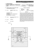 | 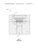 |
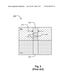 | 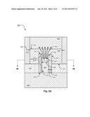 |
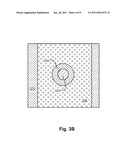 | 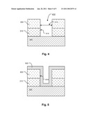 |
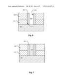 | 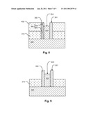 |
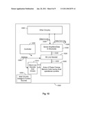 | 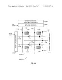 |
| New patent applications in this class: | |
| Date | Title |
|---|---|
| 2022-05-05 | Manufacturing method of resistive memory device |
| 2022-05-05 | Phase-change memory |
| 2016-12-29 | Phase-change memory cell having a compact structure |
| 2016-06-30 | Resistive random access memory and manufacturing method thereof |
| 2016-06-23 | System on chip (soc) based on phase transition and/or phase change material |
| New patent applications from these inventors: | |
| Date | Title |
|---|---|
| 2016-03-17 | Word line repair for 3d vertical channel memory |
| 2015-11-12 | 3d stacked ic device with stepped substack interlayer connectors |
| 2015-09-10 | Contact structure and forming method |
| 2015-07-23 | Twisted array design for high speed vertical channel 3d nand memory |
| 2015-07-23 | Parallelogram cell design for high speed vertical channel 3d nand memory |
| Top Inventors for class "Active solid-state devices (e.g., transistors, solid-state diodes)" | |
| Rank | Inventor's name |
|---|---|
| 1 | Shunpei Yamazaki |
| 2 | Shunpei Yamazaki |
| 3 | Kangguo Cheng |
| 4 | Huilong Zhu |
| 5 | Chen-Hua Yu |