Patent application title: METHOD OF PLATING A WAFER
Inventors:
Yutaka Kasuya (Hiratsuka-Shi, JP)
IPC8 Class: AC25D500FI
USPC Class:
205 89
Class name: Electrolysis: processes, compositions used therein, and methods of preparing the compositions electrolytic coating (process, composition and method of preparing composition) utilizing magnet or magnetic field during coating
Publication date: 2010-02-18
Patent application number: 20100038252
Inventors list |
Agents list |
Assignees list |
List by place |
Classification tree browser |
Top 100 Inventors |
Top 100 Agents |
Top 100 Assignees |
Usenet FAQ Index |
Documents |
Other FAQs |
Patent application title: METHOD OF PLATING A WAFER
Inventors:
YUTAKA KASUYA
Agents:
ROBERTS & ROBERTS, LLP;ATTORNEYS AT LAW
Assignees:
Origin: PRINCETON, NJ US
IPC8 Class: AC25D500FI
USPC Class:
205 89
Patent application number: 20100038252
Abstract:
A plating method for forming a uniform magnetic film in conducting a
plating treatment on a wafer with a magnetic film of, for instance, a
Fe--Co-based alloy. Specifically, the method comprises the steps of
supplying a plating solution through a plating-solution-supply section of
a plating tank to a wafer, which placed on an opening of the plating
tank, and conducting a plating treatment on the wafer while the plating
solution is kept in contact with a plating target surface of the wafer,
wherein the plating solution employed is one forming a magnetic film, and
the plating treatment is done while a magnetic field is applied to the
plating solution in contact with the plating target surface of the wafer.Claims:
1. A method of plating a wafer comprising the steps of supplying a plating
solution through a plating-solution-supply section of a plating tank to a
wafer, which wafer is placed on an opening of the plating tank, and
conducting a plating treating on the wafer while the plating solution is
kept in contact with a plating target surface of the wafer, wherein said
plating solution employed is one forming a magnetic film, and said
plating treatment is done while a magnetic field is applied to the
plating solution in contact with the plating target surface of the wafer.
2. The method of plating a wafer according to claim 1, wherein the step of applying a magnetic field is conducted by arranging at least one magnetic body on an opposite surface of the plating target surface of the wafer.
3. The method of plating a wafer according to claim 1, wherein said magnetic film is either a Fe--Ni-based alloy or a Fe--Co-based alloy.
4. The method of plating a wafer according to claim 2, wherein said magnetic film is either a Fe--Ni-based alloy or a Fe--Co-based alloy.
Description:
BACKGROUND OF THE INVENTION
[0001]1. Technical Field
[0002]The present invention relates to a treatment technology of plating a wafer, and especially to a method of plating a wafer in forming a magnetic film, such as for example a Fe--Ni-based alloy and Fe--Co-based alloy.
[0003]2. Description of the Related Art
[0004]As an apparatus for plating a semiconductor wafer, a cup-shaped plating apparatus has been known conventionally. The cup-shaped plating apparatus supplies a plating solution through a plating-solution-supply section of a plating tank to a wafer, which is placed on an opening of the plating tank, thereby conducting a plating treatment on the wafer while the plating solution being kept in contact with a plating target surface of the wafer.
[0005]The plating apparatus, in which a plating solution is supplied with an upward flow toward a plating target surface of a wafer, allows the plating solution to be in contact with the plating target surface in a manner the solution spreads flowingly in a peripheral direction from a central area of the target surface, so that uniform plating can be advantageously done to a whole plating target surface. This kind of plating apparatus has been widely used as suitable for small lot production and automated plating treatment because it allows wafers being placed onto a wafer supporting section to be changed in series for the purpose of plating treatment, as for example disclosed in Patent Document 1, i.e. Japanese Patent Application Laid-open No. 350185/1999.
[0006]In recent years, semiconductor wafers have been processed to provide various kinds of electronic parts, and thus various types of plating treatments are conducted in tune with many purposes. As a processing technology of a wafer, formation of a magnetic film on a surface of a wafer is in operation. In forming the magnetic film, for example a plating treatment using a Fe--Ni-based alloy known as permalloy or a Fe--Co-based alloy is sometimes performed on a wafer.
[0007]In such a plating treatment where the magnetic film should be formed onto a wafer, more uniform plating film is demanded. Specifically, with the recent development of a processing technology of a fine wiring, an extremely highly accurate plating treatment is demanded to a magnetic film, which is to be applied to a surface of a wafer, and thus a technology enabling more uniform plating film to be formed on a plating target surface of a wafer is demanded. Furthermore, the wafers themselves have been becoming bigger in diameter recently, thereby a plating technology, which forms a uniform magnetic film is desired even if an area of a wafer to be plated is so large.
SUMMARY OF THE INVENTION
[0008]The present invention was made against the above-discussed technical background, and it is an object of the invention in the conventional treatment technology of plating a wafer to provide a plating method, which enables a uniform magnetic film to be formed in conducting a plating treatment on a wafer with a magnetic film such as a Fe--Ni-based alloy, a Fe--Co-based alloy or the like.
[0009]In order to solve the above problem, the present invention defines a plating method for conducting a plating treatment on a wafer, comprising the steps of supplying a plating solution to a wafer, which is placed on an opening of a plating tank, through a plating-solution-supply section of the plating tank, and conducting a plating treatment on a wafer while making the plating solution in contact with a plating target surface of the wafer, characterized by employing a plating solution for forming a magnetic film, and conducting a plating treatment while applying a magnetic field to the plating solution in contact with the plating target surface.
[0010]As a method of applying a magnetic field in the present invention, it is preferable to do by arranging a magnetic body on an opposite surface of the plating target surface of a wafer. More specifically, a magnetic field can be applied in the present invention by arranging permanent magnets or electric magnets on an opposite surface of the plating target surface of a wafer. Arrangement of such magnetic bodies allows a Lorentz force to be wielded to plating ions in the plating solution, thereby achieving an electrodeposited condition not subject to flow of a plating solution and formation of a uniform magnetic film on the plating target surface of a wafer.
[0011]In the present invention, it is preferable that the magnet film is formed with a Fe--Ni-based alloy or a Fe--Co-based alloy. If it is a Fe--Ni-based alloy, a Fe--Ni-based alloy plating solution containing nickel sulphate, nickel chloride, ferrous sulphate, and boric acid can be employed. When such a Fe--Ni based alloy plating solution is employed, it is preferable if the conditions of a plating treatment are 2-10 A/dm2 in terms of current density, 50-65° C. in terms of liquid temperature, and 3.0-3.8 in terms of pH. Alternatively, if it is a Fe--Co-based alloy, the preferable is a Fe--Co-based alloy plating solution containing iron perchlorate (II) hexahydrate, perchlorate cobalt (II) hexahydrate, ammonium chloride, sodium hypophosphite hydrate, and ascorbic acid. When such a Fe--Co-based alloy plating solution is employed, it is preferable if the conditions of a plating treatment are 2-10 A/dm2 in terms of current density, 50-65° C. in terms of liquid temperature, and 3.0-3.8 in terms of pH.
BRIEF DESCRIPTION OF THE DRAWINGS
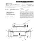
[0012]FIG. 1 is a cross-sectional view of the cup-shaped plating apparatus according to First Embodiment of the present invention;
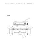
[0013]FIG. 2 is a plane configuration view of a permanent magnet of a wafer depressing machine according to First Embodiment of the present invention; and
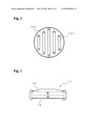
[0014]FIG. 3 is a cross-sectional view of a wafer depressing machine of the cup-shaped plating apparatus according to Second Embodiment of the present invention.
DETAILED DESCRIPTION OF THE INVENTION
[0015]Hereinafter, preferred embodiments of the plating method according to the present invention will be concretely described with reference to the drawings.
First Embodiment
[0016]FIG. 1 is a cross-sectional view, which shows schematically a plating tank of the cup-shaped plating apparatus according to First Embodiment. As shown in FIG. 1, the cup-shaped plating apparatus according to the present embodiment has a wafer-supporting section 2 provided along an upper opening of a plating tank 1, onto which the wafer-supporting section 2 a wafer 3 is to be placed, and a plating treatment is carried out on a plating target surface 4 of the wafer 3. Disposed on the wafer-supporting section 2 are a ring-shaped cathode electrode 5 and a ring-shaped seal packing 6, both being adapted to make contact with a periphery of the wafer 3.
[0017]At the center of a bottom of the plating tank 1, a solution-supply pipe 7 is provided. Below the wafer-supporting section 2, a solution-discharge pipe 8 for discharging a plating solution outside the plating tank 1 is provided. Therefore, a plating solution supplied in upward flow through the solution-supply pipe 7 reaches near the center of the plating target surface 4, and will form a flow as indicated by arrows shown in FIG. 1, which spreads in a direction toward periphery of the wafer 3. Around the solution-supply pipe 7, there is provided an anode electrode 9 in a manner opposed to the plating target surface 4 of the wafer 3.
[0018]Further, above the plating tank 1, there is provided a vertically moveable wafer-depressing machine 11 having permanent magnets 10, which arrange an N pole and S pole in a horizontal direction of a wafer on an upside surface, namely an opposite side of the plating target surface 4 of the wafer. As FIG. 2 shows, permanent magnets 10 have a plurality of rod-like permanent magnets 101 disposed so as to form a magnetic field on the entire area of the plating target surface 4 of the wafer 3. In the case of First Embodiment, it is formed a magnetic field, which provides magnetic field lines advancing from the N pole to S pole in a horizontal direction with respect to the plating target surface 4 of the wafer 3, as indicated by a two-dot broken line in FIG. 1. A thin protective material 12 made of silicon rubber is provided on a downside of the permanent magnets 10 equipped on the wafer-depressing machine 11 in order to prevent the permanent magnets 10 from being damaged by a direct contact with the wafer 3.
Second Embodiment
[0019]Second Embodiment relates to an embodiment where a circular permanent magnet 10' having an essentially identical shape to the plating target surface of a wafer is disposed in place of the rod-like permanent magnet in First Embodiment. In this Second Embodiment, all but the permanent magnet 10' arranged on the wafer-depressing machine 11 are the same as First Embodiment, so that specific showing in the figure and description are omitted. In this Second Embodiment, a magnetic field which provides lines of magnetic force advancing from N-pole to S-pole in a vertical direction in terms of the plating target surface 4 of a wafer 3. See two-doted dash lines in FIG. 3.
[0020]It should be noted that permanent magnets are employed as an example in the above First and Second embodiments, however electric magnets of soft iron for instance can also be employed.
[0021]Lastly, description is made with respect to a result of a plating treatment on a wafer with use of the cup-shaped plating apparatuses of the above First and Second embodiments. The wafer employed in a plating test has a seed metal of Cu provided on the plating target surface thereof, and has a diameter of 200 mm.
[0022]As a plating solution, a Fe--Ni-based alloy plating solution having the following compositions.
TABLE-US-00001 Nickel sulfate 100 g/L Nickel chloride 50 g/L Ferrous sulfate 12 g/L Boric acid 50 g/L pH 3.2 Liquid temperature 60° C. Current density 5 A/dm2 Amount of liquid supplied 4 L/min.
[0023]A plating treatment was performed so that a plating thickness becomes 10 μm.
[0024]In First Embodiment, a total of five rod-like permanent magnets having a size of 10 mm×10 mm in cross section were arranged in a manner illustrated in FIG. 2 and were used. A magnetic flux density of the permanent magnets employed was 40 gauss. In Second Embodiment, a discoid permanent magnet having a diameter of 120 mm and thickness of 10 mm was arranged in a manner so that the N pole should face a wafer as illustrated in FIG. 3 and was used. A magnetic flux density of the permanent magnet employed was also 40 gauss.
[0025]As a result, in the cup-shaped plating apparatuses of First and Second Embodiments, it was found that an entire plating target surface of the wafer had been formed with a magnetic film consisting of a Fe--Ni alloy, which has uniform thickness and good appearance.
User Contributions:
comments("1"); ?> comment_form("1"); ?>Inventors list |
Agents list |
Assignees list |
List by place |
Classification tree browser |
Top 100 Inventors |
Top 100 Agents |
Top 100 Assignees |
Usenet FAQ Index |
Documents |
Other FAQs |
User Contributions:
Comment about this patent or add new information about this topic:
Images included with this patent application:
 |  |
 |
| Similar patent applications: | |
| Date | Title |
|---|---|
| 2009-04-09 | Method of plating metal onto titanium |
| 2009-12-03 | Method of forming plating layer |
| 2012-12-20 | Method of electroplating uniform copper layers |
| 2011-02-17 | Methods of coating magnesium-based substrates |
| 2011-10-20 | Method of operating metal-bromine cells |
| New patent applications in this class: | |
| Date | Title |
|---|---|
| 2015-11-05 | Integrated fluidjet system for stripping, prepping and coating a part |
| 2015-02-26 | Magnetic structure for metal plating control |
| 2014-09-18 | Metal plating apparatus and method using solenoid coil |
| 2013-06-20 | Methods and apparatus for sorting and/or depositing nanotubes |
| 2011-02-24 | Magnetic electro-plating |
| Top Inventors for class "Electrolysis: processes, compositions used therein, and methods of preparing the compositions" | |
| Rank | Inventor's name |
|---|---|
| 1 | Benjamin J. Feldman |
| 2 | Adam Heller |
| 3 | Michael S. Lockard |
| 4 | Fei Mao |
| 5 | Joseph A. Vivolo |