Patent application title: Circuit board assembly
Inventors:
Wei-Cheng Chen (Changhua County, TW)
Cheng-Chao Liao (Taichung City, TW)
IPC8 Class: AH05K111FI
USPC Class:
174263
Class name: With particular conductive connection (e.g., crossover) feedthrough with solder
Publication date: 2009-10-15
Patent application number: 20090255721
includes: a circuit board having opposite first
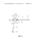
and second surfaces and formed with a first through-hole defined by a
hole-defining wall that extends between and that terminates at the first
and second surfaces and that cooperates with the first and second
surfaces to define first and second turns, respectively, the circuit
board further having an abutting wall that extends between and that
terminates at the first and second surfaces and that cooperates with the
second surface to define a third turn; and an electric wire having a
fixed end that is soldered to the circuit board, extending through the
first through-hole, and passing over the first, second and third turns of
the circuit board so as to form an inflection region between the first
and second turns.Claims:
1. A circuit board assembly comprising:a circuit board having opposite
first and second surfaces and formed with a first through-hole defined by
a hole-defining wall that extends between and that terminates at said
first and second surfaces and that cooperates with said first and second
surfaces to define first and second turns, respectively, said circuit
board further having an abutting wall that extends between and that
terminates at said first and second surfaces, that is spaced apart from
said hole-defining wall, and that cooperates with said second surface to
define a third turn; andan electric wire having a fixed end that is
soldered to said circuit board, extending through said first
through-hole, and passing over said first, second and third turns of said
circuit board so as to form an inflection region between said first and
second turns.
2. The circuit board assembly of claim 1, wherein said electric wire has a first curved segment extending from said fixed end to said inflection region, and a second curved segment extending from said inflection region to said third turn of said circuit board, said first and second curved segments being bent in opposite directions.
3. The circuit board assembly of claim 2, wherein said abutting wall of said circuit board further cooperates with said first surface to define a fourth turn, said electric wire further passing over said fourth turn and further extending repeatedly through said first through-hole in said circuit board so as to form an open loop trained on a portion of said circuit board that extends from said hole-defining wall to said abutting wall.
4. The circuit board assembly of claim 3, wherein said circuit board has a peripheral end that defines said abutting wall.
5. The circuit board assembly of claim 1, wherein said circuit board is further formed with a second through-hole defined by a hole-defining wall that defines said abutting wall of said circuit board.
6. The circuit board assembly of claim 1, wherein said circuit board is further formed with a retaining hole, said fixed end of said electric wire being fixed in said retaining hole.Description:
BACKGROUND OF THE INVENTION
[0001]1. Field of the Invention
[0002]This invention relates to a circuit board assembly, more particularly to a circuit board assembly including a circuit board and an electric wire soldered to the circuit board and formed with an inflection region.
[0003]2. Description of the Related Art
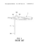
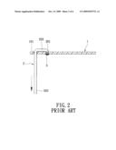
[0004]FIGS. 1 and 2 illustrate a conventional circuit board assembly that includes a circuit board 1 and an electric wire 2 having a fixed end 201 soldered to the circuit board 1 through a solder 3, a curved segment 203 extending from the fixed end 201 to a through-hole 101 in the circuit board 1, and a free segment 202 extending from the curved segment 203. The conventional circuit board assembly is disadvantageous in that the fixed end 201 of the electric wire 2 is likely to be strained when the free segment 202 of the electric wire 2 is pulled by an external force (referring to the arrow in FIG. 2). As a consequence, the fixed end 201 of the electric wire 2 tends to break off from the solder 3 or the solder 3 tends to break after a period of use.
SUMMARY OF THE INVENTION
[0005]Therefore, an object of the present invention is to provide a circuit board assembly that can overcome the aforesaid drawback associated with the prior art.
[0006]According to this invention, a circuit board assembly comprises: a circuit board having opposite first and second surfaces and formed with a first through-hole defined by a hole-defining wall that extends between and that terminates at the first and second surfaces and that cooperates with the first and second surfaces to define first and second turns, respectively, the circuit board further having an abutting wall that extends between and that terminates at the first and second surfaces, that is spaced apart from the hole-defining wall, and that cooperates with the second surface to define a third turn; and an electric wire having a fixed end that is soldered to the circuit board, extending through the first through-hole, and passing over the first, second and third turns of the circuit board so as to form an inflection region between the first and second turns.
BRIEF DESCRIPTION OF THE DRAWINGS
[0007]Other features and advantages of the present invention will become apparent in the following detailed description of the preferred embodiments of the invention, with reference to the accompanying drawings, in which:
[0008]FIG. 1 is a fragmentary perspective view of a conventional circuit board assembly;
[0009]FIG. 2 is a fragmentary partly sectional view of the conventional circuit board assembly;
[0010]FIG. 3 is a fragmentary perspective view of the first preferred embodiment of a circuit board assembly according to this invention;
[0011]FIG. 4 is a fragmentary partly sectional view illustrating a state where an electric wire of the first preferred embodiment is pulled by an external force;
[0012]FIG. 5 is a fragmentary perspective view of the second preferred embodiment of the circuit board assembly according to this invention; and
[0013]FIG. 6 is a fragmentary partly sectional view illustrating a state where the electric wire of the second preferred embodiment is pulled by an external force.
DETAILED DESCRIPTION OF THE PREFERRED EMBODIMENTS
[0014]Before the present invention is described in greater detail with reference to the accompanying preferred embodiments, it should be noted herein that like elements are denoted by the same reference numerals throughout the disclosure.
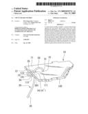
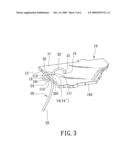
[0015]FIGS. 3 and 4 illustrate the first preferred embodiment of a circuit board assembly according to the present invention. The circuit board assembly includes: a circuit board 10 having opposite first and second surfaces 11, 12 and formed with a first through-hole 14 defined by a hole-defining wall 14' that extends between and that terminates at the first and second surfaces 11, 12 and that cooperates with the first and second surfaces 11, 12 to define first and second turns 111, 112, respectively, the circuit board 10 further having an abutting wall 13 that extends between and that terminates at the first and second surfaces 11, 12, that is spaced apart from the hole-defining wall 14', and that cooperates with the second surface 12 to define a third turn 113; and an electric wire 20 having a fixed end 21 that is soldered to the circuit board 10 through a solder 30, extending through the first through-hole 14, and passing over the first, second and third turns 111, 112, 113 of the circuit board 10 so as to form an inflection region 201, i.e., a transition region where such a change from convex to concave or conversely takes place, between the first and second turns 111, 112.
[0016]In this embodiment, the electric wire 20 has a first curved segment 23 extending from the fixed end 21 to the inflection region 201, and a second curved segment 24 extending from the inflection region 201 to the third turn 113 of the circuit board 10. The first and second curved segments 23, 24 are bent in opposite directions, and are disposed at the first and second surfaces 11, 12, respectively.
[0017]In this embodiment, the abutting wall 13 of the circuit board 10 is defined by a peripheral end 102 of the circuit board 10, and further cooperates with the first surface 11 to define a fourth turn 114. The electric wire 20 further passes over the fourth turn 114, and further extends repeatedly through the first through-hole 14 in the circuit board 10 so as to form an open loop 25 trained on a portion 101 of the circuit board 10 that extends from the hole-defining wall 14' of the first through-hole 14 to the abutting wall 13.
[0018]The circuit board 10 is further formed with a retaining hole 15. The fixed end 21 of the electric wire 20 is fixed in the retaining hole 15 through the solder 30.
[0019]In use, when a free segment 22 of the electric wire 20 is pulled by an external force (referring to the arrow in FIG. 4), the loop 25 will be continuously reduced in size until it is tightly sleeved on the portion 101 of the circuit board 10 (see FIG. 4), thereby preventing the first curved segment 23 of the electric wire 20 from being undesirably strained.
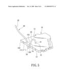
[0020]FIGS. 5 and 6 illustrate the second preferred embodiment of the circuit board assembly according to this invention. The second preferred embodiment differs from the previous embodiment in that the circuit board 10 is further formed with a second through-hole 17 defined by a hole-defining wall 17' that defines the abutting wall 13 of the circuit board 10.
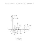
[0021]In use, when an external force is applied to the free segment 22 of the electric wire 20 (see FIG. 6), the electric wire 20 will be tightly trained on a portion 101 of the circuit board 10 that extends from the hole-defining wall 14' of the first through-hole 14 to the hole-defining wall 17' of the second through-hole 17, thereby preventing the fixed end 21 of the electric wire 20 from being undesirably strained.
[0022]By forming the inflection region 201 of the electric wire 20 and by training the electric wire 20 on the portion 101 of the circuit board 10 of the circuit board assembly of this invention, the aforesaid drawback associated with the prior art can be eliminated.
[0023]While the present invention has been described in connection with what are considered the most practical and preferred embodiments, it is understood that this invention is not limited to the disclosed embodiments but is intended to cover various arrangements included within the spirit and scope of the broadest interpretations and equivalent arrangements.
Claims:
1. A circuit board assembly comprising:a circuit board having opposite
first and second surfaces and formed with a first through-hole defined by
a hole-defining wall that extends between and that terminates at said
first and second surfaces and that cooperates with said first and second
surfaces to define first and second turns, respectively, said circuit
board further having an abutting wall that extends between and that
terminates at said first and second surfaces, that is spaced apart from
said hole-defining wall, and that cooperates with said second surface to
define a third turn; andan electric wire having a fixed end that is
soldered to said circuit board, extending through said first
through-hole, and passing over said first, second and third turns of said
circuit board so as to form an inflection region between said first and
second turns.
2. The circuit board assembly of claim 1, wherein said electric wire has a first curved segment extending from said fixed end to said inflection region, and a second curved segment extending from said inflection region to said third turn of said circuit board, said first and second curved segments being bent in opposite directions.
3. The circuit board assembly of claim 2, wherein said abutting wall of said circuit board further cooperates with said first surface to define a fourth turn, said electric wire further passing over said fourth turn and further extending repeatedly through said first through-hole in said circuit board so as to form an open loop trained on a portion of said circuit board that extends from said hole-defining wall to said abutting wall.
4. The circuit board assembly of claim 3, wherein said circuit board has a peripheral end that defines said abutting wall.
5. The circuit board assembly of claim 1, wherein said circuit board is further formed with a second through-hole defined by a hole-defining wall that defines said abutting wall of said circuit board.
6. The circuit board assembly of claim 1, wherein said circuit board is further formed with a retaining hole, said fixed end of said electric wire being fixed in said retaining hole.
Description:
BACKGROUND OF THE INVENTION
[0001]1. Field of the Invention
[0002]This invention relates to a circuit board assembly, more particularly to a circuit board assembly including a circuit board and an electric wire soldered to the circuit board and formed with an inflection region.
[0003]2. Description of the Related Art
[0004]FIGS. 1 and 2 illustrate a conventional circuit board assembly that includes a circuit board 1 and an electric wire 2 having a fixed end 201 soldered to the circuit board 1 through a solder 3, a curved segment 203 extending from the fixed end 201 to a through-hole 101 in the circuit board 1, and a free segment 202 extending from the curved segment 203. The conventional circuit board assembly is disadvantageous in that the fixed end 201 of the electric wire 2 is likely to be strained when the free segment 202 of the electric wire 2 is pulled by an external force (referring to the arrow in FIG. 2). As a consequence, the fixed end 201 of the electric wire 2 tends to break off from the solder 3 or the solder 3 tends to break after a period of use.
SUMMARY OF THE INVENTION
[0005]Therefore, an object of the present invention is to provide a circuit board assembly that can overcome the aforesaid drawback associated with the prior art.
[0006]According to this invention, a circuit board assembly comprises: a circuit board having opposite first and second surfaces and formed with a first through-hole defined by a hole-defining wall that extends between and that terminates at the first and second surfaces and that cooperates with the first and second surfaces to define first and second turns, respectively, the circuit board further having an abutting wall that extends between and that terminates at the first and second surfaces, that is spaced apart from the hole-defining wall, and that cooperates with the second surface to define a third turn; and an electric wire having a fixed end that is soldered to the circuit board, extending through the first through-hole, and passing over the first, second and third turns of the circuit board so as to form an inflection region between the first and second turns.
BRIEF DESCRIPTION OF THE DRAWINGS
[0007]Other features and advantages of the present invention will become apparent in the following detailed description of the preferred embodiments of the invention, with reference to the accompanying drawings, in which:
[0008]FIG. 1 is a fragmentary perspective view of a conventional circuit board assembly;
[0009]FIG. 2 is a fragmentary partly sectional view of the conventional circuit board assembly;
[0010]FIG. 3 is a fragmentary perspective view of the first preferred embodiment of a circuit board assembly according to this invention;
[0011]FIG. 4 is a fragmentary partly sectional view illustrating a state where an electric wire of the first preferred embodiment is pulled by an external force;
[0012]FIG. 5 is a fragmentary perspective view of the second preferred embodiment of the circuit board assembly according to this invention; and
[0013]FIG. 6 is a fragmentary partly sectional view illustrating a state where the electric wire of the second preferred embodiment is pulled by an external force.
DETAILED DESCRIPTION OF THE PREFERRED EMBODIMENTS
[0014]Before the present invention is described in greater detail with reference to the accompanying preferred embodiments, it should be noted herein that like elements are denoted by the same reference numerals throughout the disclosure.
[0015]FIGS. 3 and 4 illustrate the first preferred embodiment of a circuit board assembly according to the present invention. The circuit board assembly includes: a circuit board 10 having opposite first and second surfaces 11, 12 and formed with a first through-hole 14 defined by a hole-defining wall 14' that extends between and that terminates at the first and second surfaces 11, 12 and that cooperates with the first and second surfaces 11, 12 to define first and second turns 111, 112, respectively, the circuit board 10 further having an abutting wall 13 that extends between and that terminates at the first and second surfaces 11, 12, that is spaced apart from the hole-defining wall 14', and that cooperates with the second surface 12 to define a third turn 113; and an electric wire 20 having a fixed end 21 that is soldered to the circuit board 10 through a solder 30, extending through the first through-hole 14, and passing over the first, second and third turns 111, 112, 113 of the circuit board 10 so as to form an inflection region 201, i.e., a transition region where such a change from convex to concave or conversely takes place, between the first and second turns 111, 112.
[0016]In this embodiment, the electric wire 20 has a first curved segment 23 extending from the fixed end 21 to the inflection region 201, and a second curved segment 24 extending from the inflection region 201 to the third turn 113 of the circuit board 10. The first and second curved segments 23, 24 are bent in opposite directions, and are disposed at the first and second surfaces 11, 12, respectively.
[0017]In this embodiment, the abutting wall 13 of the circuit board 10 is defined by a peripheral end 102 of the circuit board 10, and further cooperates with the first surface 11 to define a fourth turn 114. The electric wire 20 further passes over the fourth turn 114, and further extends repeatedly through the first through-hole 14 in the circuit board 10 so as to form an open loop 25 trained on a portion 101 of the circuit board 10 that extends from the hole-defining wall 14' of the first through-hole 14 to the abutting wall 13.
[0018]The circuit board 10 is further formed with a retaining hole 15. The fixed end 21 of the electric wire 20 is fixed in the retaining hole 15 through the solder 30.
[0019]In use, when a free segment 22 of the electric wire 20 is pulled by an external force (referring to the arrow in FIG. 4), the loop 25 will be continuously reduced in size until it is tightly sleeved on the portion 101 of the circuit board 10 (see FIG. 4), thereby preventing the first curved segment 23 of the electric wire 20 from being undesirably strained.
[0020]FIGS. 5 and 6 illustrate the second preferred embodiment of the circuit board assembly according to this invention. The second preferred embodiment differs from the previous embodiment in that the circuit board 10 is further formed with a second through-hole 17 defined by a hole-defining wall 17' that defines the abutting wall 13 of the circuit board 10.
[0021]In use, when an external force is applied to the free segment 22 of the electric wire 20 (see FIG. 6), the electric wire 20 will be tightly trained on a portion 101 of the circuit board 10 that extends from the hole-defining wall 14' of the first through-hole 14 to the hole-defining wall 17' of the second through-hole 17, thereby preventing the fixed end 21 of the electric wire 20 from being undesirably strained.
[0022]By forming the inflection region 201 of the electric wire 20 and by training the electric wire 20 on the portion 101 of the circuit board 10 of the circuit board assembly of this invention, the aforesaid drawback associated with the prior art can be eliminated.
[0023]While the present invention has been described in connection with what are considered the most practical and preferred embodiments, it is understood that this invention is not limited to the disclosed embodiments but is intended to cover various arrangements included within the spirit and scope of the broadest interpretations and equivalent arrangements.
User Contributions:
Comment about this patent or add new information about this topic:
Images included with this patent application:
 |  |
 |  |
 |  |
 |
| Similar patent applications: | |
| Date | Title |
|---|---|
| 2014-04-17 | Rigid flexible circuit board with impedance control |
| 2014-04-17 | Multi-layer type printed circuit board and method of manufacturing the same |
| 2014-04-17 | Flexible circuit board and method for production thereof |
| 2013-11-21 | Bimetal buss bar assembly |
| 2013-12-05 | Underground utility box assembly |
| New patent applications in this class: | |
| Date | Title |
|---|---|
| 2016-02-25 | Dual side solder resist layers for coreless packages and packages with an embedded interconnect bridge and their methods of fabrication |
| 2015-03-05 | Combined printed wiring board and method for manufacturing the same |
| 2015-01-15 | Printed wiring board and electric tool switch provided therewith |
| 2014-10-02 | Printed circuit board solder mounting method and solder mount structure |
| 2014-07-17 | Through mold via relief gutter on molded laser package (mlp) packages |
| New patent applications from these inventors: | |
| Date | Title |
|---|---|
| 2008-10-23 | Resealable box |
| Top Inventors for class "Electricity: conductors and insulators" | |
| Rank | Inventor's name |
|---|---|
| 1 | Douglas B. Gundel |
| 2 | Shou-Kuo Hsu |
| 3 | Michimasa Takahashi |
| 4 | Hideyuki Kikuchi |
| 5 | Tsung-Yuan Chen |