Patent application title: LOW VT DEPENDENCY RC OSCILLATOR
Inventors:
Tomer Shaul Elran (Petah Tikva, IL)
IPC8 Class: AH03K3011FI
USPC Class:
327291
Class name: Miscellaneous active electrical nonlinear devices, circuits, and systems signal converting, shaping, or generating clock or pulse waveform generating
Publication date: 2009-06-25
Patent application number: 20090160521
o current sources that have the same temperature
and VDD dependency so they generate the same current in changing
conditions. Therefore, there is very low VT dependency. The resistor and
fringe capacitor temperature coefficient are very low and opposite so
they compensate for each other. A comparator with a short period of
operation also minimizes VT dependency.Claims:
1. An oscillator comprising:a first current source, the first current
source characterized by:a first temperature dependency;a first input
voltage dependency;a second current source, the second current source
characterized by:a second temperature dependency;a second input voltage
dependency;the first temperature dependency equal to the second
temperature dependency, the first input voltage dependency equal to the
second input voltage dependency;a reference voltage generated by applying
a current of the first current source to a resistor;a capacitor coupled
to an output of the second current source; anda comparator comprising an
output and configured to change the output when the capacitor voltage
reaches the reference voltage.
2. The oscillator of claim 1, wherein the change in resistance with temperature of the resistor is substantially equal in magnitude to the change in capacitance of the capacitor with temperature.
3. The oscillator of claim 1, wherein the change in resistance with temperature of the resistor is opposite in sign to the change in capacitance of the capacitor with temperature.
4. The oscillator of claim 1, further comprising logical circuitry coupled to the comparator and configured to discharge the capacitor.
5. The oscillator of claim 1, wherein the oscillator produces a signal in the range of approximately 50-200 MHz.
6. A method of providing a clock signal in a memory device, the method comprising:providing a first and a second current source, the first and second current source having the same VGS;applying a current of the first current source to a resistor and generating a reference voltage;applying a current of the second current source to a capacitor and charging the capacitor; andwhen the capacitor voltage reaches the reference voltage generating the clock signal.
7. The method of claim 6 wherein the change in resistance/change in temperature of the first current source is approximately equal in magnitude but opposite in value to the change in capacitance/change in temperature of the second current source.
8. The method of claim 6 wherein the first current source has a first temperature dependency, and wherein the second current source has a second current dependency, the first and second current dependency substantially equal.
9. The method of claim 6 wherein the first current source has a first temperature dependency, and wherein the second current source has a second current dependency, the first and second current dependency substantially equal.
10. The method of claim 6, wherein the clock signal is provided in the range of approximately 50-200 MHz.
11. The method of claim 6, further comprising disabling the clock signal when the memory device is not active, and wherein an associated leakage current of the circuitry generating the clock signal is less than 0.1 microamperes.Description:
BACKGROUND OF THE INVENTION
[0001]The present application relates to oscillators, and the use of oscillators in generating a system clock.
[0002]Oscillators and the circuit components employed in oscillators are dependent upon the environment they operate in. For example, oscillator signals fluctuate with temperature. It is desirable to minimize such voltage-temperature ("VT") fluctuation.
[0003]Prior ways to address the temperature induced fluctuations include:
1. Adding a compensation device (usually current compensation) to fix the temperature dependency.2. Using temperature trimming calibrated only one time during sort (after the accurate temperature curve was found in lab tests).3. Using a voltage regulator to correct the voltage dependency.
[0004]All the solutions above increase the circuit complexity, expand its size, reduce the yield in production or make the sorting process longer and more expensive. Furthermore, even after such solutions were incorporated, VT dependency is still unacceptably high, e.g. +/-7% at 100 MHz.
SUMMARY OF THE INVENTION
[0005]An oscillator utilizes two current sources that have the same temperature and VDD dependency so they generate the same current in changing conditions. Therefore, there is very low VT dependency. The resistor and fringe capacitor temperature coefficient are very low and opposite so they compensate for each other. A comparator with a short period of operation also minimizes VT dependency.
[0006]One aspect of an embodiment of the invention relates to a method of providing a clock signal in a memory device. The method comprises providing a first and a second current source, the first and second current source having the same VGS, applying a current of the first current source to a resistor and generating a reference voltage, applying a current of the second current source to a capacitor and charging the capacitor, and when the capacitor voltage reaches the reference voltage the comparator output flips, discharging the capacitor and generating the clock signal.
BRIEF DESCRIPTION OF THE DRAWINGS
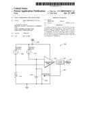
[0007]FIG. 1 is a block diagram of oscillator 100.
[0008]FIG. 2 is a graph of capacitor charging, discharging, and reset over time.
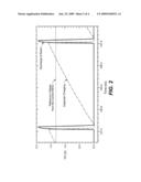
[0009]FIG. 3 is a graph of current consumption and transient response.
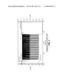
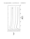
[0010]FIG. 4 is a graph of frequency over time at different temperatures.
DETAILED DESCRIPTION OF THE PREFERRED EMBODIMENTS
[0011]FIG. 1 illustrates oscillator 100, which may be used as an on chip internal oscillator. Oscillator 100 may be employed in many different environments, and in certain embodiments is employed to generate a system clock for use in a flash memory storage device or part of a larger system incorporating such a device, such as a music player, digital camera, or other computing device.
[0012]An input voltage (VDD) 102 supplies current source 106 and current source 110 with the same input voltage. Current sources 106 and 110 are "mirrored." That is to say that they have the same or similar operating characteristics, and are preferably identical. In particular, they preferably employ the same internal voltage gate and have the same gate-source voltage VGS. The output of current source 106 passes to resistor 114 and operational amplifier 122. The output of current source 100 passes to capacitor 118 and operational amplifier 122. Operational amplifier 122 may also be referred to as a comparator. Note the circuit interconnections to both the inputs (V.sub.+, V.sub.-) as well as the power supply terminals (VS+, VS-) of operational amplifier 122. The output of comparator 122 is connected to logical circuitry 130, which is connected to switch 126 via line 128. The output 134 of oscillator 100 is a square wave signal.
[0013]The current applied to resistor 114 generates a reference voltage and the current applied to capacitor 118 charges capacitor 118. When the capacitor 118 voltage reaches the reference voltage (from resistor 114) the comparator output flips and using logic block 130 triggers the capacitor 118 to discharge via line 128 and switch 126, thus generating the clock signal and setting the oscillator for another period.
[0014]The two current sources have the same temperature and VDD dependency so they generate the same current in changing conditions. Therefore, there is very low VT dependency. The resistor and fringe capacitor temperature coefficient are very low and opposite so they compensate for each other. The comparator is very fast so its error contribution for the VT dependency is also low, as can be seen in the equations below.
I*R=(I*tRC)/C→tRC=R*C
R=r0*(1+(dr/dtemp)*(temp0-temp))
C=c0*(1+(dc/dtemp)*(temp0-temp))
(dr/dtemp)˜-(dc/dtemp),x=(dr/dtemp)*(temp0-temp)<3%
tRC=R*C=(r0(1+x))*(c0(1-x))=r0*c0(1-X 2)˜r0*c0
tperiod=tRC+tcomparator
[0015]The oscillator has many advantages compared to previous designs. The oscillator has very low VT dependency. Early embodiments of the present invention exhibited around: +/-3%, whereas further refined embodiments have exhibited less than +/-1% with additional reductions in VT dependency expected. The oscillator has process trimming with 0.5 MHz resolution, and low current consumption as compared to previous designs. Preferred embodiments, for example have current consumption of less than 3 mA. In disable mode the oscillator has very low current consumption, or leakage current, so it is very suitable for portable and battery driven devices because it will not drain the battery when the device is not in use. The oscillator also occupies a very small area of about 0.02 mm2. Thus, as compared to prior designs with larger circuits and high VT dependency, the present invention produces more economical and reliable electronic devices, especially when those devices are subjected to temperature swings, as is often the case with portable electronics such as memory cards, digital cameras, and music players etc.
[0016]FIGS. 2-4 illustrate the rapid transient response, low VT dependency, and low current consumption of oscillator embodiments according to the present invention. FIG. 2 is a graph illustrating capacitor charging, discharge, and reset over time. FIG. 3 is a graph of current consumption and transient response. Note the low current consumption when in enable mode and the low leakage current when in disable mode. FIG. 4 is a graph of frequency over time at different temperatures. Note the consistency in operation at different temperatures.
[0017]The following table illustrates some operating characteristics of one implementation or embodiment of the present invention. The table is provided for exemplary purposes and is not intended to limit the invention, as defined by the appended claims, in any way.
Electrical Characteristics:
Vdd33=2.7-3.6V Temperature: -40<Tj<125 C
TABLE-US-00001 [0018]Parameter symbol conditions min typ max units Power supply VDD33 Operating conditions 2.7 3.3 3.6 V Vop - min Vop 2.6 V operation power supply voltage Temp Temp_trim<6:0> Positive temp compensation 0000000 0111111 b Trimming negative temp compensation 1000000 1111111 Frequency Frequency_cal<10:0> Process calibration& Fine 000h 7FFh b calibration tuning Minimum Frequency_cal<10:0> = 00h 25 MHz Frequency Maximum Frequency_cal<10:0> = 7FFh 80 MHz frequency Frequency 0.03 0.04 0.05 MHz resolution Duty Cycle 40 50 60 % Temp After process & -40 < Tj < 125 -0.2 0.2 % Dependency temp calibration VDD 2.7 < VDD < 3.6 -0.05 0.05 % Dependency Total peak Clean VDD 0.5 % Jitter: 3 sigma Total peak VDD33 ± 500 mv ripple/ 1 % Jitter: 3sigma 10 Hz-10 MHz) Start up time To 99% of final value 2 usec from To 99.9% of final value 400 Power up or (temp compensation circuit disable startup takes time when ss, -40 C.) Stabilization 0.5 usec time from change of Calibration to 0.5% of final frequency Operating Iop 0.8 1 1.5 mA Current Leakage Ileak En = 0 0.1 uA current Area 0.24 mm{circumflex over ( )}2 Max load on 100 fF internal clock
Claims:
1. An oscillator comprising:a first current source, the first current
source characterized by:a first temperature dependency;a first input
voltage dependency;a second current source, the second current source
characterized by:a second temperature dependency;a second input voltage
dependency;the first temperature dependency equal to the second
temperature dependency, the first input voltage dependency equal to the
second input voltage dependency;a reference voltage generated by applying
a current of the first current source to a resistor;a capacitor coupled
to an output of the second current source; anda comparator comprising an
output and configured to change the output when the capacitor voltage
reaches the reference voltage.
2. The oscillator of claim 1, wherein the change in resistance with temperature of the resistor is substantially equal in magnitude to the change in capacitance of the capacitor with temperature.
3. The oscillator of claim 1, wherein the change in resistance with temperature of the resistor is opposite in sign to the change in capacitance of the capacitor with temperature.
4. The oscillator of claim 1, further comprising logical circuitry coupled to the comparator and configured to discharge the capacitor.
5. The oscillator of claim 1, wherein the oscillator produces a signal in the range of approximately 50-200 MHz.
6. A method of providing a clock signal in a memory device, the method comprising:providing a first and a second current source, the first and second current source having the same VGS;applying a current of the first current source to a resistor and generating a reference voltage;applying a current of the second current source to a capacitor and charging the capacitor; andwhen the capacitor voltage reaches the reference voltage generating the clock signal.
7. The method of claim 6 wherein the change in resistance/change in temperature of the first current source is approximately equal in magnitude but opposite in value to the change in capacitance/change in temperature of the second current source.
8. The method of claim 6 wherein the first current source has a first temperature dependency, and wherein the second current source has a second current dependency, the first and second current dependency substantially equal.
9. The method of claim 6 wherein the first current source has a first temperature dependency, and wherein the second current source has a second current dependency, the first and second current dependency substantially equal.
10. The method of claim 6, wherein the clock signal is provided in the range of approximately 50-200 MHz.
11. The method of claim 6, further comprising disabling the clock signal when the memory device is not active, and wherein an associated leakage current of the circuitry generating the clock signal is less than 0.1 microamperes.
Description:
BACKGROUND OF THE INVENTION
[0001]The present application relates to oscillators, and the use of oscillators in generating a system clock.
[0002]Oscillators and the circuit components employed in oscillators are dependent upon the environment they operate in. For example, oscillator signals fluctuate with temperature. It is desirable to minimize such voltage-temperature ("VT") fluctuation.
[0003]Prior ways to address the temperature induced fluctuations include:
1. Adding a compensation device (usually current compensation) to fix the temperature dependency.2. Using temperature trimming calibrated only one time during sort (after the accurate temperature curve was found in lab tests).3. Using a voltage regulator to correct the voltage dependency.
[0004]All the solutions above increase the circuit complexity, expand its size, reduce the yield in production or make the sorting process longer and more expensive. Furthermore, even after such solutions were incorporated, VT dependency is still unacceptably high, e.g. +/-7% at 100 MHz.
SUMMARY OF THE INVENTION
[0005]An oscillator utilizes two current sources that have the same temperature and VDD dependency so they generate the same current in changing conditions. Therefore, there is very low VT dependency. The resistor and fringe capacitor temperature coefficient are very low and opposite so they compensate for each other. A comparator with a short period of operation also minimizes VT dependency.
[0006]One aspect of an embodiment of the invention relates to a method of providing a clock signal in a memory device. The method comprises providing a first and a second current source, the first and second current source having the same VGS, applying a current of the first current source to a resistor and generating a reference voltage, applying a current of the second current source to a capacitor and charging the capacitor, and when the capacitor voltage reaches the reference voltage the comparator output flips, discharging the capacitor and generating the clock signal.
BRIEF DESCRIPTION OF THE DRAWINGS
[0007]FIG. 1 is a block diagram of oscillator 100.
[0008]FIG. 2 is a graph of capacitor charging, discharging, and reset over time.
[0009]FIG. 3 is a graph of current consumption and transient response.
[0010]FIG. 4 is a graph of frequency over time at different temperatures.
DETAILED DESCRIPTION OF THE PREFERRED EMBODIMENTS
[0011]FIG. 1 illustrates oscillator 100, which may be used as an on chip internal oscillator. Oscillator 100 may be employed in many different environments, and in certain embodiments is employed to generate a system clock for use in a flash memory storage device or part of a larger system incorporating such a device, such as a music player, digital camera, or other computing device.
[0012]An input voltage (VDD) 102 supplies current source 106 and current source 110 with the same input voltage. Current sources 106 and 110 are "mirrored." That is to say that they have the same or similar operating characteristics, and are preferably identical. In particular, they preferably employ the same internal voltage gate and have the same gate-source voltage VGS. The output of current source 106 passes to resistor 114 and operational amplifier 122. The output of current source 100 passes to capacitor 118 and operational amplifier 122. Operational amplifier 122 may also be referred to as a comparator. Note the circuit interconnections to both the inputs (V.sub.+, V.sub.-) as well as the power supply terminals (VS+, VS-) of operational amplifier 122. The output of comparator 122 is connected to logical circuitry 130, which is connected to switch 126 via line 128. The output 134 of oscillator 100 is a square wave signal.
[0013]The current applied to resistor 114 generates a reference voltage and the current applied to capacitor 118 charges capacitor 118. When the capacitor 118 voltage reaches the reference voltage (from resistor 114) the comparator output flips and using logic block 130 triggers the capacitor 118 to discharge via line 128 and switch 126, thus generating the clock signal and setting the oscillator for another period.
[0014]The two current sources have the same temperature and VDD dependency so they generate the same current in changing conditions. Therefore, there is very low VT dependency. The resistor and fringe capacitor temperature coefficient are very low and opposite so they compensate for each other. The comparator is very fast so its error contribution for the VT dependency is also low, as can be seen in the equations below.
I*R=(I*tRC)/C→tRC=R*C
R=r0*(1+(dr/dtemp)*(temp0-temp))
C=c0*(1+(dc/dtemp)*(temp0-temp))
(dr/dtemp)˜-(dc/dtemp),x=(dr/dtemp)*(temp0-temp)<3%
tRC=R*C=(r0(1+x))*(c0(1-x))=r0*c0(1-X 2)˜r0*c0
tperiod=tRC+tcomparator
[0015]The oscillator has many advantages compared to previous designs. The oscillator has very low VT dependency. Early embodiments of the present invention exhibited around: +/-3%, whereas further refined embodiments have exhibited less than +/-1% with additional reductions in VT dependency expected. The oscillator has process trimming with 0.5 MHz resolution, and low current consumption as compared to previous designs. Preferred embodiments, for example have current consumption of less than 3 mA. In disable mode the oscillator has very low current consumption, or leakage current, so it is very suitable for portable and battery driven devices because it will not drain the battery when the device is not in use. The oscillator also occupies a very small area of about 0.02 mm2. Thus, as compared to prior designs with larger circuits and high VT dependency, the present invention produces more economical and reliable electronic devices, especially when those devices are subjected to temperature swings, as is often the case with portable electronics such as memory cards, digital cameras, and music players etc.
[0016]FIGS. 2-4 illustrate the rapid transient response, low VT dependency, and low current consumption of oscillator embodiments according to the present invention. FIG. 2 is a graph illustrating capacitor charging, discharge, and reset over time. FIG. 3 is a graph of current consumption and transient response. Note the low current consumption when in enable mode and the low leakage current when in disable mode. FIG. 4 is a graph of frequency over time at different temperatures. Note the consistency in operation at different temperatures.
[0017]The following table illustrates some operating characteristics of one implementation or embodiment of the present invention. The table is provided for exemplary purposes and is not intended to limit the invention, as defined by the appended claims, in any way.
Electrical Characteristics:
Vdd33=2.7-3.6V Temperature: -40<Tj<125 C
TABLE-US-00001 [0018]Parameter symbol conditions min typ max units Power supply VDD33 Operating conditions 2.7 3.3 3.6 V Vop - min Vop 2.6 V operation power supply voltage Temp Temp_trim<6:0> Positive temp compensation 0000000 0111111 b Trimming negative temp compensation 1000000 1111111 Frequency Frequency_cal<10:0> Process calibration& Fine 000h 7FFh b calibration tuning Minimum Frequency_cal<10:0> = 00h 25 MHz Frequency Maximum Frequency_cal<10:0> = 7FFh 80 MHz frequency Frequency 0.03 0.04 0.05 MHz resolution Duty Cycle 40 50 60 % Temp After process & -40 < Tj < 125 -0.2 0.2 % Dependency temp calibration VDD 2.7 < VDD < 3.6 -0.05 0.05 % Dependency Total peak Clean VDD 0.5 % Jitter: 3 sigma Total peak VDD33 ± 500 mv ripple/ 1 % Jitter: 3sigma 10 Hz-10 MHz) Start up time To 99% of final value 2 usec from To 99.9% of final value 400 Power up or (temp compensation circuit disable startup takes time when ss, -40 C.) Stabilization 0.5 usec time from change of Calibration to 0.5% of final frequency Operating Iop 0.8 1 1.5 mA Current Leakage Ileak En = 0 0.1 uA current Area 0.24 mm{circumflex over ( )}2 Max load on 100 fF internal clock
User Contributions:
Comment about this patent or add new information about this topic:
| People who visited this patent also read: | |
| Patent application number | Title |
|---|---|
| 20190175436 | FOLDABLE ARM FOR WALKER |
| 20190175435 | MUSCULAR STRENGTH ASSISTING APPARATUS |
| 20190175434 | RECIPROCATING-HIT TREATMENT INSTRUMENT |
| 20190175433 | HEADSET SYSTEM |
| 20190175432 | Limb Irrigation Pan Device |
Images included with this patent application:
 |  |
 |  |
 |  |
 |
| Similar patent applications: | |
| Date | Title |
|---|---|
| 2011-12-29 | Signal generator with output frequency greater than the oscillator frequency |
| 2010-09-09 | Reduced line driver output dependency on process, voltage, and temperature variations |
| 2011-08-18 | Line driver with reduced dependency on process, voltage, and temperature |
| 2011-06-30 | Low noise fractional divider using a multiphase oscillator |
| 2011-03-17 | Delay-locked loop having a delay independent of input signal duty cycle variation |
| New patent applications in this class: | |
| Date | Title |
|---|---|
| 2022-05-05 | Software-defined pulse orchestration platform |
| 2016-06-30 | Spread-spectrum clock generation circuit, integrated circuit and apparatus therefor |
| 2016-06-09 | Signal input circuit and operating method thereof |
| 2016-06-09 | Signal comparison apparatus and method of controlling same |
| 2016-04-14 | Implementing broadband resonator for resonant clock distribution |
| New patent applications from these inventors: | |
| Date | Title |
|---|---|
| 2013-09-05 | Programmable slew rate power switch |
| 2010-11-18 | Transient load voltage regulator |
| Top Inventors for class "Miscellaneous active electrical nonlinear devices, circuits, and systems" | |
| Rank | Inventor's name |
|---|---|
| 1 | Yantao Ma |
| 2 | Feng Lin |
| 3 | Ming-Chieh Huang |
| 4 | Yong-Ju Kim |
| 5 | Chan-Hong Chern |