Patent application title: METHOD OF FABRICATING A MASK FOR A SEMICONDUCTOR DEVICE
Inventors:
Sung Hyun Oh (Cheongju-Si, KR)
Assignees:
Hynix Semiconductor Inc.
IPC8 Class: AG03F100FI
USPC Class:
430 5
Class name: Radiation imagery chemistry: process, composition, or product thereof radiation modifying product or process of making radiation mask
Publication date: 2008-11-13
Patent application number: 20080280213
g a mask for a semiconductor device, a phase
shift layer and a light blocking layer are formed on a transparent
substrate. The light blocking layer is patterned to form light blocking
patterns which partially expose a surface of the phase shift layer. An
extension defect or a bridge defect is detected. A photoresist layer,
which does not react to light, is formed on a resulting structure
including the detected defect. The extension defect is removed by
performing a repair process on the light blocking patterns. The bridge
defect is removed by etching using the light blocking patterns as a mask.Claims:
1. A method of fabricating a mask for a semiconductor device, the method
comprising:forming a phase shift layer and a light blocking layer over a
transparent substrate;forming a light blocking patterns by patterning the
light blocking layer, wherein light blocking patterns partially expose a
surface of the phase shift layer;detecting an extension defect which is
generated when the light blocking patterns are formed;forming a
photoresist layer over a resulting structure of the detected extension
defect and the light blocking layer, wherein the photoresist layer does
not react to light;exposing the light blocking patterns by performing a
development process on the photoresist layer;removing the extension
defect by performing a repair process on the light blocking patterns;
andremoving the photoresist layer.
2. The method according to claim 1, wherein the phase shift layer includes a molybdenum compound.
3. The method according to claim 1, wherein the light blocking layer includes a chrome compound.
4. The method according to claim 1, wherein removing the extension defect comprises irradiating a laser beam onto the extension defect.
5. The method according to claim 1, wherein the transparent substrate includes quartz.
6. The method according to claim 1, wherein the photoresist layer dissolves in a developing solution at a constant dissolution rate during the development process.
7. The method of claim 1, wherein the photoresist layer does not include a photoacid generator.
8. A method of fabricating a mask for a semiconductor device, the method comprising:forming a phase shift layer and a light blocking layer over a transparent substrate;forming light blocking patterns by patterning the light blocking layer, wherein the light blocking patterns partially expose a surface of the phase shift layer;forming phase shift patterns using the light blocking patterns;detecting a bridge defect which is generated when the phase shift patterns are formed;forming a photoresist layer over a resulting structure of the detected bridge defect and the exposed layers, wherein the photoresist layer does not react to light;exposing the bridge defect by performing a development process on the photoresist layer;etching the exposed bridge defect using the light blocking patterns as a mask; andremoving the photoresist layer.
9. The method according to claim 8, wherein the phase shift layer includes a molybdenum compound.
10. The method according to claim 8, wherein the light blocking layer includes a chrome compound.
11. The method according to claim 8, wherein the transparent substrate includes quartz.
12. The method according to claim 8, wherein the photoresist layer dissolves in a developing solution at a constant dissolution rate during the development process.
13. The method according to claim 8, wherein the photoresist layer does not include a photoacid generator.Description:
CROSS-REFERENCES TO RELATED APPLICATION
[0001]The priority of Korean application number 10-2007-0045793, filed on May 11, 2007, which is incorporated by reference in its entirety, is claimed.
BACKGROUND OF THE INVENTION
[0002]The invention relates to a semiconductor device and, more particularly, to a method of fabricating a mask for a semiconductor device capable of easily correcting a mask defect.
[0003]Several photolithography processes are performed to form patterns on a semiconductor substrate in a process of manufacturing a semiconductor device. The photolithography process requires a mask which has fine patterns to form the patterns on the substrate. However, when such a mask is fabricated, a defect sometimes occurs on the mask so that the mask is rejected.
[0004]A common reason for rejection of the mask is an occurrence of defects such as a bridge that causes adjacent patterns to be connected to each other in a process of forming the patterns on the mask. Another common reason for rejection of the mask is that a size of the patterns increases due to residue accumulation in the pattern. Usually, the defect is corrected by inspecting the mask after fabricating the mask and performing a repair process for a detected defect. The repair process is performed by irradiating a laser beam onto the mask defect.
[0005]However, during such a repair process, the laser beam may cause damage to a material formed on the mask so that a phase or transmittance of the patterns is adversely affected. Specifically, when a large number of defects exist on the mask such that the repair process becomes tedious, mask quality cannot be guaranteed after performing the repair process. Also, the yield of the semiconductor devices in the mask fabricating process cannot be improved because the repair process is time consuming.
[0006]Accordingly, a method for effectively correcting mask defects without requiring a time consuming repair process is desired.
SUMMARY OF THE INVENTION
[0007]In one embodiment of the invention, a method of fabricating a mask for a semiconductor device includes forming a phase shift layer and a light blocking layer on a transparent substrate. Light blocking patterns are formed which partially expose a surface of the phase shift layer by patterning the light blocking layer. An extension defect is detected. The extension defect is generated when the light blocking patterns are formed. A photoresist layer is formed on a resulting structure of the detected extension defect and the light blocking layer. The photoresist layer does not react to light. The light blocking patterns are exposed by a development process performed on the photoresist layer. The extension defect is removed by performing a repair process on the light blocking patterns. The photoresist layer is then removed.
[0008]The phase shift layer includes a molybdenum compound and the light blocking layer includes a chrome compound. The repair process removes the extension defect by irradiating a laser beam onto the defect.
[0009]In another embodiment of the invention, a method of fabricating a mask for a semiconductor device includes forming a phase shift layer and a light blocking layer on a transparent substrate. Light blocking patterns are formed which partially expose a surface of the phase shift layer by patterning the light blocking layer. Phase shift patterns are formed using the light blocking patterns. A bridge defect is detected. The bridge defect is generated when the phase shift patterns are formed. A photoresist layer is formed on a resulting structure of the detected bridge defect and the exposed layers. The photoresist layer does not react to light. The bridge defect is exposed by performing a development process on the photoresist layer. The exposed bridge defect is etched using the light blocking patterns and the phase shift patterns as a mask. The photoresist layer is then removed.
BRIEF DESCRIPTION OF THE DRAWINGS
[0010]The above and other objects, features and advantages of the invention will be more apparent from the following detailed description taken in conjunction with the accompanying drawings, in which:
[0011]FIGS. 1 to 12 are cross-sectional views illustrating a method of fabricating a mask for a semiconductor device according to the present invention.
DESCRIPTION OF SPECIFIC EMBODIMENTS
[0012]FIGS. 1 to 12 are cross-sectional views illustrating a method of fabricating a mask for a semiconductor device, according to an embodiment of the invention.
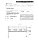
[0013]Referring to FIG. 1, a phase shift layer 102 and a light blocking layer 104 are deposited on a transparent substrate 100. The transparent substrate 100 is made of transparent material such as quartz. The phase shift layer 102 is made of a material that shifts a phase of light in a subsequent exposure process. In one embodiment, the phase shift layer 102 includes a molybdenum compound, for example, molybdenum silicon nitride (MoSiON). The light blocking layer 104 may be a chrome (Cr) film. Photoresist patterns 106 that form a mask pattern area are formed on the light blocking layer 104 by depositing and patterning a photoresist material.
[0014]Referring to FIG. 2, light blocking patterns 108 are formed by etching the light blocking layer 104 using the photoresist patterns 106 as a mask. The light blocking patterns 108 partially expose a surface of the phase shift layer 102. Thereafter, the photoresist patterns 106 are removed using a strip process.
[0015]During the process of forming the light blocking patterns 108, an extension defect 109, in which a pattern size is unexpectedly extended as much as a distance "b," may occur. The extension defect 109 affects a subsequent etching process of the phase shift layer 102 so that it becomes difficult to form an accurate pattern. Therefore, a process may be required to remove the extension defect 109.
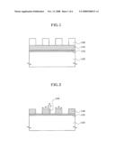
[0016]Referring to FIG. 3, a first photoresist layer 110 is deposited on the exposed phase shift layer 102 and the light blocking patterns 108. The first photoresist layer 110 does not include a photoacid generator.
[0017]The photoresist layer is made of a photosensitive material used in an exposure process. The photoresist layer exhibits properties which change in response to a specific wavelength of light. Specifically, the photoresist material has a high molecular composition of which a chemical structure change happens rapidly due to light irradiation so that property changes occur in the solubility for any solvent, as well as property changes in coloring and hardening. Usually, the photoresist material includes a photoacid generator, a resin, a solvent and an additive. The photoacid generator generates an acid when receiving light. This acid is activated during a post-exposure baking process and operates as a catalyst for a reaction of separating a dissolution inhibitor from the resin. The resin to which the dissolution inhibitor adheres does not dissolve in a developing solution in a subsequent development process. The resin which does not include the dissolution inhibitor dissolves well. Thus, an unexposed area remains as a photoresist pattern. The solvent is used for a dissolution effect and for improved coating. The solvent also improves uniformity when coating the photoresist material. The additive is used for improved leveling, adhesion and storage stability.
[0018]When the photoacid generator is not included in the photoresist material, the first photoresist layer 110 does not react to light during an exposure process. Furthermore, the first photoresist layer 110 that does not include the photoacid generator has a constant dissolution rate for a developing solution in a subsequent development process.
[0019]Referring to FIG. 4, a development process is performed on the first photoresist layer 110 without light exposure, thereby exposing surfaces of the light blocking patterns 108. The first photoresist layer 110 dissolves in a developing solution at a constant dissolution rate. The development process is performed until the surfaces of the light blocking patterns 108 are exposed.
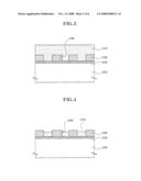
[0020]Referring to FIG. 5, a defect inspection is performed on the transparent substrate 100 and the extension defect 109 generated in the light blocking pattern 108 is detected. A repair process for removing the detected extension defect 109 is then performed. The extension defect 109 can be removed by irradiating a laser beam onto the defect. Since the first photoresist layer 110 covers the phase shift layer 102 exposed between the light blocking patterns 108, the first photoresist layer 110 operates as a protective layer to prevent the phase shift layer 102 and the transparent substrate 100 from being damaged during the repair process.
[0021]In the conventional method, the repair process is conducted for a detected defect after forming a mask and performing a defect inspection on the mask. In such a case, damage may occur on a pattern formed on the mask during the repair process. Damage occurring on the pattern adversely affects a phase or transmittance of the pattern. Therefore, in one embodiment of the present invention, a defect inspection and a repair process are performed after the light blocking patterns 108 and the first photoresist layer 110 are formed. The first photoresist layer 110 prevents the phase shift layer 102 and the transparent substrate 100 from being damaged during the repair process.
[0022]Referring to FIG. 6, a strip process is performed on the transparent substrate 100 to remove the first photoresist layer 110. Subsequently, a cleaning process for removing residue and eliminating contamination is performed. Thus, a surface of the phase shift layer 102 is exposed.
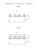
[0023]Referring to FIG. 7, a first etching is performed using the light blocking patterns 108 as a mask to form phase shift patterns 112. However, during the process of forming the phase shift patterns 112, a bridge defect 114 may occur. The bridge defect 114 results from an improper etching of the phase shift layer so that adjacent patterns are connected to each other. The bridge defect 114 can be removed by a repair process. However, when a large number of defects exist on a mask, the repair process becomes tedious and mask quality cannot be guaranteed. Also, if the repair process becomes overly time consuming, the yield of the semiconductor devices in the mask fabricating process cannot be improved. Accordingly, a process is required to remove the bridge defect 114 without performing a repair process.
[0024]Referring to FIG. 8, a second photoresist layer 116 is coated on the light blocking patterns 108, the phase shift patterns 112 and the transparent substrate 100. The second photoresist layer 116 does not include a photoacid generator. As described above, the photoacid generator is a catalyst for a reaction with light. Thus, the second photoresist layer 116 does not react to light in an exposure process and has a constant dissolution rate for a developing solution in a subsequent development process.
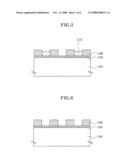
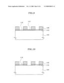
[0025]Referring to FIG. 9, a development process is performed on the second photoresist layer 116 without light exposure. The second photoresist layer 116 dissolves in a developing solution at a constant dissolution rate. In one embodiment, the development process is performed until the bridge defect 114 is exposed.
[0026]Referring to FIG. 10, a second etching using the light blocking patterns 108 as an etching mask is performed to form the phase shift patterns 112. Since the second photoresist layer 116 covers the transparent substrate 100, the transparent substrate 100 is prevented from being damaged during the etching process. Although many bridge defects 114 may be formed on the mask, all of the bridge defects may be removed by the second etching process using the second photoresist layer 116 as a mask. Thus, a repair process need not be performed.
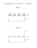
[0027]Referring to FIG. 11, a strip process is performed on the transparent substrate 100 so that the second photoresist layer 116 is removed. Subsequently, a cleaning process for removing residue and eliminating contamination is performed. Thus, a surface of the transparent substrate 100 is partially exposed.
[0028]Referring to FIG. 12, a mask 118 is formed by removing the light blocking patterns 108.
[0029]The method of fabricating a mask for a semiconductor device according to the present invention includes coating a photoresist layer on a mask and developing the photoresist layer for a constant time period without an exposure process when an extension defect or a bridge defect occurs during a process of fabricating the mask. Accordingly, lower layers can be protected in a repair process for removing the extension defect and the bridge defect can be effectively corrected without performing a repair process.
[0030]While the present invention has been described with respect to particular embodiments, it will be apparent to those skilled in the art that various changes and modifications may be made without departing from the spirit and scope of the invention as defined in the following claims.
Claims:
1. A method of fabricating a mask for a semiconductor device, the method
comprising:forming a phase shift layer and a light blocking layer over a
transparent substrate;forming a light blocking patterns by patterning the
light blocking layer, wherein light blocking patterns partially expose a
surface of the phase shift layer;detecting an extension defect which is
generated when the light blocking patterns are formed;forming a
photoresist layer over a resulting structure of the detected extension
defect and the light blocking layer, wherein the photoresist layer does
not react to light;exposing the light blocking patterns by performing a
development process on the photoresist layer;removing the extension
defect by performing a repair process on the light blocking patterns;
andremoving the photoresist layer.
2. The method according to claim 1, wherein the phase shift layer includes a molybdenum compound.
3. The method according to claim 1, wherein the light blocking layer includes a chrome compound.
4. The method according to claim 1, wherein removing the extension defect comprises irradiating a laser beam onto the extension defect.
5. The method according to claim 1, wherein the transparent substrate includes quartz.
6. The method according to claim 1, wherein the photoresist layer dissolves in a developing solution at a constant dissolution rate during the development process.
7. The method of claim 1, wherein the photoresist layer does not include a photoacid generator.
8. A method of fabricating a mask for a semiconductor device, the method comprising:forming a phase shift layer and a light blocking layer over a transparent substrate;forming light blocking patterns by patterning the light blocking layer, wherein the light blocking patterns partially expose a surface of the phase shift layer;forming phase shift patterns using the light blocking patterns;detecting a bridge defect which is generated when the phase shift patterns are formed;forming a photoresist layer over a resulting structure of the detected bridge defect and the exposed layers, wherein the photoresist layer does not react to light;exposing the bridge defect by performing a development process on the photoresist layer;etching the exposed bridge defect using the light blocking patterns as a mask; andremoving the photoresist layer.
9. The method according to claim 8, wherein the phase shift layer includes a molybdenum compound.
10. The method according to claim 8, wherein the light blocking layer includes a chrome compound.
11. The method according to claim 8, wherein the transparent substrate includes quartz.
12. The method according to claim 8, wherein the photoresist layer dissolves in a developing solution at a constant dissolution rate during the development process.
13. The method according to claim 8, wherein the photoresist layer does not include a photoacid generator.
Description:
CROSS-REFERENCES TO RELATED APPLICATION
[0001]The priority of Korean application number 10-2007-0045793, filed on May 11, 2007, which is incorporated by reference in its entirety, is claimed.
BACKGROUND OF THE INVENTION
[0002]The invention relates to a semiconductor device and, more particularly, to a method of fabricating a mask for a semiconductor device capable of easily correcting a mask defect.
[0003]Several photolithography processes are performed to form patterns on a semiconductor substrate in a process of manufacturing a semiconductor device. The photolithography process requires a mask which has fine patterns to form the patterns on the substrate. However, when such a mask is fabricated, a defect sometimes occurs on the mask so that the mask is rejected.
[0004]A common reason for rejection of the mask is an occurrence of defects such as a bridge that causes adjacent patterns to be connected to each other in a process of forming the patterns on the mask. Another common reason for rejection of the mask is that a size of the patterns increases due to residue accumulation in the pattern. Usually, the defect is corrected by inspecting the mask after fabricating the mask and performing a repair process for a detected defect. The repair process is performed by irradiating a laser beam onto the mask defect.
[0005]However, during such a repair process, the laser beam may cause damage to a material formed on the mask so that a phase or transmittance of the patterns is adversely affected. Specifically, when a large number of defects exist on the mask such that the repair process becomes tedious, mask quality cannot be guaranteed after performing the repair process. Also, the yield of the semiconductor devices in the mask fabricating process cannot be improved because the repair process is time consuming.
[0006]Accordingly, a method for effectively correcting mask defects without requiring a time consuming repair process is desired.
SUMMARY OF THE INVENTION
[0007]In one embodiment of the invention, a method of fabricating a mask for a semiconductor device includes forming a phase shift layer and a light blocking layer on a transparent substrate. Light blocking patterns are formed which partially expose a surface of the phase shift layer by patterning the light blocking layer. An extension defect is detected. The extension defect is generated when the light blocking patterns are formed. A photoresist layer is formed on a resulting structure of the detected extension defect and the light blocking layer. The photoresist layer does not react to light. The light blocking patterns are exposed by a development process performed on the photoresist layer. The extension defect is removed by performing a repair process on the light blocking patterns. The photoresist layer is then removed.
[0008]The phase shift layer includes a molybdenum compound and the light blocking layer includes a chrome compound. The repair process removes the extension defect by irradiating a laser beam onto the defect.
[0009]In another embodiment of the invention, a method of fabricating a mask for a semiconductor device includes forming a phase shift layer and a light blocking layer on a transparent substrate. Light blocking patterns are formed which partially expose a surface of the phase shift layer by patterning the light blocking layer. Phase shift patterns are formed using the light blocking patterns. A bridge defect is detected. The bridge defect is generated when the phase shift patterns are formed. A photoresist layer is formed on a resulting structure of the detected bridge defect and the exposed layers. The photoresist layer does not react to light. The bridge defect is exposed by performing a development process on the photoresist layer. The exposed bridge defect is etched using the light blocking patterns and the phase shift patterns as a mask. The photoresist layer is then removed.
BRIEF DESCRIPTION OF THE DRAWINGS
[0010]The above and other objects, features and advantages of the invention will be more apparent from the following detailed description taken in conjunction with the accompanying drawings, in which:
[0011]FIGS. 1 to 12 are cross-sectional views illustrating a method of fabricating a mask for a semiconductor device according to the present invention.
DESCRIPTION OF SPECIFIC EMBODIMENTS
[0012]FIGS. 1 to 12 are cross-sectional views illustrating a method of fabricating a mask for a semiconductor device, according to an embodiment of the invention.
[0013]Referring to FIG. 1, a phase shift layer 102 and a light blocking layer 104 are deposited on a transparent substrate 100. The transparent substrate 100 is made of transparent material such as quartz. The phase shift layer 102 is made of a material that shifts a phase of light in a subsequent exposure process. In one embodiment, the phase shift layer 102 includes a molybdenum compound, for example, molybdenum silicon nitride (MoSiON). The light blocking layer 104 may be a chrome (Cr) film. Photoresist patterns 106 that form a mask pattern area are formed on the light blocking layer 104 by depositing and patterning a photoresist material.
[0014]Referring to FIG. 2, light blocking patterns 108 are formed by etching the light blocking layer 104 using the photoresist patterns 106 as a mask. The light blocking patterns 108 partially expose a surface of the phase shift layer 102. Thereafter, the photoresist patterns 106 are removed using a strip process.
[0015]During the process of forming the light blocking patterns 108, an extension defect 109, in which a pattern size is unexpectedly extended as much as a distance "b," may occur. The extension defect 109 affects a subsequent etching process of the phase shift layer 102 so that it becomes difficult to form an accurate pattern. Therefore, a process may be required to remove the extension defect 109.
[0016]Referring to FIG. 3, a first photoresist layer 110 is deposited on the exposed phase shift layer 102 and the light blocking patterns 108. The first photoresist layer 110 does not include a photoacid generator.
[0017]The photoresist layer is made of a photosensitive material used in an exposure process. The photoresist layer exhibits properties which change in response to a specific wavelength of light. Specifically, the photoresist material has a high molecular composition of which a chemical structure change happens rapidly due to light irradiation so that property changes occur in the solubility for any solvent, as well as property changes in coloring and hardening. Usually, the photoresist material includes a photoacid generator, a resin, a solvent and an additive. The photoacid generator generates an acid when receiving light. This acid is activated during a post-exposure baking process and operates as a catalyst for a reaction of separating a dissolution inhibitor from the resin. The resin to which the dissolution inhibitor adheres does not dissolve in a developing solution in a subsequent development process. The resin which does not include the dissolution inhibitor dissolves well. Thus, an unexposed area remains as a photoresist pattern. The solvent is used for a dissolution effect and for improved coating. The solvent also improves uniformity when coating the photoresist material. The additive is used for improved leveling, adhesion and storage stability.
[0018]When the photoacid generator is not included in the photoresist material, the first photoresist layer 110 does not react to light during an exposure process. Furthermore, the first photoresist layer 110 that does not include the photoacid generator has a constant dissolution rate for a developing solution in a subsequent development process.
[0019]Referring to FIG. 4, a development process is performed on the first photoresist layer 110 without light exposure, thereby exposing surfaces of the light blocking patterns 108. The first photoresist layer 110 dissolves in a developing solution at a constant dissolution rate. The development process is performed until the surfaces of the light blocking patterns 108 are exposed.
[0020]Referring to FIG. 5, a defect inspection is performed on the transparent substrate 100 and the extension defect 109 generated in the light blocking pattern 108 is detected. A repair process for removing the detected extension defect 109 is then performed. The extension defect 109 can be removed by irradiating a laser beam onto the defect. Since the first photoresist layer 110 covers the phase shift layer 102 exposed between the light blocking patterns 108, the first photoresist layer 110 operates as a protective layer to prevent the phase shift layer 102 and the transparent substrate 100 from being damaged during the repair process.
[0021]In the conventional method, the repair process is conducted for a detected defect after forming a mask and performing a defect inspection on the mask. In such a case, damage may occur on a pattern formed on the mask during the repair process. Damage occurring on the pattern adversely affects a phase or transmittance of the pattern. Therefore, in one embodiment of the present invention, a defect inspection and a repair process are performed after the light blocking patterns 108 and the first photoresist layer 110 are formed. The first photoresist layer 110 prevents the phase shift layer 102 and the transparent substrate 100 from being damaged during the repair process.
[0022]Referring to FIG. 6, a strip process is performed on the transparent substrate 100 to remove the first photoresist layer 110. Subsequently, a cleaning process for removing residue and eliminating contamination is performed. Thus, a surface of the phase shift layer 102 is exposed.
[0023]Referring to FIG. 7, a first etching is performed using the light blocking patterns 108 as a mask to form phase shift patterns 112. However, during the process of forming the phase shift patterns 112, a bridge defect 114 may occur. The bridge defect 114 results from an improper etching of the phase shift layer so that adjacent patterns are connected to each other. The bridge defect 114 can be removed by a repair process. However, when a large number of defects exist on a mask, the repair process becomes tedious and mask quality cannot be guaranteed. Also, if the repair process becomes overly time consuming, the yield of the semiconductor devices in the mask fabricating process cannot be improved. Accordingly, a process is required to remove the bridge defect 114 without performing a repair process.
[0024]Referring to FIG. 8, a second photoresist layer 116 is coated on the light blocking patterns 108, the phase shift patterns 112 and the transparent substrate 100. The second photoresist layer 116 does not include a photoacid generator. As described above, the photoacid generator is a catalyst for a reaction with light. Thus, the second photoresist layer 116 does not react to light in an exposure process and has a constant dissolution rate for a developing solution in a subsequent development process.
[0025]Referring to FIG. 9, a development process is performed on the second photoresist layer 116 without light exposure. The second photoresist layer 116 dissolves in a developing solution at a constant dissolution rate. In one embodiment, the development process is performed until the bridge defect 114 is exposed.
[0026]Referring to FIG. 10, a second etching using the light blocking patterns 108 as an etching mask is performed to form the phase shift patterns 112. Since the second photoresist layer 116 covers the transparent substrate 100, the transparent substrate 100 is prevented from being damaged during the etching process. Although many bridge defects 114 may be formed on the mask, all of the bridge defects may be removed by the second etching process using the second photoresist layer 116 as a mask. Thus, a repair process need not be performed.
[0027]Referring to FIG. 11, a strip process is performed on the transparent substrate 100 so that the second photoresist layer 116 is removed. Subsequently, a cleaning process for removing residue and eliminating contamination is performed. Thus, a surface of the transparent substrate 100 is partially exposed.
[0028]Referring to FIG. 12, a mask 118 is formed by removing the light blocking patterns 108.
[0029]The method of fabricating a mask for a semiconductor device according to the present invention includes coating a photoresist layer on a mask and developing the photoresist layer for a constant time period without an exposure process when an extension defect or a bridge defect occurs during a process of fabricating the mask. Accordingly, lower layers can be protected in a repair process for removing the extension defect and the bridge defect can be effectively corrected without performing a repair process.
[0030]While the present invention has been described with respect to particular embodiments, it will be apparent to those skilled in the art that various changes and modifications may be made without departing from the spirit and scope of the invention as defined in the following claims.
User Contributions:
Comment about this patent or add new information about this topic:
Images included with this patent application:
 |  |
 |  |
 |  |
 |
| Similar patent applications: | |
| Date | Title |
|---|---|
| 2009-09-24 | Method of maintaining mask for semiconductor process |
| 2013-03-14 | Method of fabricating wave-shaped mask and exposure method of fabricating nano-scaled structure using the wave-shaped mask |
| 2010-07-15 | Photomask used in fabrication of semiconductor device |
| 2009-06-18 | Method of forming a flat media table for probe storage device |
| 2009-09-17 | Method of fabricating triode-structure field-emission device |
| New patent applications in this class: | |
| Date | Title |
|---|---|
| 2022-05-05 | Glass substrate for euvl, and mask blank for euvl |
| 2019-05-16 | Membranes for use within a lithographic apparatus and a lithographic apparatus comprising such a membrane |
| 2019-05-16 | Extreme ultraviolet mask with reduced mask shadowing effect and method of manufacturing the same |
| 2019-05-16 | Photomask blank and method for producing photomask |
| 2019-05-16 | Method of mask data synthesis and mask making |
| New patent applications from these inventors: | |
| Date | Title |
|---|---|
| 2013-07-25 | Extreme ultra violet (euv) mask |
| 2011-10-13 | Method for correcting image placement error in photomask |
| 2010-12-02 | Photomask for extreme ultraviolet lithography and method for fabricating the same |
| 2010-07-01 | Backside phase grating mask and method for manufacturing the same |
| 2009-12-24 | Method for fabricating extreme ultraviolet lithography mask |
| Top Inventors for class "Radiation imagery chemistry: process, composition, or product thereof" | |
| Rank | Inventor's name |
|---|---|
| 1 | Jun Hatakeyama |
| 2 | Jin Wu |
| 3 | Koji Hasegawa |
| 4 | Yoshiyuki Utsumi |
| 5 | Richard P.n. Veregin |