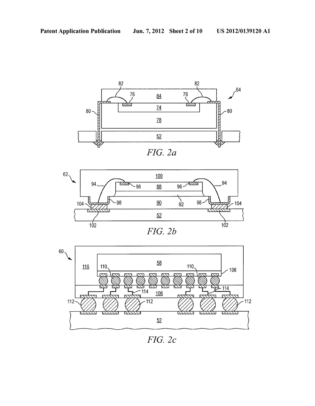
Semiconductor Device and Method of Forming Openings Through Encapsulant to Reduce Warpage and Stress on Semiconductor Package - diagram, schematic, and image 03
Back to Semiconductor Device and Method of Forming Openings Through Encapsulant to Reduce Warpage and Stress on Semiconductor Package , All Patents .