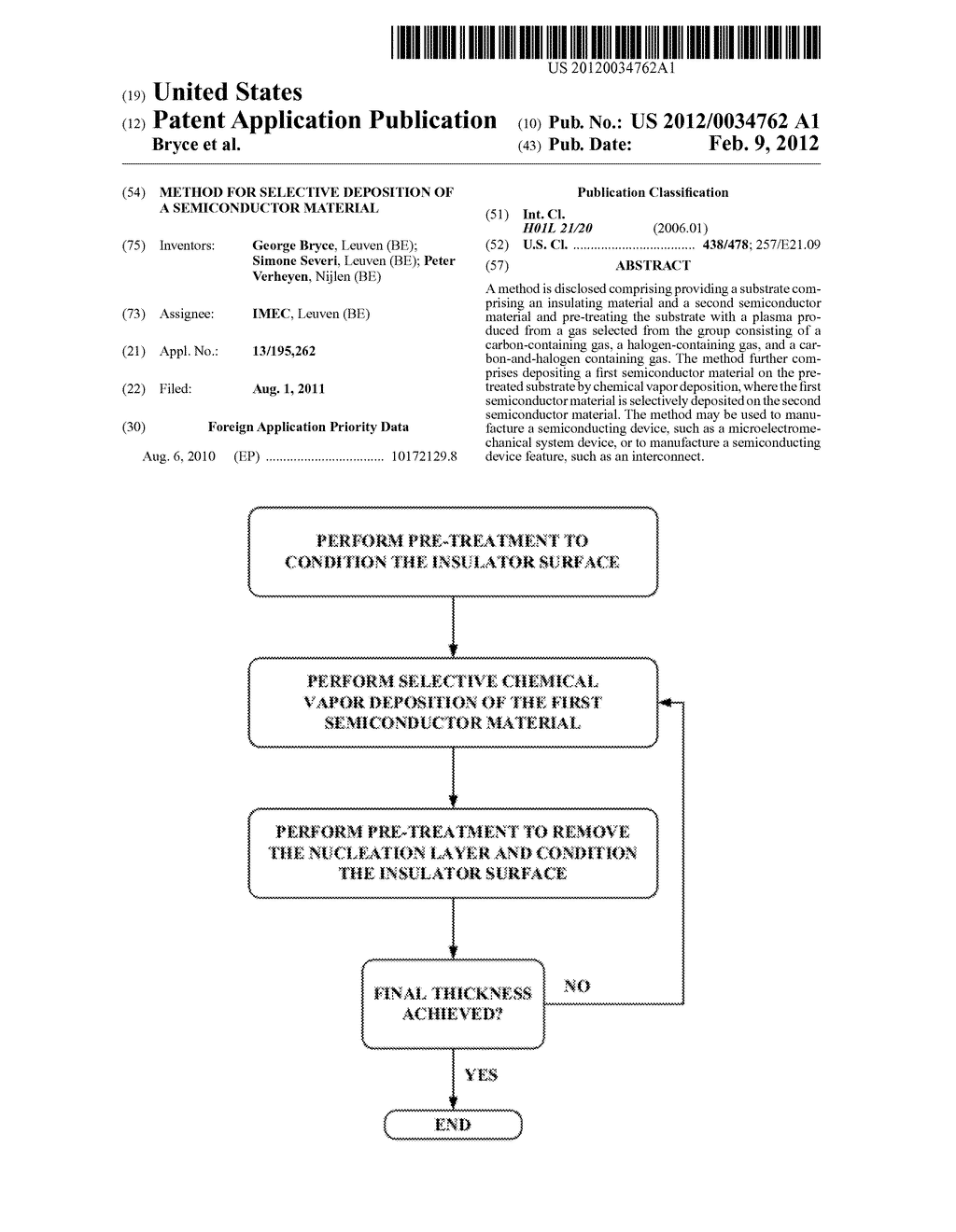
Method for Selective Deposition of a Semiconductor Material - diagram, schematic, and image 01
Back to Method for Selective Deposition of a Semiconductor Material , All Patents .
Back to Method for Selective Deposition of a Semiconductor Material , All Patents .