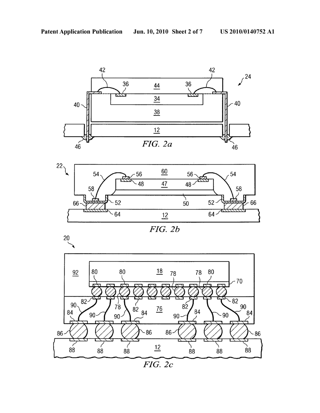
Semiconductor Device and Method of Forming Compliant Polymer Layer Between UBM and Conformal Dielectric Layer/RDL for Stress Relief - diagram, schematic, and image 03
Back to Semiconductor Device and Method of Forming Compliant Polymer Layer Between UBM and Conformal Dielectric Layer/RDL for Stress Relief , All Patents .