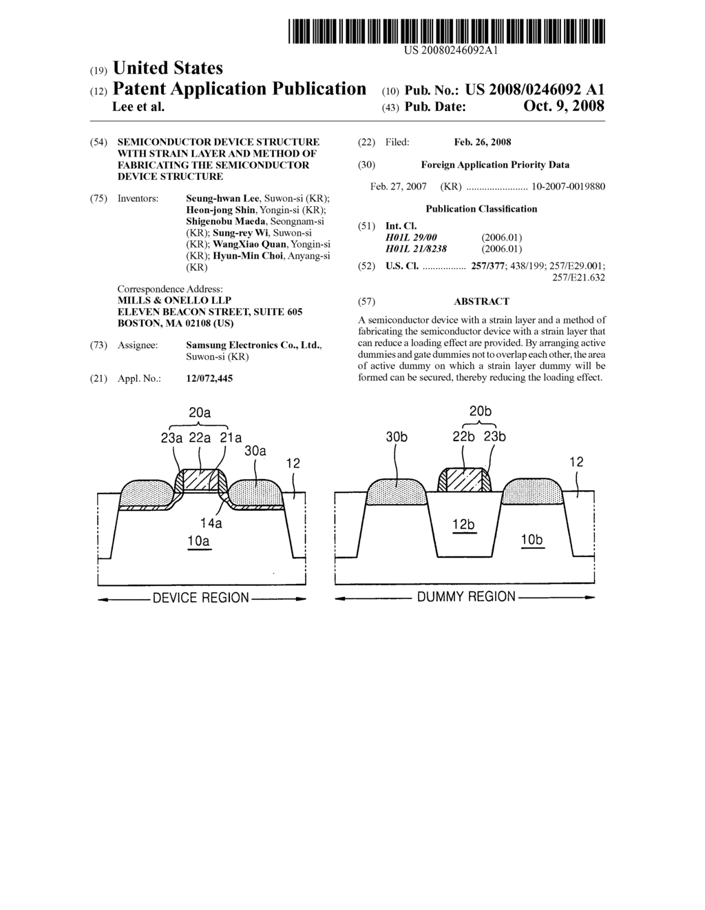
Semiconductor device structure with strain layer and method of fabricating the semiconductor device structure - diagram, schematic, and image 01
Back to Semiconductor device structure with strain layer and method of fabricating the semiconductor device structure , All Patents .