Patent application title: DRIVING VOLTAGE GENERATOR AND DIGITAL TO ANALOG CONVERTER
Inventors:
Jhih-Siou Cheng (New Taipei City, TW)
Ju-Lin Huang (Hsinchu County, TW)
Ju-Lin Huang (Hsinchu County, TW)
Pang-Chan Hung (Kaohsiung City, TW)
IPC8 Class: AH03M176FI
USPC Class:
345690
Class name: Computer graphics processing and selective visual display systems display driving control circuitry intensity or color driving control (e.g., gray scale)
Publication date: 2015-12-31
Patent application number: 20150381197
Abstract:
A digital to analog converter is disclosed. The invention provides a
digital to analog converter (DAC) including a plurality of voltage
transmitting switches and a selecting signal decoder. The voltage
transmitting switches respectively receive a plurality of input voltages,
and output terminals of the voltage transmitting switches are commonly
coupled to an output terminal of the digital to analog converter. The
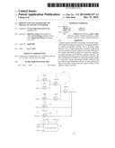
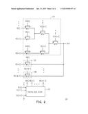
selecting signal decoder receives a plurality of selecting signals, and
generates a plurality of transmitting enable signals to control the
voltage transmitting switches. Wherein only one of the voltage
transmitting switches is connected between each of the input voltages and
the output terminal of the digital to analog converter.Claims:
1. A digital to analog converter, comprising: a plurality of voltage
transmitting switches, respectively receiving a plurality of input
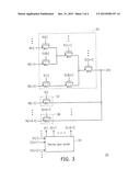
voltages, and output terminals of the voltage transmitting switches being
commonly coupled to an output terminal of the digital to analog
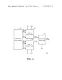
converter; and a selecting signal decoder, receiving a plurality of
selecting signals, and generating a plurality of transmitting enable
signals to control the voltage transmitting switches, wherein only one of
the voltage transmitting switches is connected between each of the input
voltages and the output terminal of the digital to analog converter.
2. The digital to analog converter as claimed in claim 1, wherein at most one of the voltage transmitting switches is turned on according to the transmitting enable signals.
3. The digital to analog converter as claimed in claim 1, wherein the voltage transmitting switches are respectively formed by a plurality of transistors.
4. The digital to analog converter as claimed in claim 3, wherein types of the transistors are the same.
5. A driving voltage generator, adapted to a display device, and comprising: a first digital to analog converter, comprising: a plurality of first voltage transmitting switches, respectively receiving a plurality of first input voltages, and output terminals of the first voltage transmitting switches being commonly coupled to an output terminal of the first digital to analog converter; and a first selecting signal decoder, receiving a plurality of first selecting signals, and generating a plurality of first transmitting enable signals to control the first voltage transmitting switches, wherein only one of the first voltage transmitting switches is connected between each of the first input voltages and the output terminal of the first digital to analog converter.
6. The driving voltage generator as claimed in claim 5, further comprising: a second digital to analog converter, comprising: a plurality of second voltage transmitting switches, respectively receiving a plurality of second input voltages, and output terminals of the second voltage transmitting switches being commonly coupled to an output terminal of the second digital to analog converter; and a second selecting signal decoder, receiving a plurality of second selecting signals, and generating a plurality of second transmitting enable signals to control the second voltage transmitting switches, wherein only one of the second voltage transmitting switches is connected between each of the second input voltages and the output terminal of the second digital to analog converter.
7. The driving voltage generator as claimed in claim 6, further comprising: a gamma input voltage generator, coupled to the first digital to analog converter and the second digital to analog converter, and generating the first and the second gamma input voltages.
8. The driving voltage generator as claimed in claim 6, further comprising: a driving voltage output buffer, coupled to the first and the second output terminals, and selecting a voltage on the first output terminal or the second output terminal according to a polarity selecting signal to generate a driving output voltage.
9. The driving voltage generator as claimed in claim 6, wherein at most one of the first voltage transmitting switches is turned on according to the first transmitting enable signals, and at most one of the second voltage transmitting switches is turned on according to the second transmitting enable signals.
10. The driving voltage generator as claimed in claim 6, wherein the first and second voltage transmitting switches are respectively formed by a plurality of transistors.
11. The driving voltage generator as claimed in claim 10, wherein types of the transistors are the same.
Description:
CROSS-REFERENCE TO RELATED APPLICATION
[0001] This is a continuation application of and claims the priority benefit of U.S. application Ser. No. 13/740,282, filed on Jan. 14, 2013, now allowed. The prior U.S. application Ser. No. 13/740,282 claims the priority benefit of Taiwan application serial no. 101124260, filed on Jul. 5, 2012. The entirety of each of the above-mentioned patent applications is hereby incorporated by reference herein and made a part of this specification.
BACKGROUND
[0002] 1. Technical Field
[0003] The invention relates to a driving voltage generator and a digital-to-analog converter thereof.
[0004] 2. Related Art
[0005] In a display device, in order to present images with correct gray levels on a display panel, a source driver of the display device is required to provide a correct gamma voltage to the display panel according to gray level data to be displayed on the display panel. Therefore, a digital to analog converter (DAC) is used on the source driver of the display device to produce an analog driving output voltage according to digital gray level data, and the display panel is driven to display images according to the driving output voltage.
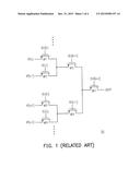
[0006] Referring to FIG. 1, FIG. 1 is a circuit diagram of a DAC 100 of the conventional technique. The DAC 100 includes switches formed by a plurality of transistors MP1-MP11. The switches formed by the transistors MP1-MP7 are grouped into three stages, and the transistors MP1-MP4 arranged in a first stage respectively receive four gamma input voltages VP[n]-VP[n+3], and the transistors MP1, MP3 and the transistors MP2, MP4 are respectively controlled by selecting signals SEL[n] and SELB[n], wherein the selecting signal SELB[n] is an inverted signal of the selecting signal SEL[n]. Moreover, the transistors MP5 and MP6 arranged in a second stage respectively receive a voltage on a common coupling node of the transistors MP1 and MP2 and a voltage on a common coupling node of the transistors MP3 and MP4. The transistors MP5 and MP6 are respectively turned on or turned off under control of selecting signals SEL[n+1] and SELB[n+1]. The transistor MP7 is coupled to a common coupling node of the transistors MP5 and MP6, and is turned on or turned off under control of a selecting signal SELB[n+2], and the transistor MP7 is used to determine whether or not to provide the voltage on the common coupling node of the transistors MP5 and MP6 to serve as a driving output voltage VOUTP.
[0007] According to FIG. 1, it is known that when any of the gamma input voltages VP[n]-VP[n+3] is transmitted to serve as the driving output voltage VOUTP, it has to passes through three transistor switches. Namely, in the conventional DAC 100, a transmission path from which the gamma input voltage is transmitted to serve as the driving output voltage VOUTP has a certain transmission resistance. Such transmission resistance increases as the number of the gamma input voltages increases, which may even influence the quality of the driving output voltage VOUTP. Moreover, in the DAC 100 of the conventional technique, the number of the required transistor switches increases as the number of converted bits increases, which greatly increases a required circuit area.
SUMMARY
[0008] The invention is directed to a digital to analog converter (DAC), which effectively reduces a conducting resistance between an input voltage and an output voltage, and reduces a circuit layout area.
[0009] The invention is directed to a driving voltage generator, which effectively reduces a conducting resistance between an input voltage and an output voltage of a DAC, and reduces a circuit layout area.
[0010] The invention provides a digital to analog converter (DAC) including a plurality of voltage transmitting switches and a selecting signal decoder. The voltage transmitting switches respectively receive a plurality of input voltages, and output terminals of the voltage transmitting switches are commonly coupled to an output terminal of the digital to analog converter. The selecting signal decoder receives a plurality of selecting signals, and generates a plurality of transmitting enable signals to control the voltage transmitting switches. Wherein only one of the voltage transmitting switches is connected between each of the input voltages and the output terminal of the digital to analog converter.
[0011] The invention provides a driving voltage generator, which is adapted to a display device. The driving voltage generator includes a first digital to analog converter (DAC), and the first DAC includes a plurality of first voltage transmitting switches and a first selecting signal decoder. The first voltage transmitting switches respectively receive a plurality of first input voltages, and output terminals of the first voltage transmitting switches are commonly coupled to an output terminal of the digital to analog converter. The first selecting signal decoder receives a plurality of first selecting signals, and generates a plurality of first transmitting enable signals to control the voltage transmitting switches. Wherein only one of the first voltage transmitting switches is connected between each of the input voltages and the output terminal of the first digital to analog converter.
[0012] According to the above descriptions, in the DAC of the invention, one or a plurality of voltage transmitting switches are provided, and the input voltages received by the voltage transmitting switches are directly transmitted to the output terminal of the DAC according to the transmitting enable signals generated by the selecting signal decoder. In this way, the input voltages received by the voltage transmitting switches are unnecessary to be selected and output by a voltage selector having a complicated circuit structure, but can be directly transmitted to the output terminal of the DAC through the voltage transmitting switches at a required time, which may effectively reduce a resistance value of a path used for transmitting the input voltages to the output terminal. Moreover, by transmitting the input voltages through simple voltage transmitting switches, a circuit layout area can be effectively reduced. The invention further provides the driving voltage generator using the aforementioned DAC, and the driving voltage generator is adapted to a display device, and is used for providing a more accurate gamma input voltage to serve as the driving output voltage, so as to improve display performance.
[0013] In order to make the aforementioned and other features and advantages of the invention comprehensible, several exemplary embodiments accompanied with figures are described in detail below.
BRIEF DESCRIPTION OF THE DRAWINGS
[0014] The accompanying drawings are included to provide a further understanding of the invention, and are incorporated in and constitute a part of this specification. The drawings illustrate embodiments of the invention and, together with the description, serve to explain the principles of the invention.
[0015] FIG. 1 is a circuit diagram of a digital to analog converter (DAC) 100 of a conventional technique.
[0016] FIG. 2 is a schematic diagram of a DAC 200 according to an embodiment of the invention.
[0017] FIG. 3 is a schematic diagram of a DAC 300 according to another embodiment of the invention.
[0018] FIG. 4 is a driving voltage generator 400 according to an embodiment of the invention.
DETAILED DESCRIPTION OF DISCLOSED EMBODIMENTS
[0019] Referring to FIG. 2, FIG. 2 is a schematic diagram of a digital to analog converter (DAC) 200 according to an embodiment of the invention. The DAC 200 includes a voltage selector 210, voltage transmitting switches 221-22M and a selecting signal decoder 230. The voltage selector 210 receives voltages VP[n]-VP[n+2] among a plurality of input voltages VP[n]-VP[n+M-4] of an analog format, and receives a plurality of selecting signals SEL[n]-SEL[n+2] and selecting signals SELB[n]-SELB[n+2] of a digital format, where the selecting signals SELB[n]-SELB[n+2] are respectively inverted signals of the selecting signals SEL[n]-SEL[n+2]. The voltage selector 210 selects at most one of the voltages VP[n]-VP[n+2] for providing to an output terminal OUT1 according to the selecting signals SEL[n]-SEL[n+2] and SELB[n]-SELB[n+2].
[0020] In the present embodiment, the voltage selector 210 includes a plurality of switches formed by transistors MP21-MP26. The transistors MP21 and MP22 are used to select one of the input voltages VP[n] and VP[n+1] for transmitting to one terminal of the transistor MP24. The transistor MP21 is turned on or turned off under control of the selecting signal SELB[n], and the transistor MP22 is turned on or turned off under control of the selecting signal SEL[n]. Moreover, the transistor MP23 receives the input voltage VP[n+2], and is controlled by the selecting signal SELB[n]. Namely, when the transistors MP21 and MP22 transmit the input voltage VP[n] to the transistor MP24 according to the selecting signals SEL[n] and SELB[n] (the input voltage VP[n] is equal to a voltage V1), the transistor MP23 is simultaneously turned on, and transmits the input voltage VP[n+2] to one terminal of the transistor MP25 (the input voltage VP[n+2] is equal to a voltage V2). Comparatively, when the transistors MP21 and MP22 transmit the input voltage VP[n+1] to the transistor MP24 according to the selecting signals SEL[n] and SELB[n] (the input voltage VP[n+1] is equal to the voltage V1), the transistor MP23 is turned off, and a coupling node between the transistor MP23 and the transistor MP25 is in a floating state (the voltage V2 has a high impedance).
[0021] The transistors MP24 and MP25 are used to select one of the voltages V1 and V2 for outputting to the transistor MP26 under control of the selecting signals SELB[n+1] and SEL[n+1]. The transistor M26 is turned on or turned off under control of the selecting signal SELB[n+2], and determines whether or not to output one of the voltages V1 and V2 to the output terminal OUT1 to serve as an output voltage.
[0022] Moreover, in the present embodiment, the voltage transmitting switches 221-22M are respectively implemented by transistors MP27-MP28. The transistors MP27-MP28 are respectively turned on or turned off under control of transmitting enable signals HB[n]-HB[n+M-4]. It should be noticed that at most one of the transistors MP27-MP28 is turned on for directly transmitting one of the received input voltages VP [n+3]-VP[n+M-4] to the output terminal OUT1. Moreover, the transistor MP26 in the voltage selector 210 is now in a turn-off state. The aforementioned n and M are all positive integers.
[0023] Certainly, the transistors MP27-MP28 can be all turned off, and the voltage transmitting switches 221-22M do not transmit any voltage to the output terminal OUT1, and in this case, the transistor MP26 in the voltage selector 210 must be in a turn-on state and transmits a voltage on a coupling node of the transistors MP24 and MP25 to the output terminal OUT1.
[0024] It should be noticed that the input voltages VP[n+3]-VP[n+M-4] can be transmitted to the output terminal OUT1 through one of the voltage transmitting switches 221-22M constructed by the single transistor MP27 or MP28. Namely, when the DAC 200 transmits one of the input voltages VP[n+3]-VP[n+M-4] to serve as the output voltage, a transmission impedance is very small. Under a high speed operation of the DAC 200, a delay time required for effectively transmitting the input voltages VP[n+3]-VP[n+M-4] with relatively great voltage absolute values to the output terminal OUT1 can be effectively shortened. Namely, the output voltage generated by the DAC 200 can be more accurate.
[0025] The selecting signal decoder 230 is coupled to the voltage transmitting switches 221-22M, and receives the selecting signals SEL[n]-SEL[n+2]. The selecting signal decoder 230 generates the transmitting enable signals HB[n]-HB[n+M-4] according to the selecting signals SEL[n]-SEL[n+2] and/or inverted signals SELB[n]-SELB[n+2] thereof. The selecting signal decoder 230 can be implemented by a logic operation circuit. For example, in case that the transistors MP21-MP28 are all P-type transistors, when the DAC 200 transmits one of the input voltages VP [n+3]-VP [n+M-4] to the output terminal OUT1 according to the selecting signals SEL[n]-SEL[n+2], the selecting signal decoder 230 makes one of the transmitting enable signals HB[n]-HB[n+M-4] to a logic low level, and makes other transmitting enable signals to a logic high level.
[0026] Referring to FIG. 3, FIG. 3 is a schematic diagram of a DAC 300 according to another embodiment of the invention. The DAC 300 includes a voltage selector 310, voltage transmitting switches 321-32M and a selecting signal decoder 330. The voltage selector 310 receives voltages VN[n]-VN[n+2] among a plurality of input voltages VN[n]-VN[n+M-4] of the analog format, and receives a plurality of selecting signals SEL[n]-SEL[n+2] and selecting signals SELB[n]-SELB[n+2] of the digital format, where the selecting signals SELB[n]-SELB[n+2] are respectively inverted signals of the selecting signals SEL[n]-SEL[n+2]. The voltage selector 310 selects at most one of the voltages VP[n]-VP[n+2] for providing to an output terminal OUT2 according to the selecting signals SEL[n]-SEL[n+2] and SELB[n]-SELB[n+2]. Terminals of the voltage transmitting switches 321-32M respectively receive voltages VN[n+3]-VN[n+M-4] among the input voltages VN[n]-VN[n+M-4]. Other terminals of the voltage transmitting switches 321-32M are commonly coupled to the output terminal OUT2. The voltage transmitting switches 321-32M are respectively turned on or turned off according to transmitting enable signals H[n]-H[n+M-4].
[0027] Different to the embodiment of FIG. 2, the switches of the present embodiment are all implemented by N-type transistors, so that signals used for controlling transistors MN21-MN28 are all inverted to signals used for controlling the transistors MP21-MP28 of FIG. 2. Operation details of the present embodiment are similar to that of the embodiment of FIG. 2, which are not repeated.
[0028] Referring to FIG. 4, FIG. 4 is a driving voltage generator 400 according to an embodiment of the invention. The driving voltage generator 400 is adapted to a display device, and the display device is, for example, a liquid crystal display (LCD) or a light-emitting diode (LED) display, etc. In the present embodiment, the display device is, for example, an LCD, and the driving voltage generator 400 includes a gamma input voltage generator 410, DACs 421 and 422, and a driving voltage output buffer 430. The gamma input voltage generator 410 is coupled to the DACs 421 and 422, and is used for generating gamma input voltages VP1-VPP and VN1-VNP. The DACs 421 and 422 respectively receive the gamma input voltages VP1-VPP and VN1-VNP and selecting signals SEL and SELB, and respectively generate output voltages VOUT1 and VOUT2 the output terminals thereof for outputting to the driving voltage output buffer 430. The driving voltage output buffer 430 is coupled to the output terminals of the DACs 421 and 422, and selects one of the voltages on the output ten finals of the DACs 421 and 422 according to a polarity selecting signal POL to generate a driving output voltage VDRV.
[0029] It should be noticed that regarding implementation details of the DACs 421 and 422, the DAC 421 can be implemented by the DAC 200 of the embodiment of FIG. 2, and the DAC 422 can be implemented by the DAC 300 of the embodiment of FIG. 3, where the DAC 421 is used to select the positive gamma input voltages VP1-VPP to generate the output voltage VOUT1, and the DAC 422 is used to select the negative gamma input voltages VN1-VNP to generate the output voltage VOUT2.
[0030] Moreover, the selecting signals SEL and SELB can be generated according to gray level data of a frame to be displayed by the display device. Generally, each of the selecting signals SEL and SELB makes the DACs 421 and 422 to respectively generate the output voltages VOUT1 and VOUT2, where the selecting signal SEL is inverted to the selecting signal SELB.
[0031] Here, the DACs 421 and 422 are not all necessary, and if the DACs are applied to the LED display that the driving voltage generator 400 does not have driving polarity, one of the DACs 421 and 422 can be used according to positive and negative of the driving output voltage. Certainly, in this case, the driving voltage output buffer 430 is unnecessary to receive the polarity selecting signal POL, and only driving capability of the output voltage VOUT1 or VOUT2 is required to be strengthened to generate the driving output voltage VDRV.
[0032] In summary, in the DAC of the invention, besides the voltage selector, voltage transmitting switches are further configured, and it is set that a part of the voltages in the input voltages are transmitted to the output terminal of the DAC through the voltage transmitting switches. In this way, when the input voltages coupled to the voltage transmitting switches are transmitted, the input voltages are unnecessary to pass through a voltage transmission path with a high impedance, so that the input voltages can be quickly transmitted to the output terminal, which enhances a voltage conversion efficiency of the DAC. Moreover, by configuring the simple voltage transmitting switches, a circuit area can be effectively decreased to save a cost. It should be noticed that the DAC of the invention can be applied to a driving voltage generator of a display device, and in case that a displayed frame has a high frame refreshing rate, display performance can be effectively improved and the number of circuit components are decreased, and both of product quality and price competitiveness are enhanced.
[0033] It will be apparent to those skilled in the art that various modifications and variations can be made to the structure of the invention without departing from the scope or spirit of the invention. In view of the foregoing, it is intended that the invention cover modifications and variations of this invention provided they fall within the scope of the following claims and their equivalents.
User Contributions:
Comment about this patent or add new information about this topic:
Images included with this patent application:
 |  |
 |  |
 |
| Similar patent applications: | |
| Date | Title |
|---|---|
| 2016-03-03 | Extension of the mpeg/sc3dmc standard to polygon meshes |
| 2016-04-21 | Novel driving algorithm on projected capacitance touch |
| 2015-10-15 | Graphical indicators in analog clock format |
| 2016-04-07 | 3-dimensional model generation using edges |
| 2016-04-14 | Method and apparatus for modeling target object to represent smooth silhouette |
| New patent applications in this class: | |
| Date | Title |
|---|---|
| 2022-05-05 | Pixel circuit and driving method thereof, array substrate and diisplay apparatus |
| 2022-05-05 | Display device and driving method of the same |
| 2022-05-05 | Display device |
| 2022-05-05 | Display device performing peak luminance driving, and method of operating a display device |
| 2022-05-05 | Display driver and display device |
| New patent applications from these inventors: | |
| Date | Title |
|---|---|
| 2021-12-16 | Source driver and driving circuit thereof |
| 2021-12-09 | Light-emitting diode driving apparatus and light-emitting diode driver |
| 2021-12-02 | Method of controlling display panel and control circuit using the same |
| 2021-11-11 | Source driver and calibration method thereof |
| Top Inventors for class "Computer graphics processing and selective visual display systems" | |
| Rank | Inventor's name |
|---|---|
| 1 | Katsuhide Uchino |
| 2 | Junichi Yamashita |
| 3 | Tetsuro Yamamoto |
| 4 | Shunpei Yamazaki |
| 5 | Hajime Kimura |