Patent application title: COATED ARTICLE AND METHOD FOR MANUFACTURING SAME
Inventors:
Hsin-Pei Chang (Tu-Cheng, TW)
Hsin-Pei Chang (Tu-Cheng, TW)
Wen-Rong Chen (Tu-Cheng, TW)
Wen-Rong Chen (Tu-Cheng, TW)
Huann-Wu Chiang (Tu-Cheng, TW)
Huann-Wu Chiang (Tu-Cheng, TW)
Cheng-Shi Chen (Tu-Cheng, TW)
Xiao-Qiang Chen (Shenzhen, CN)
Assignees:
HON HAI PRECISION INDUSTRY CO., LTD.
HONG FU JIN PRECISION INDUSTRY (ShenZhen) CO., LTD.
IPC8 Class: AB32B1520FI
USPC Class:
428215
Class name: Including components having same physical characteristic in differing degree thickness (relative or absolute) absolute thicknesses specified
Publication date: 2012-02-09
Patent application number: 20120034438
Abstract:
A coated article comprises a substrate; a bonding layer deposited on the
substrate; and a composite layer deposited on the bonding layer. The
composite layer includes an equal number of alternating chromium-nitride
layers and aluminum-nitride layers.Claims:
1. A coated article, comprising: a substrate; a bonding layer deposited
on the substrate; and a composite layer deposited on the bonding layer,
the composite layer comprising an equal number of alternating
chromium-nitride layers and aluminum-nitride layers.
2. The coated article as claimed in claim 1, wherein the substrate is made of stainless steel, aluminum, aluminum alloy, ceramic or glass.
3. The coated article as claimed in claim 1, wherein the bonding layer is an aluminum layer.
4. The coated article as claimed in claim 3, wherein the bonding layer has a thickness between 50 nanometers and 300 nanometers.
5. The coated article as claimed in claim 1, wherein the number of the chromium-nitride layers and the number of the aluminum-nitride layers are both between 6 and 10.
6. The coated article as claimed in claim 1, wherein each chromium-nitride layer has a thickness between about 40 nanometers and about 150 nanometers.
7. The coated article as claimed in claim 1, wherein each aluminum-nitride layer has a thickness between about 40 nanometers and about 150 nanometers.
8. The coated article as claimed in claim 1, wherein the composite layer bonds with the substrate by a chromium-nitride layer or an aluminum-nitride layer.
9. A method for manufacturing a coated article, the method comprising: providing a substrate made of made of stainless steel, aluminum, aluminum alloy, ceramic or glass; depositing a bonding layer on the substrate; and depositing a composite layer on the bonding layer, wherein the composite layer comprises an equal number of alternating chromium-nitride layers and aluminum-nitride layers.
10. The method of claim 9, wherein during depositing the bonding layer on the substrate, the substrate is retained in a vacuum chamber; pure argon is floated into the vacuum chamber at a flux between about 50 sccm and 300 sccm; an aluminum target in the vacuum chamber is evaporated; a bias voltage applied to the substrate is between about -150 volts and -500 volts to deposit the bonding layer on the substrate.
11. The method of claim 10, wherein the bonding layer has a thickness between 50 nanometers and 300 nanometers
12. The method of claim 10, wherein during depositing the composite layer on the bonding layer, pure argon is floated into the vacuum chamber at a flux between about 300 sccm and about 500 sccm; nitrogen is floated into the vacuum chamber at a flux between about 10 sccm and about 150 sccm; a bias voltage applied to the substrate is between about -150 volts and -500 volts; the aluminum target and a chromium target in the vacuum chamber are alternatively evaporated to deposit an equal number of alternating chromium-nitride layers and aluminum-nitride layers on the substrate.
13. The method of claim 12, wherein the number of the chromium-nitride layers and the number of the aluminum-nitride layers are equal and between 6 and 10 of each layer.
14. The method of claim 9, wherein each chromium-nitride layer has a thickness between about 40 nanometers and about 150 nanometers.
15. The method of claim 9, wherein each aluminum-nitride layer has a thickness between about 40 nanometers and about 150 nanometers.
Description:
BACKGROUND
[0001] 1. Technical Field
[0002] The disclosure generally relates to coated articles and method for manufacturing the coated articles.
[0003] 2. Description of Related Art
[0004] Aluminum alloy has good heat dissipation properties and can also effectively shield electromagnetic interference. Therefore, aluminum alloy is widely used to manufacture housings of electronic devices. However, aluminum alloy has low corrosion resistance. For improving the corrosion resistance of the aluminum alloy, physical vapor deposition (PVD) has been used to form a coating on the alloy. However, aluminum alloy typically has a plurality of micropores causing the coating on the aluminum alloy correspondingly having a plurality of micropores exposing the alloy to pollutants that penetrate through the micropores.
[0005] Therefore, there is room for improvement within the art.
BRIEF DESCRIPTION OF THE DRAWINGS
[0006] Many aspects of the embodiments can be better understood with reference to the following drawings. The components in the drawings are not necessarily drawn to scale, the emphasis instead being placed upon clearly illustrating the principles of the exemplary coated article and method for manufacturing the coated article. Moreover, in the drawings like reference numerals designate corresponding parts throughout the several views. Wherever possible, the same reference numbers are used throughout the drawings to refer to the same or like elements of an embodiment.
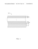
[0007] FIG. 1 illustrates a cross-sectional view of an exemplary embodiment of a coated article.
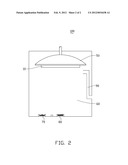
[0008] FIG. 2 is a schematic view of a magnetron sputtering coating machine for manufacturing the coated article in FIG. 1.
DETAILED DESCRIPTION
[0009] Referring to FIG. 1, a coated article 100 includes a substrate 10, a bonding layer 20 and a composite layer 30 deposited on the bonding layer 20. The substrate 10 may be made of stainless steel, aluminum, aluminum alloy, ceramic, or glass. The bonding layer 20 is an aluminum layer and has a thickness between 50 nanometers and 300 nanometers. The bonding layer 20 may be deposited on the substrate 10 by magnetron sputtering. The composite layer 30 includes an equal number of alternating chromium-nitride layers 301 and aluminum-nitride layers 303. The equal number of chromium-nitride layers 301 and aluminum-nitride layers 303 may be between 6 and 10 of each. Each chromium-nitride layer 301 has a thickness between about 40 nanometers and about 150 nanometers. Each aluminum-nitride layer 303 has a thickness between about 40 nanometers and about 150 nanometers. The chromium-nitride layers 301 and the aluminum-nitride layers 303 may be deposited by magnetron sputtering. The composite layer 30 bonds/contacts with the substrate 10 by a chromium-nitride layer 301 or an aluminum-nitride layer 303.
[0010] Referring to FIG. 2, a method for manufacturing the coated article 100 may include at least the following steps.
[0011] Providing a substrate 10. The substrate 10 may be made of stainless steel, aluminum, aluminum alloy, ceramic or glass.
[0012] Pre-treating the substrate 10, by washing it with a solution (e.g., alcohol or acetone), which can be done in an ultrasonic cleaner, to remove impurities, such as grease, or dirt. The substrate 10 is dried. The substrate 10 is then cleaned by argon plasma cleaning. The substrate 10 is retained on a rotating bracket 50 in a vacuum chamber 60 of a magnetron sputtering coating machine 100 with vacuum level at 8.0×10⁻³ Pa. Pure argon is fed into the vacuum chamber 60 at a flux between about 50 Standard Cubic Centimeters per Minute (sccm) and 400 sccm from a gas inlet 90. A bias voltage applied to the substrate 10 is between -300 V to -600 V for about 5-10 minutes. Thus, the substrate 10 is washed by argon plasma, to further remove grease or dirt. As a result, the binding force between the substrate 10 and the composite layer 30 is enhanced.
[0013] Depositing a bonding layer 20 on the substrate 10, pure argon is floated into the vacuum chamber 60 at a flux between about 50 sccm and 300 sccm from the gas inlet 90. An aluminum target 70 in the vacuum chamber 60 is evaporated. A bias voltage applied to the substrate 10 is between about -150 volts and -500 volts to deposit the bonding layer 20 on the substrate 10. The bonding layer 20 has a thickness between 50 nanometers and 300 nanometers
[0014] A composite layer 30 is deposited on the bonding layer 20. Pure argon is pumped into the vacuum chamber 60 at a flux between about 300 sccm and about 500 sccm from the gas inlets 24. Nitrogen is pumped into the vacuum chamber 60 at a flux between about 10 sccm and about 150 sccm from the gas inlets 24. A bias voltage applied to the substrate 10 is between about -150 volts and -500 volts. The aluminum target 70 and a chromium target 80 in the vacuum chamber 60 are alternatively evaporated to deposit an equal number of alternating chromium-nitride layers 301 and aluminum-nitride layers 303 on the substrate 10. The equal number of chromium-nitride layers 301 and aluminum-nitride layers 303 may be between 6 and 10 of each. Each chromium-nitride layer 301 has a thickness between about 40 nanometers and about 150 nanometers. Each aluminum-nitride layer 303 has a thickness between about 40 nanometers and about 150 nanometers.
[0015] The alternating chromium-nitride layers 301 and aluminum-nitride layers 303 have a good compactness that can improve the corrosion resistance of the composite layer 30, to prevent the coated article 100 from being corroded by pollutants. Additionally, the bonding layer 20 not only can enhance the binding force between the substrate 10 and the composite layer 30, but also can decrease the electrical potential difference between the composite layer 30 and the substrate 10, to further improve the corrosion resistance of the composite layer 30.
[0016] It is to be understood, however, that even through numerous characteristics and advantages of the exemplary disclosure have been set forth in the foregoing description, together with details of the system and function of the disclosure, the disclosure is illustrative only, and changes may be made in detail, especially in matters of shape, size, and arrangement of parts within the principles of the disclosure to the full extent indicated by the broad general meaning of the terms in which the appended claims are expressed.
User Contributions:
Comment about this patent or add new information about this topic:
Images included with this patent application:
 |  |
 |
| New patent applications in this class: | |
| Date | Title |
|---|---|
| 2019-05-16 | Multi-layer film with improved modulus properties |
| 2018-01-25 | Vehicle headliner material |
| 2017-08-17 | Composite material |
| 2016-12-29 | Flexible metal laminate and preparation method of the same |
| 2016-09-01 | Thin laminate structures with enhanced acoustic performance |
| New patent applications from these inventors: | |
| Date | Title |
|---|---|
| 2013-07-04 | Anti-counterfeiting article and method thereof |
| 2013-07-04 | Tag holder and workpiece using the same |
| 2013-06-20 | Composite and method for making the same |
| 2013-05-30 | Anti-theft system using rfid tags |
| Top Inventors for class "Stock material or miscellaneous articles" | |
| Rank | Inventor's name |
|---|---|
| 1 | Cheng-Shi Chen |
| 2 | Hsin-Pei Chang |
| 3 | Wen-Rong Chen |
| 4 | Huann-Wu Chiang |
| 5 | Shou-Shan Fan |