Patent application title: Method for Fabricating Selectively Coupled Optical Waveguides on a Substrate
Inventors:
Craig M. Hill (Warrenton, VA, US)
Mark Jaso (Fairfax Station, VA, US)
IPC8 Class: AG02B612FI
USPC Class:
385 14
Class name: Optical waveguides integrated optical circuit
Publication date: 2010-01-21
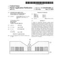
Patent application number: 20100014804
Inventors list |
Agents list |
Assignees list |
List by place |
Classification tree browser |
Top 100 Inventors |
Top 100 Agents |
Top 100 Assignees |
Usenet FAQ Index |
Documents |
Other FAQs |
Patent application title: Method for Fabricating Selectively Coupled Optical Waveguides on a Substrate
Inventors:
Craig M Hill
Mark Jaso
Agents:
BAE SYSTEMS
Assignees:
Origin: NASHUA, NH US
IPC8 Class: AG02B612FI
USPC Class:
385 14
Patent application number: 20100014804
Abstract:
A method for fabricating selectively coupled optical waveguides on a
substrate is disclosed. Initially, a first layer of waveguide material is
deposited on a substrate. The first layer of waveguide material is then
etched to form multiple level one waveguides and fill shapes. A
dielectric layer is deposited on top of the level one waveguides and fill
shapes. The surface profile of the dielectric layer deposition tracks the
pattern density of the fill shapes. After the surface of the dielectric
layer has been polished, a second layer of waveguide material is
deposited on the substrate. At least one optically coupled waveguide
structure, which is formed by a first level one waveguide and a first
level two waveguide, is located adjacent to at least one non-optically
coupled waveguide structure, which is formed by a second level one
waveguide and a second level two waveguide.Claims:
1. A method for fabricating selectively coupled optical waveguides on a
substrate, said method comprising:depositing a first layer of waveguide
material on a substrate;etching said first layer of waveguide material to
form a plurality of level one waveguides and fill shapes;depositing a
dielectric layer on top of said level one waveguides and fill shapes,
wherein the deposition surface profile of said dielectric layer tracks
the pattern density of said fill shapes;polishing the surface of said
dielectric layer;depositing a second layer of waveguide material on said
substrate; andetching said second layer of waveguide material to form a
plurality of level two waveguides, wherein at least one optically coupled
waveguide structure is formed by a first one of said level one waveguides
and a first one of said level two waveguides, and at least one
non-optically coupled waveguide structure is formed by a second one of
said level one waveguides and a second one of said level two waveguides,
wherein said at least one optically coupled waveguide structure is
located adjacent to said at least one non-optically coupled waveguide
structure.
2. The method of claim 1, wherein said optically coupled waveguide structure is optically isolated from said non-optically coupled waveguide structure.
3. The method of claim 1, wherein said depositing further includesetching said dielectric layer utilizing a photo resist layer; andstripping said photo resist layer to leave a via in said dielectric layer for waveguide deposition.
4. A semiconductor structure comprising:a substrate;a plurality of fill shapes;a plurality of level one waveguides separated by said plurality of fill shapes, wherein said plurality of fill shapes and level one waveguides are situated within a dielectric layer located on said substrate; anda plurality of level two waveguides, wherein at least one optically coupled waveguide structure is formed by a first one of said level one waveguides and a first one of said level two waveguides, and at least one non-optically coupled waveguide structure is formed by a second one of said level one waveguides and a second one of said level two waveguides, wherein said at least one optically coupled waveguide structure is located adjacent to said at least one non-optically coupled waveguide structure.
5. The semiconductor structure of claim 4, wherein said optically coupled waveguide structure is optically isolated from said non-optically coupled waveguide structure.
6. The semiconductor structure of claim 4, wherein said plurality of fill shapes have different sizes.
Description:
PRIORITY CLAIM
[0001]The present application claims benefit of priority under 35 U.S.C. § 365 to the previously filed international patent application number PCT/US08/074786 filed on Aug. 29, 2008, assigned to the assignee of the present application, and having a priority date of Oct. 17, 2007, based upon U.S. provisional patent application No. 60/999,235, the contents of both applications are incorporated herein by reference.
BACKGROUND OF THE INVENTION
[0002]1. Technical Field
[0003]The present invention relates to optical waveguides in general, and in particular to a method for fabricating selectively coupled optical waveguides on a substrate.
[0004]2. Description of Related Art
[0005]Although optical waveguides can be fabricated in different layers of a substrate in a stack structure, the difficulties in enabling all those optical waveguides to couple with one another can limit the usefulness of the stacked structure. In order for optical waveguides located in different layers to couple with each other, the vertical distance between them must be a fraction of the optical wavelength, and this distance is much smaller than the typical dielectric thickness required to isolate two layers.
[0006]The entire length of conventionally coupled waveguides are separated by a relatively thin dielectric layer having a uniform thickness. However, the usage of one uniform dielectric thickness across the substrate as the coupling layer does not allow for optically isolating the optical waveguides. Thus, the conventional method of utilizing a thin coupling layer limits the integration density of coupled waveguides due to the relatively large separation distances required to provide optical isolation from adjacent waveguides.
[0007]Consequently, it would be desirable to provide an improved method for fabricating coupled optical waveguides such that optical coupling can be achieved within localized areas while adequate optical isolation from other waveguide structures located in close proximity can also be affained.
SUMMARY OF THE INVENTION
[0008]In accordance with a preferred embodiment of the present invention, a first layer of waveguide material is initially deposited on a substrate. The first layer of waveguide material is then etched to form multiple level one waveguides and fill shapes. A dielectric layer is deposited on top of the level one waveguides and fill shapes. The surface profile of the dielectric layer deposition tracks the pattern density of the fill shapes. After the surface of the dielectric layer has been polished, a second layer of waveguide material is deposited on the substrate. At least one optically coupled waveguide structure, which is formed by a first level one waveguide and a first level two waveguide, is located adjacent to at least one non-optically coupled waveguide structure, which is formed by a second level one waveguide and a second level two waveguide.
[0009]All features and advantages of the present invention will become apparent in the following detailed written description.
BRIEF DESCRIPTION OF THE DRAWINGS
[0010]The invention itself, as well as a preferred mode of use, further objects, and advantages thereof, will best be understood by reference to the following detailed description of an illustrative embodiment when read in conjunction with the accompanying drawings, wherein:
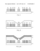
[0011]FIGS. 1-4 are drawings illustrating sequential steps of a method for fabricating selectively coupled optical waveguides, in accordance with a preferred embodiment of the present invention; and
[0012]FIGS. 2a-2b are drawings illustrating the optional steps for decreasing the polishing load in certain area of the dielectric layer in FIG. 2.
DETAILED DESCRIPTION OF A PREFERRED EMBODIMENT
[0013]Referring now to the drawings and in particular to FIGS. 1-4, there are illustrated sequential steps of a method for fabricating selectively coupled optical waveguides, in accordance with a preferred embodiment of the present invention. Initially, a layer of waveguide material is deposited on a substrate 10. The waveguide material layer is then etched using conventional lithographic methods to form level one waveguides 11a-11c and fill shapes 12a-12f, as shown in FIG. 1. Since waveguides 11a-11c and fill shapes 12a-12f are made of the same waveguide material, they are essentially identical from each other (even though they are shown in different colors), except waveguides 11a-11c will actually be utilized to perform the functions of waveguides while fill shapes 12a-12f will only be served as spacers or fillers.
[0014]Next, a dielectric layer 21, such as silicon oxide, silicon dioxide or cladding material, is deposited over substrate 10, covering waveguides 11a-11c and fill shapes 12a-12f, as depicted in FIG. 2. The deposition surface profile of dielectric layer 21 is determined by the pattern density of fill shapes 12a-12f. The pattern density of fill shapes 12a-12f is defined by the individual size of fill shapes 12a-12f, the distances between fill shapes 12a-12f, and the distances between fill shapes 12a-12f and waveguides 11a-11c.
[0015]For example, in FIG. 2, the deposition surface profile of dielectric layer 21 directly above waveguide 11a and fill shapes 12a-12b is relatively flat because of the larger sizes of waveguide 11a and fill shapes 12a-12b as well as the close proximity among waveguide 11a and fill shapes 12a-12b. The deposition surface profile of dielectric layer 21 gradually slopes down from fill shape 12b to waveguide 11b because of the relatively smaller size of fill shape 12c and the relatively longer distance between fill shape 12c and waveguide 11b. Similarly, the deposition surface profile of dielectric layer 21 directly above waveguide 11c and fill shapes 12e-12f is relatively flat because of the larger sizes of waveguide 11c and fill shapes 12e-12f as well as the close proximity among waveguide 11c and fill shapes 12e-12f. The deposition surface profile of dielectric layer 21 gradually slopes down from fill shape 12d to waveguide 11b because of the relatively smaller size of fill shape 12d and the relatively longer distance between fill shape 12d and waveguide 11b.
[0016]A chemical mechanical polishing (CMP) process is subsequently utilized to shave or thin out an area 31 of dielectric layer 21 located directly above waveguide 11b, as shown in FIG. 3. The exact removal amount of dielectric layer 21 is determined by the pattern density of fill shapes 12a-12f and the CMP process.
[0017]A second waveguide material layer is deposited over dielectric layer 21. The second waveguide material layer is then patterned using conventional lithography method to produce level two waveguides 11a-11c, as depicted in FIG. 4. In the present example, area 31 (from FIG. 3) of dielectric layer 21 is thin enough to allow waveguide 41b to be optically coupled to waveguide 11b, but the other areas of dielectric layer 21 are much thicker such that waveguides 41a, 41c are not optically coupled to waveguides 11a, 11c. In addition, adequate optical isolation are maintained between optically coupled waveguides 11b, 41b and other waveguides 11a, 11c, 41a and 41c located in close proximity to optically coupled waveguides 11b, 41b.
[0018]With reference now to FIGS. 2a-2b, there are illustrated the optional steps for decreasing the polishing load at the area of dielectric layer 21 located directly over waveguide 11b in FIG. 2. First, dielectric layer 21 is etched using a photo resist layer 51 placed on dielectric layer 21, as shown in FIG. 2A. Photo resist layer 51 is then stripped leaving a via 61 in dielectric layer 21 for waveguide deposition, as depicted in FIG. 2b. The optional steps are to be performed after FIG. 2 and before FIG. 3.
[0019]As has been described, the present invention provides an improved method for fabricating selectively coupled optical waveguides such that optical coupling can be achieved within localized areas while adequate optical isolation from other waveguide structures located in close proximity can also be attained.
[0020]While the invention has been particularly shown and described with reference to a preferred embodiment, it will be understood by those skilled in the art that various changes in form and detail may be made therein without departing from the spirit and scope of the invention.
User Contributions:
comments("1"); ?> comment_form("1"); ?>Inventors list |
Agents list |
Assignees list |
List by place |
Classification tree browser |
Top 100 Inventors |
Top 100 Agents |
Top 100 Assignees |
Usenet FAQ Index |
Documents |
Other FAQs |
User Contributions:
Comment about this patent or add new information about this topic:
| People who visited this patent also read: | |
| Patent application number | Title |
|---|---|
| 20100015580 | DISH CODING SYSTEM |
| 20100015578 | METHODS OF USING A DENTAL COMPOSITION HAVING AN ACIDIC COMPONENT AND A PHOTOBLEACHABLE DYE |
| 20100015577 | ORTHODONTIC INDIRECT BONDING TRAY WITH MOISTURE CONTROL |
| 20100015574 | Aesthetic ceramic veneered restoration |
| 20100015573 | MATERIAL AND BLANK FOR DENTURES |
Images included with this patent application:
 |  |
 |
| New patent applications in this class: | |
| Date | Title |
|---|---|
| 2019-05-16 | Optical circuit board sheet and opto-electric hybrid board sheet including same |
| 2019-05-16 | Semicondcutor packages |
| 2019-05-16 | Optical bench on substrate |
| 2019-05-16 | Optical isolator bridge |
| 2019-05-16 | Optoelectronic component |
| New patent applications from these inventors: | |
| Date | Title |
|---|---|
| 2012-12-20 | Method of integrating slotted waveguide into cmos process |
| 2012-12-20 | Asymmetric slotted waveguide and method for fabricating the same |
| 2012-12-06 | Method for growing germanium epitaxial films |
| 2012-10-04 | Method for manufacturing lateral germanium detectors |
| Top Inventors for class "Optical waveguides" | |
| Rank | Inventor's name |
|---|---|
| 1 | James Phillip Luther |
| 2 | Trevor D. Smith |
| 3 | Ming-Jun Li |
| 4 | Micah Colen Isenhour |
| 5 | Dennis Michael Knecht |