Patent application title: ENHANCED CHARGER OVER VOLTAGE PROTECTION FET
Inventors:
Ivo Huber (Roehrmoos, DE)
Andreas Fees (Pliezhausen, DE)
Assignees:
Texas Instruments Deutschland GmbH
IPC8 Class: AH02H902FI
USPC Class:
361 931
Class name: Electricity: electrical systems and devices safety and protection of systems and devices with specific current responsive fault sensor
Publication date: 2009-12-10
Patent application number: 20090303649
Inventors list |
Agents list |
Assignees list |
List by place |
Classification tree browser |
Top 100 Inventors |
Top 100 Agents |
Top 100 Assignees |
Usenet FAQ Index |
Documents |
Other FAQs |
Patent application title: ENHANCED CHARGER OVER VOLTAGE PROTECTION FET
Inventors:
Ivo Huber
Andreas Fees
Agents:
TEXAS INSTRUMENTS INCORPORATED
Assignees:
Texas Instruments Deutschland GmbH
Origin: DALLAS, TX US
IPC8 Class: AH02H902FI
USPC Class:
361 931
Patent application number: 20090303649
Abstract:
An integrated battery charger protection circuit incorporates a charge
control power FET for series connection in the battery load current path
from a DC supply input terminal to a controlled DC output terminal. The
circuit has a gate drive input terminal connected to the gate of the
charge control power FET and further includes protective circuitry
adapted to disable the DC output terminal in a fault condition detected
within the integrated circuit. The controlled DC output terminal and the
gate drive input terminal are connectable to the external charge control
host circuit the same way as corresponding terminals of a discrete power
FET, in particular of p-channel type.Claims:
1. An integrated battery charger protection circuit incorporating a charge
control power FET for series connection in the battery load current path
from a DC supply input terminal to a controlled DC output terminal, and
having a gate drive input terminal connected to the gate of the charge
control power FET comprising:protective circuitry for disabling the DC
output terminal in a fault condition detected within the integrated
circuit, wherein the controlled DC output terminal and the gate drive
input terminal are connectable to an external charge control host circuit
the same way as corresponding terminals of a discrete power FET.
2. The circuit of claim 1, wherein the charge control host circuit has a current sense input, and the controlled DC output terminal is adapted for connection to the current sense input of the charge control host circuit.
3. The circuit of claim 1, further comprising a battery voltage sense terminal to which an input of the protective circuitry is connected.
4. The circuit according to claim 1, further comprising a protective high voltage power FET connected in series with the charge control power FET and having its gate connected to a control output of the protective circuitry.
5. The circuit according to claim 1, wherein the detected fault condition is one of the group consisting of:an input over-voltage condition;an input over-current condition;an excessive die temperature;a battery over-voltage conditions; anda reverse current flow conditions.
6. The circuit according to any of claim 1, and including a controlled voltage supply output adapted to be connected to a supply input of the external charge control host circuit.
7. The circuit according to claim 1, and including a further charge control power FET and a charge path terminal for connection to the charge control host circuit.
8. The circuit of claim 2, further comprising a battery voltage sense terminal to which an input of the protective circuitry is connected.
9. The circuit according to claim 2, further comprising a protective high voltage power FET connected in series with the charge control power FET and having its gate connected to a control output of the protective circuitry.
10. The circuit according to claim 3, further comprising a protective high voltage power FET connected in series with the charge control power FET and having its gate connected to a control output of the protective circuitry.
11. The circuit according to claim 2, wherein the detected fault condition is one of the group consisting of:an input over-voltage condition;an input over-current condition;an excessive die temperature;a battery over-voltage conditions; anda reverse current flow conditions.
12. The circuit according to claim 3, wherein the detected fault condition is one of the group consisting of:an input over-voltage condition;an input over-current condition;an excessive die temperature;a battery over-voltage conditions; anda reverse current flow conditions.
13. The circuit according to claim 4, wherein the detected fault condition is one of the group consisting of:an input over-voltage condition;an input over-current condition;an excessive die temperature;a battery over-voltage conditions; anda reverse current flow conditions.
14. The circuit according to claim 2, and including a controlled voltage supply output adapted to be connected to a supply input of the external charge control host circuit.
15. The circuit according to claim 3, and including a controlled voltage supply output adapted to be connected to a supply input of the external charge control host circuit.
16. The circuit according to claim 4, and including a controlled voltage supply output adapted to be connected to a supply input of the external charge control host circuit.
17. The circuit according to claim 5, and including a controlled voltage supply output adapted to be connected to a supply input of the external charge control host circuit.
18. The circuit according to claim 2, and including a further charge control power FET and a charge path terminal for connection to the charge control host circuit.
19. The circuit according to claim 3, and including a further charge control power FET and a charge path terminal for connection to the charge control host circuit.
20. The circuit according to claim 4, and including a further charge control power FET and a charge path terminal for connection to the charge control host circuit.
Description:
CROSS-REFERENCE TO RELATED APPLICATIONS
[0001]This claims priority to German Patent Appl. Ser. No. 10 2008 027 428.3 filed on Jun. 9, 2008. This application also relates to co-pending U.S. Patent Application Ser. No. 61/141,413 entitled "ENHANCED CHARGER OVER VOLTAGE PROTECTION FET" filed on Dec. 30, 2008. Each application is hereby incorporated by reference for all purposes.
FIELD OF THE INVENTION
[0002]Mobile applications such as phones and other handheld devices or headsets are necessarily equipped with battery charge control circuitry. Over-voltage and over-current protection are requirements for safe use of these devices. Usually the charger path is implemented with one or two discrete power field effect transistors (FETs) of p-channel type driven by a charge control circuit. The maximum over-voltage protection achieved with this solution is about 20V. More recent applications require higher over-voltage protection up to 30V or even 40V and further safety features. This can be achieved with a separate protection circuit paced in front of the discrete power FETs and including a high-voltage FET connected in the charge path. Considerable re-design of existing solutions is however required to incorporate these advanced safety features.
SUMMARY OF THE INVENTION
[0003]In accordance with the invention, an integrated battery charger protection circuit is provided which incorporates a charge control power FET for series connection in the battery load current path from a DC supply input terminal to a controlled DC output terminal. The circuit has a gate drive input terminal connected to the gate of the charge control power FET and further includes protective circuitry adapted to disable the DC output terminal in a fault condition detected within the integrated circuit. The controlled DC output terminal and the gate drive input terminal are connectable to the external charge control host circuit the same way as corresponding terminals of a discrete power FET, in particular of p-channel type. Therefore, existing solutions are easily upgraded to higher safety standards with only minor design changes and no changes at all in the charging algorithm and software. In an embodiment, the controlled DC output terminal is adapted for connection to the current sense input of the charge control host circuit, just as a discrete power FET would be conventionally connected to the current sense input of the charge control circuit. Basically, all that is required to incorporate the advanced safety features is to replace the discrete charge control FET or FETs by the inventive integrated battery charger protection circuit.
[0004]In an embodiment further safety features are included. Specifically, both the input supply voltage and the battery voltage are permanently monitored. A protective high-voltage power FET is connected in series with the charge control power FET and has its gate connected to a control output of the protective circuitry. Whenever a fault condition is detected, the protective power FET is switched off. The detected fault condition can be either of an input over-voltage condition, an input over-current condition or an excessive die temperature.
[0005]An additional feature of an embodiment is the provision of a controlled voltage supply output adapted to be connected to a supply input of the external charge control host circuit. Thus, a separate voltage regulator for the supply of the external charge control host circuit is not required.
[0006]The invention can also be implemented as a bi-directional solution with an additional charge control power FET and an additional terminal for connection to the charge control host circuit.
BRIEF DESCRIPTION OF THE DRAWINGS
[0007]An exemplary embodiment of the integrated battery charger protection circuit will now be described more in detail with reference to the appending drawings. In the drawings:
[0008]FIG. 1 is a simplified block diagram showing the integrated battery charger protection circuit in a typical application;
[0009]FIG. 2 is a more detailed block diagram of the integrated battery charger protection circuit;
[0010]FIG. 3 is a schematic block diagram of a conventional bi-directional charger solution; and
[0011]FIG. 4 is a schematic block diagram of an inventive bi-directional charger solution.
DETAILED DESCRIPTION
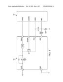
[0012]With reference first to FIG. 1, an integrated battery charger protection circuit 10 is shown in a typical mobile application such as a smart phone comprising a charge control host circuit 12. On the input side circuit 10 has a DC supply input terminal ACIN and a ground terminal GND. A charge current path runs from terminal ACIN through a protective high voltage power FET Q1 and a charge control power FET Q2 to an output terminal OUT. The gate of FET Q2 is connected to a gate drive input terminal GATDRV. Circuit 10 incorporates a low-drop linear voltage regulator LDO with a supply input connected to the tap between FETs Q1 and Q2 and a regulated voltage output connected to terminal CHGIN. A battery voltage sense terminal VBAT is a further input to circuit 10.
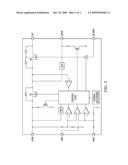
[0013]FET Q1 is driven by protective circuitry some details of which are apparent from FIG. 2.
[0014]The charge current output terminal OUT of circuit 10 is connected to a chargeable battery BAT through a resistor R1 of small value (e.g. 0.2 Ohm) and to a current sense input ISENS of circuit 12 exactly the same way as if it was connected to an external discrete charge control power FET. In fact, circuit 10 with its internal FET Q2 is "seen" by circuit 12 exactly the same as an external discrete FET of p-channel type. Likewise, circuit 12 supplies a gate drive signal on a terminal GATDRV exactly the same way as if it was intended for an external discrete charge control FET of p-channel type but, in the application shown, terminal GATDRV of circuit 12 is of course connected to terminal GATDRV of circuit 10.
[0015]Terminal CHGIN of circuit 10 is connected to a supply terminal CHGIN of circuit 12.
[0016]Both circuits 10 and 12 monitor the battery voltage. Terminal VBAT of circuit 10 is connected to the battery BAT through a resistor R2 of relatively high value (e.g. 200 kOhm) and terminal VBAT of circuit 12 is directly connected to the battery BAT.
[0017]From FIG. 2 it is seen that the gate of FET Q1 is driven by protective circuitry with a control logic and some comparators which sense the relevant voltages at various internal nodes of circuit 10. The control logic also has an input to a thermal shutdown circuit.
[0018]In operation, an external DC supply source AC is connected to terminal ACIN of circuit 10. As long as no fault condition is detected by the control logic, FET Q1 remains in an ON condition. FET Q2 receives an appropriate gate drive signal from circuit 12 which senses the voltage drop across resistor R1 due to the charge current and also senses the battery voltage. The operation of the charge control host circuit 12 is conventional and will not be disclosed further.
[0019]In the event of a failure such as an input over-voltage, a battery over-voltage, an over-current or an excessive die temperature of protective circuit 10, the control logic removes the drive signal from the gate of FET Q1, which will be blocked. The protective circuit 10 also provides a reverse current protection (short circuited charger input ACIN).
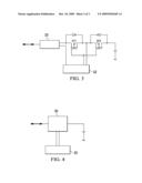
[0020]The abstract block diagrams in FIGS. 3 and 4 show a conventional bi-directional charger path solution and the inventive bi-directional charger path solution, respectively. The conventional solution uses a protective circuit 20 with an internal high voltage protective FET and a pair of discrete charge control power FETs Q11, Q12 of p-channel type driven by a charge control circuit 22. The bi-directional charge function requires a connection of the charge control circuit 22 to the node between transistors Q11 and Q12. In the inventive solution, FIG. 4, charge control FETs corresponding to the external discrete transistors Q11 and Q12 are incorporated in the integrated charge protection circuit 30, which is "seen" by the charge control circuit 32 exactly as if its internal charge control FETs were the conventional external discrete FETs.
[0021]Therefore, existing solutions are easily upgraded to higher safety standards with only minor design changes and no changes at all in the charging algorithm and software.
[0022]While the invention has been particularly shown and described with reference to preferred embodiments thereof it is well understood by those skilled in the art that various changes and modifications can be made in the invention without departing from the spirit and scope of the invention as defined by the appended claims.
User Contributions:
comments("1"); ?> comment_form("1"); ?>Inventors list |
Agents list |
Assignees list |
List by place |
Classification tree browser |
Top 100 Inventors |
Top 100 Agents |
Top 100 Assignees |
Usenet FAQ Index |
Documents |
Other FAQs |
User Contributions:
Comment about this patent or add new information about this topic:
Images included with this patent application:
 |  |
 |  |
| Similar patent applications: | |
| Date | Title |
|---|---|
| 2012-09-27 | Undervoltage protection system |
| 2009-04-16 | Overvoltage protection |
| 2011-06-09 | Over-voltage protection |
| 2013-10-31 | Electro-static discharge power supply clamp with disablement latch |
| 2013-10-31 | Electro-static discharge power supply clamp with disablement latch |
| New patent applications in this class: | |
| Date | Title |
|---|---|
| 2016-12-29 | Electrical switching apparatus including alternating current electronic trip circuit with arc fault detection circuit and power supply |
| 2016-09-01 | Limiting amplitude of electricity delivered to an electrical load |
| 2016-07-14 | Electronic device with circuit protection and assembling method thereof |
| 2016-07-07 | Power control unit with remote sensor |
| 2016-07-07 | Offset residual current protective device |
| New patent applications from these inventors: | |
| Date | Title |
|---|---|
| 2011-05-26 | Apparatus and method for impedance measurement |
| Top Inventors for class "Electricity: electrical systems and devices" | |
| Rank | Inventor's name |
|---|---|
| 1 | Zheng-Heng Sun |
| 2 | Levi A. Campbell |
| 3 | Li-Ping Chen |
| 4 | Robert E. Simons |
| 5 | Richard C. Chu |