Patent application title: POWER FACTOR CORRECTION CONTROLLER WITH DIGITAL FIR FILTER OUTPUT VOLTAGE SAMPLING
Inventors:
John L. Melanson (Austin, TX, US)
IPC8 Class: AG05F110FI
USPC Class:
323282
Class name: Output level responsive using a three or more terminal semiconductive device as the final control device switched (e.g., switching regulators)
Publication date: 2008-11-06
Patent application number: 20080272756
Inventors list |
Agents list |
Assignees list |
List by place |
Classification tree browser |
Top 100 Inventors |
Top 100 Agents |
Top 100 Assignees |
Usenet FAQ Index |
Documents |
Other FAQs |
Patent application title: POWER FACTOR CORRECTION CONTROLLER WITH DIGITAL FIR FILTER OUTPUT VOLTAGE SAMPLING
Inventors:
John L. Melanson
Agents:
HAMILTON & TERRILE, LLP
Assignees:
Origin: AUSTIN, TX US
IPC8 Class: AG05F110FI
USPC Class:
323282
Abstract:
A power control system includes a digital FIR filter in an output voltage
feedback loop of a switching power converter. A feedback loop includes an
output voltage signal of the switching power converter. The output
voltage signal includes direct current (DC) and alternating current (AC)
components. The FIR filter provides discrete samples of an output voltage
feedback signal to a switch state controller that allows the switch state
controller to generate a control signal that reflects a relatively quick
response to changes in the output voltage signal while reducing an
influence of the AC component. In at least one embodiment, the FIR filter
is configured to generate the discrete samples at a sampling frequency
fs, the sampling frequency fs is approximately an integer
multiple of a line frequency fL, and the line frequency fL is a
frequency of a line input voltage supplied to the switching power
converter.Claims:
1. An apparatus comprising:a FIR filter to generate discrete samples of an
output voltage feedback signal associated with an output voltage of a
switching power converter, wherein the FIR filter is configured to
generate the discrete samples at a sampling frequency fs, the
sampling frequency fs is approximately an integer multiple of a line
frequency fL, and the line frequency fL is a frequency of a
line input voltage supplied to the switching power converter; anda switch
state controller, coupled to the FIR filter, wherein the switch state
controller is configured to:receive a signal associated with the discrete
samples generated by the FIR filter;use the received signal to generate a
control signal to provide power factor correction and to regulate the
output voltage of the switching power converter; andprovide the control
signal to the switching power converter.
2. The apparatus of claim 1 wherein the output voltage feedback signal represents the output voltage of the switching power converter, the apparatus further comprising:an error generator coupled between the FIR filter and the switch state controller, wherein the error generator is configured to generate the signal received by the switch state controller from a difference between the discrete samples generated by the FIR filter and a reference voltage.
3. The apparatus of claim 1 further comprising:an error generator to generate the output voltage feedback signal from a difference between an output voltage of the switching power converter and a reference signal.
4. The apparatus of claim 1 wherein the FIR filter includes N taps, wherein N is an integer greater than or equal to 2, and N=fs/(2fL).
5. The apparatus of claim 4 wherein the discrete samples generated by the FIR filter have a sampling frequency in the range of the line frequency fL to Nline frequency fL wherein N is an integer equal to or greater than one.
6. The apparatus of claim 1 wherein the discrete samples generated by the FIR filter have a sampling frequency equal to the line frequency fL.
7. The apparatus of claim 1 wherein the FIR filter is a boxcar filter that includes a notch at approximately twice the line frequency fL.
8. The apparatus of claim 1 wherein the frequency fs is a member of the group consisting of (i) the line input voltage frequency, (ii) 2 times the line input voltage frequency, and (iii) 4 times the line input voltage frequency.
9. The apparatus of claim 1 wherein the FIR filter is a box car filter having a sampling frequency fs selected from the group consisting of fs=fL, fs=2fL, and fs=4fL, and a number of taps, corresponding to the sampling frequency fs, selected from the group Number of Taps as set forth in Table 2: TABLE-US-00002 Sampling Frequency fs Number of Taps fs = fL 1 fs = 2 fL 1 or 2 fs = 4 fL 1, 2, or 4
10. The apparatus of claim 1 further comprising:an input to (i) couple to an output voltage node of the switching power converter and (ii) to receive an output voltage feedback signal corresponding to the output voltage at the output voltage node; andwherein the switch state controller is further configured to:respond to changes in the output voltage feedback signal at the frequency fs.
11. The apparatus of claim 1 further comprising:a sampler to sample the output voltage at frequency fs and to generate the output voltage feedback signal.
12. The apparatus of claim 1 further comprising:an input terminal to receive a signal representing an input current to the switching power converter;wherein the switch state controller is further configured to also use the signal representing the input current to the switching power converter to generate the control signal to provide power factor correction and to regulate the output voltage.
13. A method of regulating an output voltage of a switching power converter, the method comprising:generating discrete samples of an output voltage feedback signal associated with an output voltage of a switching power converter using a FIR filter, wherein the FIR filter is configured to generate the discrete samples at a sampling frequency fs, the sampling frequency fs is approximately an integer multiple of a line frequency fL, and the line frequency fL is a frequency of a line input voltage supplied to the switching power converter;receiving a signal associated with the discrete samples generated by the FIR filter;using the received signal to generate a control signal to provide power factor correction and to regulate the output voltage of the switching power converter; andproviding the control signal to the switching power converter.
14. The method of claim 13 wherein the output voltage feedback signal represents the output voltage of the switching power converter, the method further comprising:generating the signal received by the switch state controller from a difference between the discrete samples generated by the FIR filter and a reference voltage.
15. The method of claim 13 further comprising:generating the output voltage feedback signal from a difference between an output voltage feedback signal of the switching power converter and a reference signal.
16. The method of claim 13 wherein the FIR filter includes N taps, wherein N is an integer greater than or equal to 2 and N=fs/(2fL).
17. The method of claim 16 wherein the discrete samples generated by the FIR filter have a sampling frequency in the range of the line frequency fL to Nline frequency fL.
18. The method of claim 13 wherein the discrete samples generated by the FIR filter have a sampling frequency equal to the line frequency fL.
19. The method of claim 13 wherein the FIR filter has a low pass transfer function with a notch at approximately the sampling frequency fs.
20. The method of claim 13 wherein the FIR filter is a boxcar filter that includes a notch at approximately twice the line frequency fL.
21. The method of claim 13 wherein the frequency fs is a member of the group consisting of (i) the line input voltage frequency, (ii) 2 times the line input voltage frequency, and (iii) 4 times the line input voltage frequency.
22. The method of claim 13 wherein the FIR filter is a box car filter having a sampling frequency fs selected from the group consisting of fs=fL, fs=2fL, and fs=4fL, and a number of taps, corresponding to the sampling frequency fs, selected from the group Number of Taps as set forth in the following table: TABLE-US-00003 Sampling Frequency fs Number of Taps fs = fL 1 fs = 2 fL 1 or 2 fs = 4 fL 1, 2, or 4
23. The method of claim 13 further comprising:receiving an output voltage feedback signal corresponding to the output voltage of the switching power converter;responding to changes in the output voltage feedback signal at the frequency fs.
24. The method of claim 13 further comprising:sampling the output voltage at frequency fs; andgenerating the output voltage feedback signal.
25. The method of claim 13 further comprising:receiving a signal representing an input current to the switching power converter; andusing the signal representing an input current to the switching power converter to generate the control signal to provide power factor correction and to regulate the output voltage.
26. An apparatus for regulating an output voltage of a switching power converter, the apparatus comprising:a FIR filter to generate discrete samples of an output voltage feedback signal associated with an output voltage of a switching power converter, wherein the FIR filter is configured to generate the discrete samples at a sampling frequency fs, the sampling frequency fs is approximately an integer multiple of a line frequency fL, and the line frequency fL is a frequency of a line input voltage supplied to the switching power converter;means for receiving a signal associated with the discrete samples generated by the FIR filter;means for using the received signal to generate a control signal to provide power factor correction and to regulate the output voltage of the switching power converter; andmeans for providing the control signal to the switching power converter.
Description:
CROSS-REFERENCE TO RELATED APPLICATION
[0001]This application claims the benefit under 35 U.S.C. § 119(e) and 37 C.F.R. § 1.78 of U.S. Provisional Application No. 60/915,547, filed May 2, 2007, and entitled "Power Factor Correction (PFC) Controller Apparatuses and Methods," and is incorporated by reference in its entirety.
BACKGROUND OF THE INVENTION
[0002]1. Field of the Invention
[0003]The present invention relates in general to the field of signal processing, and more specifically, to a power factor correction controller with a digital finite impulse response filter for output voltage sampling.
[0004]2. Description of the Related Art
[0005]Power control systems provide power factor corrected and regulated output voltages to many devices that utilize a regulated output voltage. FIG. 1 depicts a power control system 100, which includes a switching power converter 102. The switching power converter 102 performs power factor correction and provides constant voltage power to load 112. Voltage source 101 supplies an alternating current (AC) input voltage Vin(t) to a full, diode bridge rectifier 103. The voltage source 101 is, for example, a public utility, and the AC voltage Vin(t) is, for example, a 60 Hz/110 V line voltage in the United States of America or a 50 Hz/220 V line voltage in Europe. The rectifier 103 rectifies the input voltage Vin(t) and supplies a rectified, time-varying, line input voltage Vx(t) to the switching power converter.
[0006]The switching power converter 102 includes power factor correction (PFC) stage 124 and driver stage 126. The PFC stage 124 is controlled by switch 108 and provides power factor correction. The driver stage 126 is also controlled by switch 108 and regulates the transfer of energy from the line input voltage Vx(t) through inductor 110 to capacitor 106. The inductor current iL ramps `up` when the switch 108 conducts, i.e. is "ON". The inductor current iL ramps down when switch 108 is nonconductive, i.e. is "OFF", and supplies current iL to recharge capacitor 106. The time period during which inductor current iL ramps down is commonly referred to as the "inductor flyback time". In at least one embodiment, the switching power converter 102 operates in discontinuous current mode, i.e. the inductor current iL ramp up time plus the inductor flyback time is less than the period of switch 108.
[0007]Capacitor 106 supplies stored energy to load 112 while the switch 108 conducts. The capacitor 106 is sufficiently large so as to maintain a substantially constant output voltage Vc(t), as established by a power factor correction (PFC) and output voltage controller 114 (as discussed in more detail below). The output voltage Vc(t) remains substantially constant during constant load conditions. However, as load conditions change, the output voltage Vc(t) changes. The PFC and output voltage controller 114 responds to the changes in Vc(t) and adjusts the control signal CS0 to maintain a substantially constant output voltage as quickly as possible. The output voltage controller 114 includes a small capacitor 115 to filter any high frequency signals from the line input voltage Vx(t).
[0008]The power control system 100 also includes a PFC and output voltage controller 114 to control the switch 108 and, thus, control power factor correction and regulate output power of the switching power converter 102. The goal of power factor correction technology is to make the switching power converter 102 appear resistive to the voltage source 101. Thus, the PFC and output voltage controller 114 attempts to control the inductor current iL so that the average inductor current iL is linearly and directly related to the line input voltage Vx(t). Prodi , Compensator Design and Stability Assessment for Fast Voltage Loops of Power Factor Correction Rectifiers, IEEE Transactions on Power Electronics, Vol. 22, No. 5, September 2007, pp. 1719-1729 (referred to herein as "Prodi "), describes an example of PFC and output voltage controller 114. The PFC and output voltage controller 114 supplies a pulse width modified (PWM) control signal CS0 to control the conductivity of switch 108. In at least one embodiment, switch 108 is a field effect transistor (FET), and control signal CS0 is the gate voltage of switch 108. The values of the pulse width and duty cycle of control signal CSo depend on two feedback signals, namely, the line input voltage Vx(t) and the capacitor voltage/output voltage Vc(t).
[0009]PFC and Output Voltage Controller 114 receives two feedback signals, the line input voltage Vx(t) and the output voltage Vc(t), via a wide bandwidth current loop 116 and a slower voltage loop 118. The line input voltage Vx(t) is sensed from node 120 between the diode rectifier and inductor 110. The output voltage Vc(t) is sensed from node 122 between diode 111 and load 112. The current loop 116 operates at a frequency fc that is sufficient to allow the PFC and output controller 114 to respond to changes in the line input voltage Vx(t) and cause the inductor current iL to track the line input voltage to provide power factor correction. The current loop frequency is generally set to a value between 20 kHz and 150 kHz. The voltage loop 118 operates at a much slower frequency fv, typically 10-20 Hz. As subsequently described in more detail, the capacitor voltage Vc(t) includes an alternating current component (sometimes referred to herein as a "ripple") having a frequency equal to twice the frequency of input voltage Vin(t), e.g. 120 Hz. Thus, by operating at 10-20 Hz, the voltage loop 118 functions as a low pass filter to filter the ripple component.
[0010]FIG. 2 depicts an output voltage Vc(t) versus time graph 200. Referring to FIGS. 1 and 2, the output voltage Vc(t) supplied by power control system 100 includes a direct current (DC) component, i.e. the Vc(t) DC offset, and an alternating current (AC) component, i.e. ripple 202. The frequency fR of the ripple 202 is twice the line frequency fL of input voltage Vin(t). For example, for a line frequency fL=60 Hz, the ripple frequency fR=2fL=260 Hz=120 Hz. The Vc(t) DC offset can change over time due to input power fluctuations and load power demand fluctuations. Thus, the PFC and output voltage controller 114 monitors the output voltage Vc(t) and adjusts the control signal CS0 to return the output voltage Vc(t) to the desired value.
[0011]The ripple 202 can adversely influence the determination of the control signal CS0 by PFC and output voltage controller 114. To minimize the influence of ripple 202 on the control signal CS0, the voltage loop 118 operates at a much slower frequency fv, typically 10-20 Hz, than the line frequency fL. By operating at 10-20 Hz, the voltage loop 118 functions as a low pass filter to filter out ripple 202. However, operating at 10-20 Hz also slows the response of PFC and output voltage controller 114 to changes in the output voltage Vc(t).
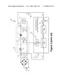
[0012]FIG. 3 depicts a generalized representation of a power control system 300 described in Prodic. The PFC and output voltage controller 302 of Prodic includes an error generator 304 to determine an error signal ed(t). The error signal ed(t) represents a difference between the output voltage Vc(t) and a reference voltage VREF. The reference voltage VREF is set to the desired value of output voltage Vc(t). A comb filter 306 filters the error signal ed(t). The comb filter 306 has significant attenuation at equally spaced frequencies (referred to as "notches") and has unity gain at other frequencies. The comb filter 306 automatically tunes the notches to match twice the line frequency fL and harmonics of the line frequency. According to Prodi , the comb filter 306 generates a "ripple free" error signal evf(t). Compensator 308 processes the filtered error signal, and input voltage feedback signal Vx(t) generates a compensator output signal. The pulse width modulator (PWM) 310 processes the compensator output signal to generate control signal CS0a.
[0013]However, it would be desirable to provide a digital pre-processing filter.
SUMMARY OF THE INVENTION
[0014]In one embodiment of the present invention, an apparatus includes a FIR filter to generate discrete samples of an output voltage feedback signal associated with an output voltage of a switching power converter. The FIR filter is configured to generate the discrete samples at a sampling frequency fs, the sampling frequency fs is approximately an integer multiple of a line frequency fL, and the line frequency fL is a frequency of a line input voltage supplied to the switching power converter. The apparatus also includes a switch state controller, coupled to the FIR filter. The switch state controller is configured to receive a signal associated with the discrete samples generated by the FIR filter and use the received signal to generate a control signal to provide power factor correction and to regulate the output voltage of the switching power converter. The switch state controller is further configured to provide the control signal to the switching power converter.
[0015]In another embodiment of the present invention, a method of regulating an output voltage of a switching power converter includes generating discrete samples of an output voltage feedback signal associated with an output voltage of a switching power converter using a FIR filter. The FIR filter is configured to generate the discrete samples at a sampling frequency fs, the sampling frequency fs is approximately an integer multiple of a line frequency fL, and the line frequency fL is a frequency of a line input voltage supplied to the switching power converter. The method further includes receiving a signal associated with the discrete samples generated by the FIR filter and using the received signal to generate a control signal to provide power factor correction and to regulate the output voltage of the switching power converter. The method also includes providing the control signal to the switching power converter.
[0016]In a further embodiment of the present invention, an apparatus for regulating an output voltage of a switching power converter includes a FIR filter to generate discrete samples of an output voltage feedback signal associated with an output voltage of a switching power converter. The FIR filter is configured to generate the discrete samples at a sampling frequency fs, the sampling frequency fs is approximately an integer multiple of a line frequency fL, and the line frequency fL is a frequency of a line input voltage supplied to the switching power converter. The apparatus also includes means for receiving a signal associated with the discrete samples generated by the FIR filter and means for using the received signal to generate a control signal to provide power factor correction and to regulate the output voltage of the switching power converter. The apparatus further includes means for providing the control signal to the switching power converter.
BRIEF DESCRIPTION OF THE DRAWINGS
[0017]The present invention may be better understood, and its numerous objects, features and advantages made apparent to those skilled in the art by referencing the accompanying drawings. The use of the same reference number throughout the several figures designates a like or similar element.
[0018]FIG. 1 (labeled prior art) depicts a power control system.
[0019]FIG. 2 (labeled prior art) depicts a power control system output voltage with an alternating current ripple component versus time graph.
[0020]FIG. 3 (labeled prior art) depicts a power and control system with an output voltage feedback filter.
[0021]FIG. 4A depicts a power control system that includes a sampling module with a digital finite impulse response (FIR) filter.
[0022]FIG. 4B depicts a graph of a boxcar FIR filter frequency response.
[0023]FIGS. 5 and 6 depict respective embodiments of the power control system of FIG. 4A.
[0024]FIG. 7 depicts a power control system that includes a sampling module with a digital FIR filter and a single feedback path.
DETAILED DESCRIPTION
[0025]A power control system includes a digital FIR filter in an output voltage feedback loop of a switching power converter. A feedback loop provides an output voltage signal of the switching power converter to a PFC and output voltage controller. The output voltage signal includes direct current (DC) and alternating current (AC) components. The FIR filter provides discrete samples of an output voltage feedback signal to a switch state controller that allows the switch state controller to generate a control signal that reflects a relatively fast response to changes in the output voltage signal while reducing an influence of the AC component on the control signal.
[0026]In at least one embodiment, the FIR filter is configured to generate the discrete samples at a sampling frequency fs, the sampling frequency fs is approximately an integer multiple of a line frequency fL, and the line frequency fL is a frequency of a line input voltage supplied by a voltage source to the switching power converter. In at least one embodiment, the sampling frequency fs is an integer multiple greater than or equal to twice the line frequency fL, and the FIR filter is a boxcar filter with a number of taps equal to fs/(2fL) and coefficients all equal to (2fL)/fs. In other embodiments, the boxcar filter has sampling frequency fs relationship to the line frequency fL and tap numbers as depicted in Table 1:
TABLE-US-00001 TABLE 1 Sampling Frequency fs Number of Taps fs = fL 1 fs = 2 fL 1 or 2 fs = 4 fL 1, 2, or 4 fs = N fL, N is an integer 1, 2, . . . , or N
[0027]The boxcar FIR filter provides attenuation ("notches") at the ripple frequency and harmonics thereof. In at least one embodiment, the boxcar FIR filter is convolved with itself, yielding a triangular FIR filter that provides even more attenuation at the ripple frequency and harmonics thereof. Increasing the number of taps of the FIR filter can reduce errors in the output samples of the FIR filter. The particular implementation of the taps is a matter of design choice. In at least one embodiment, the taps are implemented in a serial chain of sample and hold circuits, such as one D flip-flop per tap, together with coefficient multipliers (not shown) for each tap and a summation circuit connected to the output of each coefficient multiplier. In at least one embodiment, the FIR filter is implemented in software executed by a processor of, for example, PFC and output voltage controller 404 (FIG. 4A).
[0028]In at least one embodiment, the PFC and output voltage controller 404 responds to changes in the output voltage of the switching power converter at a frequency greater than or equal to the line frequency fL up to and including the sampling frequency. In at least one embodiment, the output voltage feedback signal is a direct sampled version of the switching power converter output voltage. In at least one embodiment, the output voltage feedback signal is an error signal determined from a difference between samples of the output voltage of the switching power converter and a reference signal. In at least one embodiment, the reference signal represents a desired output voltage of the switching power converter. The desired output voltage of the power control system is a design choice and depends on the voltage output demand of an intended load or loads. For example, light emitting diode fixtures can have an output voltage demand of 400 V.
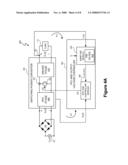
[0029]FIG. 4A depicts one embodiment of a power control system 400 that includes switching power converter 402 and a PFC and output voltage controller 404. The PFC and output voltage controller 404 includes a sampling module 408, and the sampling module 408 includes a digital FIR filter 412. In at least one embodiment, the sampling module 408 allows the PFC and output voltage controller 404 to respond to changes in the output voltage signal Vc(t) of switching power converter 402 at a frequency greater than or equal to approximately the line frequency fL up to approximately a sampling frequency fs while reducing an influence of the AC "ripple" component of the output voltage Vc(t). In at least one embodiment, the PFC and output voltage controller 302 is programmable as illustratively described in U.S. patent application entitled "Programmable Power Control System", inventor John L. Melanson, assignee Cirrus Logic, Inc., and attorney docket number 1759-CA, which is incorporated herein by reference in its entirety.
[0030]The switching power converter 402 includes a power factor correction (PFC) stage 409 to provide power factor correction. The switching power converter 402 also includes a driver stage 410 to provide a regulated output voltage Vc(t) to load 112. In at least one embodiment, PFC stage 409 and driver stage 410 are identical to respective PFC stage 124 and driver stage 126.
[0031]The PFC and output voltage controller 404 receives output voltage Vc(t) via feedback loop 412. In at least one embodiment, the output voltage Vc(t) is received from node 122 at an input terminal of PFC and output voltage controller 404. The digital FIR filter 412 filters an output voltage feedback signal. In at least one embodiment, the output voltage feedback signal is the output voltage Vc(t), and the sampled output voltage feedback signal represents the DC offset of the output voltage Vc(t). In at least one embodiment, the output voltage feedback signal is an error signal, and the sampled output voltage feedback signal is directly and linearly related to the DC offset of the output voltage Vc(t).
[0032]The output voltage feedback signal includes ripple 202. In at least one embodiment, the FIR filter 412 samples and processes the output voltage feedback signal and through significant attenuation at the ripple frequency fR and harmonics thereof effectively eliminates the frequency components of ripple 202 from the output voltage feedback signal. By attenuating the ripple 202 from a sampling module output signal VCF(n) provided from the sampling module 408 to the PFC and controller module 406, the PFC and controller module 406 can reduce the influence of ripple 202 on the determination of a control signal CS1. Additionally, the input signal to the PFC and controller module 406 is sampled at a sampling frequency fs, and, in at least one embodiment, the sampling frequency fs is equal to the line frequency fL or greater. Thus, in at least one embodiment, the PFC and controller module 406 can update the control signal CS1 at the sampling frequency fs and respond to changes in the output voltage Vc(t) at the sampling frequency fs.
[0033]Frequency fD represents an output frequency for sampling module 408 of discrete samples of the sampling module output signal VCF(n) provided to PFC and controller module 406. In at least one embodiment, the sampling frequency fs is greater than the sampling output frequency fD of discrete samples provided to PFC and controller module 406. As subsequently discussed in more detail, increasing the sampling frequency fs can reduce an error between the DC offset of the sampled output voltage feedback signal and the actual DC offset of output voltage Vc(t). However, as the sampling output frequency fD of the discrete samples increases, the response time of control signal CS1 to changes in the output voltage Vc(t) decreases. As the response time of control signal CS1 decreases, the control signal CS1 becomes more sensitive to even minor fluctuations in the power demand of load 112, which can cause, for example, oscillations in the output voltage Vc(t). Thus, the sampling output frequency fD and the corresponding response time of control signal CS1 are design choices. In at least one embodiment, the sampling output frequency fD and the response time of control signal CS1 are chosen to track the output voltage Vc(t) as accurately as possible without damaging or unnecessarily reducing the life expectancy of components of the power control system 400 and without producing oscillations of the output voltage Vc(t).
[0034]The sampling frequency fs of the FIR filter 412 is approximately an integer multiple of the line frequency fL. Unless explicitly indicated otherwise, the term "approximately" represents a nearly exact or an exact match. A value is "nearly exact" if the value achieves acceptable performance. Thus, in at least one embodiment, the sampling frequency fs=NfL, where N is any integer greater than or equal to one.
[0035]The ripple 202 is generally periodic in time. Thus, sampling the output voltage feedback signal at the line frequency fL or integer multiples thereof has the effect in the time domain of sampling the ripple 202 at the same time(s) during each period of the ripple 202. Accordingly, in the time domain, the sampled output voltage feedback signal represents a DC offset voltage of output voltage Vc(t), thus removing the ripple 202 from a feedback signal provided to PFC and controller module 406.
[0036]In at least one embodiment, the FIR filter 412 is a notch filter with significant attenuation at the sampling frequency fs and harmonics of the sampling frequency fs. The particular topology of FIR filter 412 is a matter of design choice. In at least one embodiment, the FIR filter 412 is a boxcar filter designed to provide notches at the ripple frequency fR and harmonics thereof. In at least one embodiment, the FIR filter 412 is a boxcar filter convolved with itself, yielding a triangular FIR filter, that provides even more attenuation at the ripple frequency fR and harmonics thereof.
[0037]FIG. 4B depicts a boxcar filter frequency response 450 with notches 452, 454, 456, and 458 at respective frequencies 120 Hz, 240 Hz, 360 Hz, 480 Hz, and subsequent harmonic frequencies. The boxcar filter has a sinc function and, thus, provides increasing average attenuation between notches.
[0038]As depicted in Table 1, in at least one embodiment, the FIR filter 412 has one tap and a sampling frequency fs=fL. Thus, in one embodiment, the line frequency fL=60 Hz, the ripple frequency fR=120 Hz, and the sampling frequency fs=60 Hz. Thus, the number of taps equals 1, and the coefficient equals one. Thus, a FIR filter with a sampling frequency fs=fL, simply samples the output voltage feedback signal at the line frequency.
[0039]As also depicted in Table 1, in at least one embodiment, the FIR filter 412 has one or two taps and a sampling frequency fs=2fL. In at least one embodiment, the line frequency fL=60 Hz, the ripple frequency fR=120 Hz, and the sampling frequency fs=120 Hz. The number of taps equals 1 or 2, and the coefficients equal 1 or 1/2. Thus, a FIR filter with a sampling frequency fs=2fL, simply samples the output voltage feedback signal at twice the line frequency fL with a low number of taps and coefficient multiply/add operations.
[0040]As also depicted in Table 1, in at least one embodiment, the FIR filter 412 has one, two, or four taps and a sampling frequency fs=4fL. In at least one embodiment, the line frequency fL=60 Hz, the ripple frequency fR=120 Hz, and the sampling frequency fs=240 Hz. The number of taps equals 1, 2, or 4, and the coefficients respectively equal 1, 1/2, or 1/4. Thus, a FIR filter with a sampling frequency fs=2fL, simply samples the output voltage feedback signal at twice the line frequency fL with a low number of taps and coefficient multiply/add operations.
[0041]Even if FIR filter 412 removes the frequency components of ripple 202, the ripple 202 can still adversely influence determination of the control signal CS1 because of, for example, DC offset errors in the determination of the output voltage Vc(t) from the discrete samples of FIR filter 412. For example, if the FIR filter 412 samples the output voltage feedback signal once during each period of ripple 202 and if ripple 202 is sampled at a time that does not exactly coincide with the beginning, mid-point, or end of the period (i.e. at the zero crossings relative to the actual DC offset of output voltage Vc(t)), the samples will reflect an additional DC offset equal to a difference between the DC offset of the sample and the actual DC offset of output voltage Vc(t).
[0042]In at least one embodiment, increasing the number of taps of FIR filter 412 decreases a DC offset error between discrete sample output data of FIR filter 412 and the filtered output voltage feedback signal. Additionally, increasing the number of taps smoothes transitions in the output data of FIR filter 412 as the output voltage Vc(t) changes. In at least one embodiment, FIR filter 412 has a number of taps equal to fs/(2fL), in which identical tap coefficients all equal to (2fL)/fs, and sampling frequency fs=NfL, where N is any integer greater than or equal to two. Thus, for a line frequency fL equal to 60 Hz and a sampling frequency fs equal to 120 Hz, the FIR filter 412 has notches at 120 Hz, 240 Hz, 360 Hz, and so on. For example, for an 8-tap FIR filter 412, if the line frequency fL=60 Hz, the sampling frequency fs equals 960 Hz, i.e. (8)(2)(60), and each tap coefficient is 1/8. The 8-tap FIR filter 412 removes the ripple frequency fR and harmonics thereof.
[0043]Sampling module 408 generates a discrete sampling module output signal VCF(n) at a sampling output frequency fD. As previously discussed, the sampling output frequency fD is a matter of design choice. In at least one embodiment, each sample of output signal VCF(n) of the sampling module 408 is an output of the FIR filter 412. In at least one embodiment, the output signal VCF(n) represents a moving average of the output voltage feedback signal by continuously moving samples of the output voltage feedback signal through FIR filter 412. Thus, the sampling output frequency fD equals the sampling frequency fs. In another embodiment, the FIR filter 412 processes fs/fL samples, generates an output sample of output signal VCF(n), and discards (i.e. flushes) one or more of the state variables of FIR filter 412 before proceeding to generate the next output sample VCF(n+1). If all of the state variables are discarded, the sampling output frequency fD equals the line frequency fL. Thus, by selectively discarding or keeping one or more of the state variables of FIR filter 412, the sampling output frequency fD can be the line frequency fL, the sampling frequency fs, or a frequency in between.
[0044]The PFC and output voltage controller 404 also receives signal VS(t) from switching power converter 402 via feedback loop 414. In at least one embodiment, the feedback signal VS(t) senses the rectified line input voltage Vx(t) at the input node 120. In another embodiment, the feedback signal VS(t) represents a voltage at the switch node 412. In at least one embodiment, the PFC and output voltage controller 404 can determine the line input voltage Vx(t), the output voltage Vc(t), or both from the voltage at the switch node 410 as, for example, described in the U.S. patent application entitled "Power Factor Correction Controller With Feedback Reduction", inventor John L. Melanson, assignee Cirrus Logic, Inc., and attorney docket number 1756-CA ("Melanson I") and as, for example described in the U.S. patent application entitled "Power Factor Correction Controller With Switch Node Feedback", inventor John L. Melanson, assignee Cirrus Logic, Inc., and attorney docket number 1757-CA ("Melanson II"). Melanson I and Melanson II are incorporated herein by reference in their entireties.
[0045]In embodiments of PFC and output voltage controller 404, the PFC and controller module 406 processes the feedback signal VS(t) and the input signal VCF(n) in accordance with the PFC and output voltage controllers described in Melanson I and Melanson II, with the input signal VCF(n) representing the output voltage Vc(t) in Melanson I and Melanson II. In at least one embodiment, PFC and controller module 406 processes feedback signal VS(t) and the input signal VCF(n) using the current and voltage compensators and pulse width modulator as described in Prodi .
[0046]The PFC and output voltage controller 404 can be implemented using discrete components, as one or more integrated circuits, or as a combination of discrete components and one or more integrated circuits. When implemented as one or more integrated circuits, the feedback signals VS(t) and output voltage Vc(t) can be scaled to an input voltage useable by PFC and output voltage controller 404. Exemplary sensor converters, such as voltage dividers and current sources described in Melanson I and Melanson II, can be used to scale the feedback signals VS(t) and output voltage Vc(t).
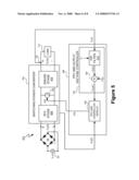
[0047]FIG. 5 depicts a power control system 500, which is one embodiment of power control system 400. The sampling module 502 represents one embodiment of sampling module 408. The output voltage Vc(t) of switching power converter 404 is fed back directly to FIR filter 412. In this embodiment, the output voltage Vc(t) represents the output voltage feedback signal referenced in conjunction with power control system 400 (FIG. 4A). FIR filter generates sampling module output signal VCF(n). An error generator 304 determines a difference between the output signal VF(n) and a reference voltage VREF by, for example, subtracting the output signal VF(n) from the reference voltage VREF. The reference voltage VREF is set to the desired value of output voltage Vc(t). Thus, since the output signal VF(n) represents the DC offset of the output voltage Vc(t), in this embodiment, the sampling module output signal VCF(n) represents an estimated error between the output voltage Vc(t) and the desired voltage value VREF.
[0048]In at least one embodiment, difficulties may arise in producing a sampling frequency fs that is an exact integer multiple of the line frequency fL. For example, if FIR filter 412 has 95 taps, the tap coefficients are all 1/95. Multiplying each sample in the FIR filter 412 by 1/95 can be a costly calculation in terms of time and implementation.
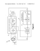
[0049]FIG. 6 depicts a power control system 600, which is one embodiment of power control system 400. The sampling module 602 represents one embodiment of sampling module 408. The output voltage Vc(t) of switching power converter 404 is fed back directly to error generator 304. Error generator 304 determines a difference signal ed(t) between the output voltage signal Vc(t) and a reference voltage VREF by, for example, subtracting the output voltage signal Vc(t) from the reference voltage VREF. In this embodiment, the difference signal ed(t) represents the output voltage feedback signal referenced in conjunction with power control system 400 (FIG. 4A). The FIR filter 412 filters the difference signal ed(t) and generates sampling module output signal VCF(n). By filtering the difference signal ed(t), the gain factor 1/(number of taps), e.g. 1/95, does not have to be as accurate as the gain factor in sampling module 602 since the output signal VCF(n) is only a feedback error value. Thus, a less costly multiplication by, for example, 1/96, for a 95 tap FIR filter 412 can be used with a negligible, if any, resulting performance loss. In at least one embodiment, an approximately 20% or less deviation in the gain factors from the ideal gain factor, i.e. 1/(number of taps), is acceptable. Since the output signal VCF(n) represents the DC offset of the output voltage Vc(t), in this embodiment, the sampling module output signal VCF(n) also represents an estimated error between the output voltage Vc(t) and the desired voltage value VREF.
[0050]FIG. 7 depicts a power control system 700. Power control system 700 is identical to power control system 400 except that the output voltage signal Vc(t) and the input voltage Vx(t) is determined from the feedback signal VS(t). The feedback signal VS(t), in the embodiment of FIG. 7, represents a voltage at the switch node 412. In at least one embodiment, the input voltage Vx(t) and output voltage Vc(t) are determined from the feedback signal VS(t) by PFC and output voltage controller 702 as described in Melanson I and Melanson II.
[0051]Thus, power control systems include a digital FIR filter. The FIR filter provides discrete samples of an output voltage feedback signal to a switch state controller that allows the switch state controller to generate a control signal that reflects a relatively quick response to changes in the output voltage signal while reducing an influence of the AC "ripple" component.
[0052]Although the present invention has been described in detail, it should be understood that various changes, substitutions and alterations can be made hereto without departing from the spirit and scope of the invention as defined by the appended claims.
User Contributions:
comments("1"); ?> comment_form("1"); ?>Inventors list |
Agents list |
Assignees list |
List by place |
Classification tree browser |
Top 100 Inventors |
Top 100 Agents |
Top 100 Assignees |
Usenet FAQ Index |
Documents |
Other FAQs |
User Contributions:
Comment about this patent or add new information about this topic:
| People who visited this patent also read: | |
| Patent application number | Title |
|---|---|
| 20220135312 | WIRELESS CONTROLLED LOCKING JAR WITH INTEGRATED VACUUM PUMP |
| 20220135311 | FOIL PACK |
| 20220135310 | INFLATION FEATURE FOR PACKAGE, INFLATION RIG ASSEMBLY, AND METHOD OF INFLATING |
| 20220135309 | PROTECTIVE ARTICLE WITH CELLULOSE-BASED EXPANDABLE COMPOSITE |
| 20220135308 | PROTECTIVE ARTICLE WITH EXPANDABLE POLYOLEFIN COMPOSITE |
Images included with this patent application:
 |  |
 |  |
 |  |
 |  |
 |
| Similar patent applications: | |
| Date | Title |
|---|---|
| 2008-11-06 | Power factor correction controller with switch node feedback |
| 2008-11-06 | Power factor correction controller with feedback reduction |
| 2011-12-15 | Current mode control of voltage regulators to mitigate output voltage ripple |
| 2008-09-04 | Method and apparatus for active power factor correction without sensing the line voltage |
| 2012-01-26 | Variable voltage converter with direct output voltage clamping |
| New patent applications in this class: | |
| Date | Title |
|---|---|
| 2022-05-05 | Semiconductor device |
| 2022-05-05 | Combined power electronics for an electric drive and a transmission control of the electric drive, inverter with such combined power electronics, electric drive with such an inverter |
| 2022-05-05 | Dual loop voltage regulator utilizing gain and phase shaping |
| 2019-05-16 | Switching circuit |
| 2019-05-16 | Power supply |
| New patent applications from these inventors: | |
| Date | Title |
|---|---|
| 2022-09-08 | Driver circuitry |
| 2022-08-25 | Driver circuitry and operation |
| 2022-08-18 | System-level chopping in coulomb counter circuit |
| 2022-08-18 | Sigma-delta modulator with residue converter for low-offset measurement system |
| 2022-08-18 | Reproducibility of haptic waveform |
| Top Inventors for class "Electricity: power supply or regulation systems" | |
| Rank | Inventor's name |
|---|---|
| 1 | Weihong Qiu |
| 2 | Benjamim Tang |
| 3 | Qian Ouyang |
| 4 | Ta-Yung Yang |
| 5 | John L. Melanson |