Patent application title: PIN TO PCB CONNECTION STRUCTURE AND METHOD
Inventors:
Jennifer L. Matoy (Leonard, MI, US)
IPC8 Class: AH05K500FI
USPC Class:
174541
Class name: With electrical device details of mount connection
Publication date: 2016-04-21
Patent application number: 20160113128
Abstract:
A printed circuit board assembly includes a printed circuit board (PCB)
having an end. The end includes surfaces defining a plurality of
electrically conductive notches therein. A plurality of electrically
conductive pins is provided with each pin being received in an associated
notch in a press-fitted manner so as to make electrical connection with
the PCB.Claims:
1. A printed circuit board assembly comprising: a printed circuit board
(PCB) having an end, the end including surfaces defining a plurality of
electrically conductive notches therein, and a plurality of electrically
conductive pins, each pin of the plurality of pins being received in an
associated notch of the plurality of notches in a press-fitted manner so
as to make electrical connection with the PCB.
2. The assembly of claim 1, wherein each pin of the plurality of pins is fixed to a housing, each pin includes a connecting portion, constructed and arranged to be connected with a mating electrical connector, and an engaging portion engaged with the associated notch.
3. The assembly of claim 3, wherein the engaging portion is disposed generally 90.degree. with respect to the connecting portion.
4. The assembly of claim 2, wherein the connecting portion and the engaging portion are both on the same axis.
5. The assembly of claim 3, wherein each pin of the plurality of pins is press-fitted into the housing.
6. The assembly of claim 3, wherein each pin of the plurality of pins is molded into the housing.
7. A printed circuit board assembly comprising: a printed circuit board (PCB) having an end, the end including surfaces defining a plurality of electrically conductive notches therein, a plurality of electrically conductive pins, each pin of the plurality of pins being received in an associated notch of the plurality of notches in a press-fitted manner so as to make electrical connection with the PCB, and a housing receiving the PCB, the plurality of pins being mounted to the housing.
8. The assembly of claim 7, wherein each pin of the plurality of pins is press-fitted into the housing.
9. The assembly of claim 7, wherein each pin of the plurality of pins is molded into the housing.
10. The assembly of claim 7, wherein each pin of the plurality of pins includes a connecting portion, constructed and arranged to be connected with a mating electrical connector, and an engaging portion engaged with the associated notch.
11. The assembly of claim 10, wherein the engaging portion is disposed generally 90.degree. with respect to the connecting portion.
12. A method of connecting pins to a printed circuit board, the method comprising the steps of: providing a plurality of electrically conductive notches in an end of a printed circuit board (PCB), providing a plurality of electrically conductive pins so that each pin aligns with an associated notch, and moving the PCB or the plurality of pins so that each pin engages the associated notch in a press-fitted manner so as to make electrical connection with the PCB.
13. The method of claim 12, wherein the step of providing the plurality of pins includes mounting the pins to a housing.
14. The method of claim 12, wherein the step of moving includes moving the PCB with respect to the housing.
15. The method of claim 14, wherein the step of moving the PCB includes sliding the PCB, along a longitudinal axis thereof into engagement with the pins.
16. The method of claim 14, wherein the step of moving the PCB includes moving the PCB, in a direction transverse to a longitudinal axis thereof, into engagement with the pins.
17. The method of claim 12, wherein the step of moving includes moving the pins into engagement with the notches.
18. The method of claim 12, wherein the mounting step includes press-fitting the pins into the housing.
19. The method of claim 12, wherein mounting step includes molding the pins into the housing.
Description:
FIELD
[0001] The invention relates to a printed circuit boards (PCB) and connector pins and, more particularly, to the ability to directly connect the pins to the PCB without the use of a pin header.
BACKGROUND
[0002] With reference to FIG. 1, a typical PCB 10 includes a plastic pin header 12 with pins 14 bent at a 90° angle. The pin header 12 is wave soldered to the PCB 10 to make a 90° connection. The PCB 10 is received in a housing 16, typically made of plastic. It was contemplated to use a reflow soldering process to solder the pins 14 to the PCB 10. However, since a reflow soldering process involves the parts going through an oven, the plastic pin header 12 would melt unless specifically designed for this process.
[0003] Thus, there is a need to connect pins directly to a PCB without the use of a pin header.
SUMMARY
[0004] An objective of the invention is to fulfill the need referred to above. In accordance with the principles of an embodiment, this objective is obtained by providing a printed circuit board assembly that includes a printed circuit board (PCB) having an end. The end includes surfaces defining a plurality of electrically conductive notches therein. A plurality of electrically conductive pins is provided with each pin being received in an associated notch in a press-fitted manner so as to make electrical connection with the PCB.
[0005] In accordance with another aspect of an embodiment, a method connects pins to a printed circuit board. The method provides a plurality of electrically conductive notches in an end of a printed circuit board (PCB). A plurality of electrically conductive pins is provided so that each pin aligns with an associated notch. The PCB or the plurality of pins is moved so that each pin engages the associated notch in a press-fitted manner so as to make electrical connection with the PCB.
[0006] Other objectives, features and characteristics of the present invention, as well as the methods of operation and the functions of the related elements of the structure, the combination of parts and economics of manufacture will become more apparent upon consideration of the following detailed description and appended claims with reference to the accompanying drawings, all of which form a part of this specification.
BRIEF DESCRIPTION OF THE DRAWINGS
[0007] The invention will be better understood from the following detailed description of the preferred embodiments thereof, taken in conjunction with the accompanying drawings, wherein like reference numerals refer to like parts, in which:
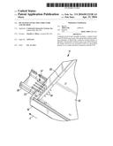
[0008] FIG. 1 is view of a conventional PCB having a plastic pin header and pins wave soldered to the PCB, with the PCB shown disposed in a housing.
[0009] FIG. 2 is a partial view of a PCB assembly showing a PCB being inserted into a housing to engage pins in accordance with an embodiment.
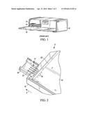
[0010] FIG. 3 is a view showing the pins of FIG. 2 engaged with notches in the PCB.
[0011] FIG. 4 is a top view of the pins of the embodiment engaged in the notches of the PCB.
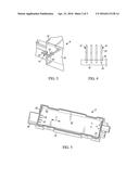
[0012] FIG. 5 is a view of the PCB assembly of an embodiment shown in an assembled condition.
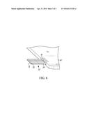
[0013] FIG. 6 is a view of an embodiment of straight pins press-fitted into notches of the PCB of FIG. 2.
DETAILED DESCRIPTION OF EXEMPLARY EMBODIMENTS
[0014] With reference to FIG. 2, a printed circuit board (PCB) assembly is shown, generally indicated at 11, in accordance with an embodiment. The assembly 11 includes a PCB 10' that has surfaces defining a plurality of slots or notches 18 in the end 20 of the PCB 10' on the side where the PCB 10' is inserted into a housing 16'. Each notch 18 is electrically conductive so as to power the PCB once connected with an associated electrically conductive pin, generally indicated at 14'.
[0015] A plurality of electrically conductive pins, generally indicated at 14', is mounted to the housing 16' in a molded or press fitted manner. Each pin 14' can be an individual pin that is then molded or press fitted into the housing 16' so as to align with an associated notch 18. This configuration eliminates the need for the pin header 12 of FIG. 1. Each pin 14' has a connecting portion 22, constructed and arranged to be connected with a mating electrical connector (not shown), and an engaging portion 24 preferably disposed generally 90° with respect to the connecting portion 22. When the PCB 10' is moved in the direction of arrow A in FIG. 2, each engaging portion 24 is received in and engages an associated notch 18 in the PCB 10 in a press-fitted manner, as shown in FIGS. 3 and 4. This press fit area of the pins 14' to the PCB 10' does not require significant force as long as electrical connection is made, since the housing 16' and cover (not shown) will hold the PCB 10' from moving. When the electrical connector (not shown) is inserted into the connector housing 26, the stress is no longer transferred to the PCB 10' because the pins 14' are held in by the housing 16'.
[0016] With the pins 14' molded or fitted into the housing 16' and engaged in a press-fitted manner with the PCB 10', space on the PCB 10' can be saved. Also, the plastic pin header of the prior art configuration can be eliminated along with the cost of tooling the pin header.
[0017] Although the pins 14' are shown to be bent 90° degrees, with reference to FIG. 6, the pins 14'' can be straight pins, with an end opposite the connecting portion 22 defining the engaging portion 24 of each pin 14''. Thus, the connecting portion 22 and the engaging poring 24 are both on the same axis B. The straight pins 14'' would require a less expensive stamping.
[0018] With reference to FIG. 5, instead of sliding the PCB 10' along the longitudinal axis C into the housing, the PCB 10' can be pressed down (in a direction transverse to the longitudinal axis C) into the housing 16' to engage the pins 14'. In another embodiment, instead of providing the pins 14' in the housing 16', the pins 14' can be considered to be part to the electrical connector (not shown) that is inserted into the connector housing 26, such that once inserted therein, the pins of the electrical connector engage the notches 18 in the manner discussed above.
[0019] The foregoing preferred embodiments have been shown and described for the purposes of illustrating the structural and functional principles of the present invention, as well as illustrating the methods of employing the preferred embodiments and are subject to change without departing from such principles. Therefore, this invention includes all modifications encompassed within the spirit of the following claims.
User Contributions:
Comment about this patent or add new information about this topic:
Images included with this patent application:
 |  |
 |  |
| New patent applications in this class: | |
| Date | Title |
|---|---|
| 2016-07-07 | Laundry treatment apparatus and door thereof |
| 2016-04-14 | Push-in cable connector and electrical box assembly |
| 2016-04-14 | Electrical junction box |
| 2016-02-18 | Leakage-blocking structure, electronic component, and electronic component unit |
| 2016-02-18 | Electronic component unit |
| Top Inventors for class "Electricity: conductors and insulators" | |
| Rank | Inventor's name |
|---|---|
| 1 | Douglas B. Gundel |
| 2 | Shou-Kuo Hsu |
| 3 | Michimasa Takahashi |
| 4 | Hideyuki Kikuchi |
| 5 | Tsung-Yuan Chen |