Patent application title: P-Type Transition Metal Oxide-Based Films Serving as Hole Transport Layers in Organic Optoelectronic Devices
Inventors:
Xiong Gong (Hudson, OH, US)
Tingbin Yang (Akron, OH, US)
Assignees:
THE UNIVERSITY OF AKRON
IPC8 Class: AH01L5100FI
USPC Class:
438 47
Class name: Making device or circuit emissive of nonelectrical signal compound semiconductor heterojunction
Publication date: 2014-10-02
Patent application number: 20140295604
Abstract:
An improvement in a method of making a semiconducting device having a
hole-collecting electrode includes coating the hole-collecting electrode
with a p-type transition metal oxide through a sol-gel process.Claims:
1. In a method of making a semiconducting device having a hole-collecting
electrode, the improvement comprising: coating the hole-collecting
electrode with a p-type transition metal oxide through a sol-gel process.
2. In the method of claim 1, wherein the p-type transition metal oxide is selected from MoO3, V2O5, NiO, and WO.sub.3.
3. In the method of claim 2, wherein the semiconducting device is an organic optoelectronic device.
4. In the method of claim 3, wherein the organic optoelectronic device is selected from photovoltaic cells, light emitting diodes, and photodetectors.
5. In the method of claim 4, wherein the organic optoelectronic device is bulk heterojunction photovoltaic cell.
6. In the method of claim 5, wherein the bulk heterojunction photovoltaic cell includes a heterojunction active layer including a polymer blend of electron donor and electron acceptor material.
7. In the method of claim 6, wherein the electron donor is PBDT-DTNT and the electron acceptor is PC71-BM.
8. In the method of claim 7, wherein the hole-collecting electrode is indium-tin-oxide.
9. In the method of claim 8, wherein the heterojunction photovoltaic cell includes an aluminum electron-collecting electrode.
10. In the method of claim 9, wherein the p-type transition metal oxide is MoO.sub.3.
11. In the method of claim 2, wherein the wherein the p-type transition metal oxide is MoO.sub.3.
12. A method for manufacturing a solar cell, the method comprising: providing an anode; providing an active layer including a polymer; providing a cathode; coating the anode with a p-type transition metal oxide thin film derived from sol-gel process.
13. The method of claim 12, wherein the transition metal oxide thin film is selected from MoO3, V2O5, NiO, and WO.sub.3.
14. The method of claim 12, wherein the transition metal oxide thin film is MoO.sub.3.
15. The method of claim 14, wherein the anode is indium-tin-oxide, and the active layer is a polymer blend of PBDT-DTNT and PC71-BM.
Description:
CROSS-REFERENCE TO RELATED APPLICATIONS
[0001] The present application claims the benefit of U.S. Provisional Patent Application No. 61/551,958, filed Oct. 27, 2011.
FIELD OF THE INVENTION
[0002] The present invention generally relates to hole transport layers for semiconducting devices. More particularly, the present invention relates to sol-gel methods of deposition of hole transport layers on an electrode of such devices.
BACKGROUND OF THE INVENTION
[0003] Bulk heterojuction (BHJ) polymer solar cells (PSCs) based on conjugated polymers (electron donor (D)) blended with fullerene derivatives (electron acceptors (A)) have attracted great attention due to their potential as renewable energy sources, and the advantages of easy processing and the possibility to fabricate inexpensive, light weight flexible devices. Power conversion efficiency (PCE) of over 8% have been reported for BHJ PSCs under AM1.5G with an illuminating intensity of 100 mW/cm2. However, the major challenge for BHJ PSCs is the demonstration of long-term air stability.
[0004] BHJ PSCs are typically fabricated with a transparent conductive anode (e.g. indium tin oxide (ITO)), a low-work-function metal cathode(e.g. Al, Ba/Al and Ca/Ag (Al)), and an active layer (D:A) sandwiched between the anode and the cathode. The cathode is inherently flawed in lower long-term stability. Poly(3,4-ethylenedioxythiophene):poly(styrene sulfonate) (PEDOT:PSS) is often used to smooth the surface of anode, ITO. However, it has been demonstrated that long-term stability is a problem because PEDOT:PSS is hygroscopic and acidic in nature. PEDOT:PSS will etch the ITO, in particular, at ambient condition and accelerate indium diffusing into photoactive layer, then induce a fast degradation of active layer.
[0005] Two approaches have been developed to circumvent these problems. One is to develop BHJ PSCs with an inverted device structure. Another is to introduce a stable buffer layer to replace the PEDOT:PSS. Recently, metal oxides, such as molybdenum oxide (MoO3), vanadium pentoxide (V2O5) are thermally deposited onto the ITO anode as a hole transport layer. The elimination of the PEDOT:PSS layer improves the device stability.
[0006] Notably, thermal deposition requires the use of complex and expensive equipment, including vacuum chambers and high temperatures, for deposition of the metal oxide on the substrate. High temperature and thus high energy is required to vaporize the solid metal sample. Thus, there is a need in the art for a sol-gel method for thin film deposition of MoO3 in BHJ PSCs. This need extends more generally to sol-gel thin film deposition of hole transport layers of other p-type metal oxides in other semiconductor devices.
SUMMARY OF THE INVENTION
[0007] In a first embodiment, this invention provides an improvement in a method of making a semiconducting device having a hole-collecting electrode, the improvement comprising: coating the hole-collecting electrode with a p-type transition metal oxide through a sol-gel process.
[0008] In a second embodiment, this invention provides a method as in the first embodiment, wherein the p-type transition metal oxide is selected from MoO3, V2O5, NiO, and WO3.
[0009] In a third embodiment, this invention provides a method as in the first or second embodiments, wherein the semiconducting device is an organic optoelectronic device.
[0010] In a fourth embodiment, this invention provides a method as in any of the first through third embodiments, wherein the organic optoelectronic device is selected from photovoltaic cells, light emitting diodes, and photodetectors.
[0011] In a fifth embodiment, this invention provides a method as in any of the first through fourth embodiments, wherein the organic optoelectronic device is bulk heterojunction photovoltaic cell.
[0012] In a sixth embodiment, this invention provides a method as in any of the first through fifth embodiments, wherein the bulk heterojunction photovoltaic cell includes a heterojunction active layer including a polymer blend of electron donor and electron acceptor material.
[0013] In a seventh embodiment, this invention provides a method as in any of the first through sixth embodiments, wherein the electron donor is PBDT-DTNT and the electron acceptor is PC71-BM.
[0014] In an eighth embodiment, this invention provides a method as in any of the first through seventh embodiments, wherein the hole-collecting electrode is indium-tin-oxide.
[0015] In a ninth embodiment, this invention provides a method as in any of the first through eighth embodiments, wherein the heterojunction photovoltaic cell includes an aluminum electron-collecting electrode.
[0016] In a tenth embodiment, this invention provides a method as in any of the first through ninth embodiments, wherein the p-type transition metal oxide is MoO3.
[0017] In an eleventh embodiment, this invention provides a method as in any of the first through third embodiments, wherein the wherein the p-type transition metal oxide is MoO3.
[0018] In a twelfth embodiment, this invention provides a method for manufacturing a solar cell, the method comprising: providing an anode; providing an active layer including a polymer; providing a cathode; coating the anode with a p-type transition metal oxide thin film derived from sol-gel process.
[0019] In a thirteenth embodiment, this invention provides a method as in the twelfth embodiment, wherein the transition metal oxide thin film is selected from MoO3, V2O5, NiO, and WO3.
[0020] In a fourteenth embodiment, this invention provides a method as in either of the twelfth or thirteenth embodiments, wherein the transition metal oxide thin film is MoO3.
[0021] In a fifteenth embodiment, this invention provides a method as in any of the twelfth through fourteenth embodiments, wherein the anode is indium-tin-oxide, and the active layer is a polymer blend of PBDT-DTNT and PC71-BM.
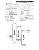
BRIEF DESCRIPTION OF THE DRAWINGS
[0022] FIG. 1 shows the molecular structures of PBDT-DTNT and PC71BM.
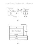
[0023] FIG. 2 shows the device structure of a polymer solar cell created per the example section herein.
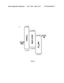
[0024] FIG. 3 shows an energy-level diagram showing the LUMO and HOMO of each component of the polymer solar cell of the example section.
[0025] FIG. 4 is a graph showing the absorption spectrum of the solution-processed MoO3 thin film annealed at 250° C. as per the example section.
[0026] FIG. 5 is a graph showing the x-ray photoelectron spectrum of solution-processed MoO3 thin film on top of the ITO substrate annealed at 250° C. as per the example section.
[0027] FIG. 6 is a graph showing the core level of Mo 3 d.
[0028] FIG. 7 is a graph showing the core level of O 1 s.
[0029] FIG. 8 shows TEM images of the solution-processed MoO3 after annealed at 250° C.
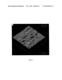
[0030] FIG. 9 shows Tapping-Mode AFM images of the solution-processed MoO3 thin film annealed at 250° C., with a RMS of 0.457 nm.
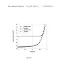
[0031] FIG. 10 is a graph showing J-V characteristics of polymer solar cells incorporated with a solution-processed MoO3 and a PEDOT:PSS layer.
DETAILED DESCRIPTION OF ILLUSTRATIVE EMBODIMENTS
[0032] The present invention provides a method of depositing hole transport layers on a hole-collecting electrode in a semiconducting device. Herein, a "semiconducting device" includes any device including a semiconducting material and a hole-collecting electrode.
[0033] In some embodiments, the semiconducting device is selected from organic optoelectronic devices. In some embodiments, the semiconducting device is an organic optoelectronic device selected from photovoltaic cells, light emitting diodes, and photodetectors. In some embodiments the semiconducting device is a thin film transistor.
[0034] In some embodiments, the semiconducting device is a photovoltaic cell selected from single layer photovoltaic cells, bilayer photovoltaic cells and heterojunction photovoltaic cells. In some embodiments, the photovoltaic cell is a heterojunction photovoltaic cell selected from bulk heterojuction photovoltaic cells and graded heterojunction photovoltaic cells.
[0035] In some embodiments the semiconducting device is an organic light emitting diode.
[0036] In some embodiments, the semiconducting device is a photodetector device selected from active pixel sensors, photodiode light sensors, light dependent resistors,
[0037] In some embodiments, the semiconducting device is an active pixel sensor selected from charged-coupled device sensors (CCD sensors) and complementary metal-oxide-semiconductor sensors (CMOS sensors).
[0038] In some embodiments the semiconducting device is a thin film transistor.
[0039] The hole transport layer is a p-type transition metal oxide. In some embodiments the p-type transition metal oxide is selected from MoO3, V2O5, NiO, and WO3. In some embodiments, the p-type transition metal oxide is molybdenum trioxide (MoO3). In some embodiments, the p-type metal oxide is tungsten trioxide (WO3). In some embodiments, the p-type metal oxide is vanadium pentoxide (V2O5). In some embodiments, the p-type metal oxide is nickel(II) oxide (NiO).
[0040] In this invention, a p-type transition metal oxide film is formed on the hole-collecting electrode of the semiconducting device through a sol-gel process that employs a low annealing temperature. This is beneficial from a manufacturing standpoint, particularly as compared to thermal deposition techniques of the prior art.
[0041] To form the p-type metal oxide on the hole-collecting electrode, a colloidal metal-oxide precursor (sol) is first formed. It should be noted that it is possible to obtain the desired metal oxide already prepared, thereafter forming the metal-oxide precursor. However, the metal oxide might be prepared by oxidation of the base metal through known or developed processes. Regardless, an appropriate solvent is employed to create the colloidal precursor, and the colloidal metal-oxide precursor is then deposited as a coating on a semiconducting device and annealed to form the desired film (gel).
[0042] In a particular embodiment, the metal-oxide precursor is a molybdenum-oxide precursor. Though the molybdenum trioxide can be obtained from any commercial source, it may also be formed by mixing molybdenum powder with hydrogen peroxide to form molybdenum trioxide (MoO3) and water:
Mo+H2O2═MoO3+H2O
[0043] The solution may need to be centrifuged to remove residual Mo metal. The solution is then dried to obtain the molybdenum trioxide, which is then dissolved in methanol. This resulting MoO3 precursor can then be used as a coating on a hole-collecting electrode of a semiconducting device.
[0044] Once prepared, the colloidal metal oxide precursor is used to coat the hole-collecting electrode. The colloidal metal oxide precursor can be coated onto the hole-collecting electrode by any suitable method known to those of skill in the art. In particular embodiments the coating is formed through a spin-casting process.
[0045] In some embodiments, the colloidal metal-oxide precursor is deposited at a thickness of from 10 nanometers (nm) or greater to 200 nm or less. In other embodiments, the colloidal metal-oxide precursor is deposited at a thickness of from 20 nm or greater to 100 nm or less, in other embodiment, from 25 nm or greater to 50 nm or less, and, in other embodiments, from 25 nm or greater to 35 nm or less. In some embodiments, the colloidal metal-oxide precursor is deposited at a thickness greater than or equal to 10 nm, in other embodiments, 15 nm, in other embodiments, 20 nm, in other embodiments, 25 nm and, in other embodiments, 30 nm. In some embodiments, the colloidal metal-oxide precursor is deposited at a thickness less than or equal to 200 nm, in other embodiments, 150 nm, in other embodiments, 100 nm, in other embodiments, 50 nm and, in other embodiments, 40 nm.
[0046] In some embodiments, the colloidal metal-oxide precursor is a colloidal MoO3 precursor, as above, and is coated onto a hole-collecting electrode of a semi-conducting device. In other embodiments, the colloidal metal-oxide precursor is a colloidal MoO3 precursor, as above, and is coated onto a hole-collecting electrode of a bulk heterojunction photovoltaic cell.
[0047] In a particular embodiment, the colloidal metal-oxide precursor is a colloidal MoO3 precursor, as above, and it is spin cast onto a hole-collecting electrode. In a specific embodiment, a colloidal MoO3 precursor, as above, is spin cast onto a hole-collecting electrode of a bulk heterojunction photovoltaic cell.
[0048] The deposited coating of metal-oxide precursor is thermally annealed to form the desired transition metal oxide film. The annealing creates the desire metal-oxide thin film on the hole-collecting electrode, the metal-oxide film serving as a hole transport layer.
[0049] In some embodiments, the colloidal metal-oxide precursor is a colloidal MoO3 precursor, and the deposited coating is annealed at a temperature of from 225° C. or greater to 300° C. or less. In other embodiments, the annealing temperature is from 225° C. or greater to 275° C. or less. In a particular embodiment, the annealing temperature is 250° C.
[0050] In some embodiments, the deposited coating is annealed at a temperature greater than or equal to 225° C., in other embodiments greater than or equal to 250° C. In some embodiments, the deposited coating is annealed at a temperature less than or equal to 300° C., in other embodiments less than or equal to 275.° C.
[0051] In some embodiments, the deposited coating is annealed for a period of time of 20 minutes or greater to 60 minutes or less. In other embodiments the deposited coating is annealed for period of time of 25 minutes or more to 35 minutes or less.
[0052] Having coated the hole-collecting electrode with the hole-transport layer of metal-oxide, the semiconducting device can be manufactured in accordance with general knowledge in the art. Indeed, the hole-colleting electrode may be coated by the present process at any practical time during the manufacturing process.
[0053] In some embodiments, the semiconducting device is a bulk heterojunction photovoltaic cell, and, after the hole-collecting layer is coated with the hole-transport layer, the electron donor/electron acceptor polymer blend of the heterojuction is coated onto the metal-oxide hole transport layer. Thereafter, the heterojunction is annealed, and a final electron-accepting electrode can be deposited on the heterojunction to complete the cell.
[0054] In a particular embodiment, the semiconducting device is a bulk heterojunction photovoltaic cell. The heterojunction active layer is a polymer blend of electron donor and electron acceptor material. The electron donor material may be selected from virtually any electron donor material useful in heterojunction photovoltaic cells. The electron acceptor material may be selected from virtually any electron acceptor material useful in heterojunction photovoltaic cells. In a specific embodiment, the polymer blend is PBDT-DTNT and PC71-BM.
[0055] The bulk heterojunction photovoltaic cell includes a hole-collecting electrode and an electron-collecting electrode. The hole-collecting electrode may be formed of virtually any hole-collecting electrode material useful in heterojunction photovoltaic cells. The electron collecting electrode may be formed of virtually any electron-collecting electrode material useful in heterojunction photovoltaic cells. In a particular embodiment, the hole-collecting electrode material is ITO. In another embodiment, the electron-collecting electrode material is selected from aluminum magnesium and calcium. In a specific embodiment, the hole-collecting electrode material is ITO and the electron-collecting electrode material is aluminum.
[0056] In accordance with this invention, the bulk heterojunction photovoltaic cell layer includes a hole transport layer as taught herein. In a particular embodiment, the hole transport layer is MoO3. The MoO3 layer is coated onto the hole-collecting electrode. The electron donor/electron acceptor polymer blend of the heterojuction is coated onto the metal-oxide hole transport layer. Thereafter, the heterojunction is annealed, and a final electron-accepting electrode is deposited on the heterojunction to complete the cell.
[0057] In a specific embodiment, the semiconducting device is a bulk heterojunction photovoltaic cell, The hole-collecting electrode is ITO, the electron-collecting electrode is aluminum, the bulk heterojunction is PBDT-DTNT:PC71BM, and the hole transport layer is MoO3, the precursor being formed and cast and then annealed as described above. Further details are found in the specific examples provided below.
[0058] In light of the foregoing, it should be appreciated that the present invention significantly advances the art by providing a method for hole transport layer deposition on a hole-collecting electrode of a semiconducting device.
EXAMPLE
Introduction
[0059] The molecular structures of PBDT-DTNT and [6,6]-phenyl C71-butyric acid methyl ester (PC71BM) are shown in FIG. 1. The bulk heterojunction (BHJ) polymer solar cell (PSC) structure is shown in FIG. 2. The energy levels of the component materials are shown in FIG. 3. Sol-gel derived MoO3 films were prepared using molybdenum in H2O2 as a precursor solution. The details of synthesis are described in the Experimental Section, below. The precursor solution was cast onto ITO-glass and subsequently treated at different temperatures for 30 minutes. During this time period the precursor was converted to dense MoO3 film by hydrolysis. The UV-visible absorption spectrum of solution-processed MoO3 thin film following thermally annealing at 250° C. for 30 minutes is shown in the graph of FIG. 4. The bandgap of MoO3 film obtained from UV-visible spectrum is ˜3.0 eV. It can be seen from FIG. 4 that the MoO3 film is transparent from 400 nm to 1000 nm. This character indicated that MoO3 film can be a buffer layer onto ITO-glass allowing all visible light to pass through both the ITO and MoO3 layer and into the polymer active layer (heterojunction). As shown in FIG. 3, because the highest occupied molecular orbital (HOMO) of MoO3 is close to that of PBDT-DTNT, holes can be efficiently transported to the ITO anode without significant loss in energy. Moreover, because the lowest unoccupied molecular orbital (LUMO) of MoO3 is higher than that of PBDT-DTNT, MoO3 film can be functionalized as electron blocking layer.
[0060] X-ray photoelectron spectroscopy (XPS) measurements were made n order to characterize the composition of sol-gel derived MoO3 film. FIGS. 6 and 7 show core level XPS spectra of Mo 3 d and O 1 s for the sol-gel derived MoO3 films annealed at 250° C. XPS spectra are referenced to the residual hydrocarbon contamination at 284.6±0.1 eV. The whole spectrum of MoO3 (FIG. 5) shows five sharp peaks. The C 1 s peak from the experimental data is located at 281.7 eV, which is about 2.9 eV less than the referenced value, indicating that the other peak positions need to be calibrated by adding this offset. Table 1 summarizes the details of the peak offsets. The binding energies for Mo (3d5/2) and Mo (3d3/2) are 232.5 eV and 235.6 eV, respectively. The binding energy of 232.5 eV corresponds to the oxide of Mo (VI). All these data demonstrated the major component in sol-gel derived MoO3 film is MoO3.
TABLE-US-00001 TABLE 1 XPS binding energy of Molybdenum compound Item C 1s O 1s Mo 3d5/2 Mo 3d 3/2 Mo 3p3/2 Exp. Data 281.7 527.6 229.6 232.7 395.4 Calibrated 284.6 530.5 232.5 235.6 398.3
[0061] The tuning position of O 1 s is at 530.5 eV. However, several O 1 s peaks could be fitted from core level of O 1 s spectra which indicated that more than one oxygen species was present in MoO3 film. Moreover, the peak located at 398.3 eV from core level of Mo 3p3/2, is corresponding to state of Mo (VI). All these results further demonstrated that major component of sol-gel derived MoO3 was formed to MoO3.
[0062] FIG. 8 shows the transmission electron microscopy (TEM) of the MoO3 thin film annealed at 250° C. It can be seen that the MoO3 thin film is quite uniform. Nanoscale fibrils with a diameter of ˜20 nm were observed. No visible pinhole was present in this TEM image. This implied that the thin film was quite dense, preventing current leakage that might occur due to incomplete cover the ITO substrate. An atomic force microscopy (AFM) height image is depicted in FIG. 9, with a root mean roughness (RMS) of 0.475 nm at a scale of 2.0 μm×2.0 μm. This smooth surface of solution-processed MoO3 films offers a good surface to deposit the top photoactive layer. In addition, the typical sharp peak of the ITO substrate was not observed when spin-casting a layer of MoO3, indicating that the rough surface of the ITO had been modified. These results indicated that solution-processed MoO3 has good morphology as a buffer layer in BHJ PSCs.
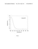
[0063] The current-density voltage characteristics (J-V) of the BHJ PSCs incorporated with a sol-gel derived MoO3 is shown in FIG. 10. A PCE of 5.86% was obtained under AM1.5G with light intensity of 100 mW/cm2. BHJ PSCs with sol-gel derived MoO3, the open-circuit voltage (Voc) was 0.75 V, short-circuit current density (Jsc) was 16.44 mA/cm2 and fill factor was 47.5%. Dark J-V characteristics were also plotted in FIG. 10. The rectification at ±1 V was close to 104, indicating a good diode performance. A high Voc observed from BHJ PSCs with sol-gel derived MoO3 suggested a good band alignment between active layer and electrodes. The small difference in the calculated Voc (0.89V) and observed Voc (0.75 V) implied that only 0.14 V was lost even the electrode contact resistance involved. A high Jsc observed from BHJ PSCs with sol-gel derived MoO3 indicated that the charge transport across the MoO3 layer was unhindered. In order to confirm it, BHJ PSCs with PEDOT:PSS as a buffer layer was also investigated. A PCE of 5.89%, a Voc of 0.73 V, a Jsc of 16.64 mA/cm2 and a FF of 48.5% were observed. All these device performance parameters are comparable with those observed from BHJ PSCs with sol-gel derived MoO3. Therefore, this example demonstrates that sol-gel derived MoO3 can be used as a hole transporting layer for approaching high performance BHJ PSCs.
[0064] In conclusion, sol-gel derived MoO3 as a hole transport layer in bulk heterojunction polymer solar cells was demonstrated. A power conversion efficiency of 5.86% was observed from BHJ PSCs with a device structure of ITO/S-MoO3/PBDT-DTNT:PC71BM/Al. This value is comparable with the power conversion efficiency (5.89%) obtained from BHJ PSCs with a device structure of ITO/PEDOT:PSS/PBDT-DTNT:PC71BM/Al. Characterization of sol-gel derived MoO3 films was carried out by x-ray photoelectron spectrum, absorption spectrum, transmitted electron microscopy, atomic force microscopy. All these results demonstrated that sol-gel derived MoO3 can be used as a hole transporting layer for approaching high performance BHJ PSCs.
[0065] Experimental Section
[0066] Materials
[0067] PBDT-DTNT was synthesized by Wang et al. recently. PC71BM and Molybdenum powder were purchased from Aldrich. Methanol was purchased from Guangzhou Chemical Reagent Factory.
[0068] MoO3 Preparation
[0069] Molybdenum power (10 g) was first prepared in a clean beaker, then a 100 mL H2O2 (Concentration: 30%) was slowly added into this beaker. To avoid a great deal of heat, a cool water bath was needed. The above solution was centrifuged at a rate of 3000 rpm to remove the rudimental substance. The solution was subsequently dried by distillation. The resulting product was then dissolved in methanol with a concentration of 10 mg/mL for preparation of the MoO3 thin film.
[0070] Characterization of MoO3
[0071] UV-Visible Absorption Spectrum
[0072] The UV-visible absorption spectrum of sol-gel derived MoO3 was measured by a HP 8453 UV-vis spectrophotometer.
[0073] X-Ray Photoelectron Spectrum (XPS)
[0074] XPS analysis was carried out on an X-ray Photoelectron Spectroscopy/ESCA (Model: Axis Ultra DLD, Kratos Inc.) utilizing a monochromatized Al Kα X-ray source. Spectra are referenced to the residual hydrocarbon contamination at 284.6±0.1 eV. Thin films (˜30 nm) were deposited on the ITO substrate for XPS analysis.
[0075] Morphologies
[0076] Transmission electron microscopy (TEM) experiments were carried out with a Philips Tecnai 12 using an accelerating voltage of 120 kV. Tapping-mode atomic force microscopy (AFM) images were obtained using a NanoScope NS3A system (Digital Instrument) to observe the surface morphology of MoO3.
[0077] Device Fabrication
[0078] For comparison, the following BHJ PSCs were fabricated: ITO/MoO3/PBDT-DTNT:PC71BM/Al and ITO/PEDOT:PSS/PBDT-DTNT:PC71BM/Al. For each fabrication, the ITO substrate was cleaned by sonication in acetone, detergent, deionized water, and isopropyl alcohol sequentially. In the MoO3 fabrication, the MoO3 thin film was obtained by spin-casting the MoO3 precursor on top of the ITO substrate. The substrate was then subjected to a thermal annealing at 250° C. for 30 min, resulting in an approximately 30 nm thickness of MoO3 thin films. In the PEDOT:PSS fabrication, the PEDOT:PSS layer was spin-cast with a thickness of ˜40 nm from aqueous solution (after passing a 0.45 μm filter). The substrate covered PEDOT:PSS was dried for 10 min at 140° C. in air. Both of the substrates were moved into a glove-box for spin-casting the photoactive layer. The 1,2-dichlorbenzene solution comprising PBDT-DTNT (15 mg mL-1) plus PC71BM (15 mg mL-1) was then spin-casting on top of the MoO3 and PEDOT:PSS layer. Subsequently the devices were thermal annealed at 110° C. for 10 min. Finally, the devices were pumped down in vacuum (˜3×10⁻⁶ mba), and a ˜100 nm Al film was deposited on top of the photoactive layer.
TABLE-US-00002 TABLE 2 Performance of PSCs under AM1.5G at an intensity of 100 mA/cm2 Structure Voc (V) Jsc (mA/cm2) FF (%) PCE (%) ITO/MoO3 0.75 16.44 47.5 5.86 ITO/PEDOT:PSS 0.73 16.64 48.5 5.89
User Contributions:
Comment about this patent or add new information about this topic:
Images included with this patent application:
 |  |
 |  |
 |  |
 |  |
 |  |
| New patent applications in this class: | |
| Date | Title |
|---|---|
| 2016-12-29 | Controlling the emission wavelength in group iii-v semiconductor laser diodes |
| 2016-12-29 | Integrated multi-color light emitting device made with hybrid crystal structure |
| 2016-06-30 | Strain-control heterostructure growth |
| 2016-06-09 | Materials for electronic devices |
| 2016-05-26 | Method of manufacturing light emitting element |
| New patent applications from these inventors: | |
| Date | Title |
|---|---|
| 2017-01-26 | Ultrasensitive solution-processed perovskite hybrid photodetectors |
| 2015-11-05 | An organic polymer photo device with broadband response and increased photo-responsitivity |
| 2014-06-26 | Electron donor-fullerene conjugated molecules for organic photovoltaic cells |
| 2013-09-26 | Broadband polymer photodetectors using zinc oxide nanowire as an electron-transporting layer |
| 2013-09-26 | Enhanced efficiency polymer solar cells using aligned magnetic nanoparticles |
| Top Inventors for class "Semiconductor device manufacturing: process" | |
| Rank | Inventor's name |
|---|---|
| 1 | Shunpei Yamazaki |
| 2 | Shunpei Yamazaki |
| 3 | Kangguo Cheng |
| 4 | Chen-Hua Yu |
| 5 | Devendra K. Sadana |