Patent application title: ERROR INDICATION CIRCUIT
Inventors:
Hua Zou (Wuhan City, CN)
Chun-Sheng Chen (Tu-Cheng, TW)
Chun-Sheng Chen (Tu-Cheng, TW)
Assignees:
HON HAI PRECISION INDUSTRY CO., LTD.
HONG FU JIN PRECISION INDUSTRY (WUHAN) CO., LTD.
IPC8 Class: AG09F933FI
USPC Class:
34081545
Class name: Communications: electrical visual indication using light emitting diodes
Publication date: 2013-11-14
Patent application number: 20130300567
Abstract:
An indication circuit is used on a motherboard. First and second pins on
the motherboard output different signals corresponding to different
power-on self-test errors. The indication circuit includes first to third
electronic switches, first and second light-emitting diodes, and first to
fifth resistors. When different errors occurred during power-on
self-test, different signals are output from the first and second pins on
the motherboard, such that to make the first and second light-emitting
diodes activated or deactivated. As a result, the indication circuit can
indicate different errors when the motherboard is performing power-on
self-test.Claims:
1. An indication circuit used on a motherboard, first and second pins on
the motherboard output different signals corresponding to different
errors when the motherboard is performing power-on self-test, the
indication circuit comprising: first to third electronic switches,
wherein a control terminal of the first electronic switch is connected to
the first pin on the motherboard, the control terminal of the first
electronic switch is further connected to a first power supply through a
first resistor, a first terminal of the first electronic switch is
grounded, a second terminal of the first electronic switch is connected
to the first power supply through a second resistor, a control terminal
of the second electronic switch is connected to the second terminal of
the first electronic switch, a first terminal of the second electronic
switch is grounded, a second terminal of the second electronic switch is
connected to a second power supply through a third resistor, a control
terminal of the third electronic switch is connected to the second pin on
the motherboard, the control terminal of the third electronic switch is
further connected to the first power supply through a fourth resistor, a
first terminal of the third electronic switch is grounded, a second
terminal of the third electronic switch is connected to the second power
supply through a fifth resistor; and first and second light-emitting
diodes (LEDs), wherein a cathode of the first LED and an anode of the
second LED are connected to the second terminal of the second electronic
switch, an anode of the first LED and a cathode of the second LED are
connected to the second terminal of the third electronic switch; wherein
when the control terminal of the first electronic switch receives a high
level signal from the first pin on the motherboard, the first electronic
switch is turned on, and the second electronic switch is turned off; when
the control terminal of the first electronic switch receives a low level
from the first pin on the motherboard, the first electronic switch is
turned off, and the second electronic switch is turned on; when the
control terminal of the third electronic switch receives a high level
signal from the second pin on the motherboard, the third electronic
switch is turned on; when the control terminal of the third electronic
switch receives a low level signal from the second pin on the
motherboard, the third electronic switch is turned off.
2. The indication circuit of claim 1, further comprising a sixth resistor, wherein the control terminal of the first electronic switch is connected to the first pin on the motherboard through the sixth resistor.
3. The indication circuit of claim 1, further comprising a seventh resistor, wherein the control terminal of the third electronic switch is connected to the second pin on the motherboard through the seventh resistor.
4. The indication circuit of claim 1, wherein the first electronic switch is an npn type bipolar junction transistor (BJT), the control terminal of the first electronic switch is a base of the BJT, the first terminal of the first electronic switch is an emitter of the BJT, the second terminal of the first electronic switch is a collector of the BJT.
5. The indication circuit of claim 1, wherein the second electronic switch is an npn type BJT, the control terminal of the second electronic switch is a base of the BJT, the first terminal of the second electronic switch is an emitter of the BJT, the second terminal of the second electronic switch is a collector of the BJT.
6. The indication circuit of claim 1, wherein the third electronic switch is an npn type BJT, the control terminal of the third electronic switch is a base of the BJT, the first terminal of the third electronic switch is an emitter of the BJT, the second terminal of the third electronic switch is a collector of the BJT.
Description:
BACKGROUND
[0001] 1. Technical Field
[0002] The present disclosure relates to a circuit for indicating errors when a computer system performs power-on self-test (POST).
[0003] 2. Description of Related Art
[0004] Some motherboards have an onboard buzzer for indicating errors occurred when a computer system during POST when the computer system is booting up. When there are errors occurred during POST, the buzzer is activated. For example, when there is a keyboard controller error, the buzzer is activated with three long beeps. However, for the hearing impaired, the buzzer may not be of any help. Therefore there is room for improvement in the art.
BRIEF DESCRIPTION OF THE DRAWING
[0005] Many aspects of the embodiments can be better understood with reference to the following drawing. The components in the drawing are not necessarily drawn to scale, the emphasis instead being placed upon clearly illustrating the principles of the present embodiments. Moreover, in the drawing, like reference numerals designate corresponding parts throughout the several views.
[0006] The FIGURE is a circuit diagram of an exemplary embodiment of an indication circuit.
DETAILED DESCRIPTION
[0007] The disclosure, including the accompanying drawing, is illustrated by way of examples and not by way of limitation. It should be noted that references to "an" or "one" embodiment in this disclosure are not necessarily to the same embodiment, and such references mean at least one.
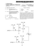
[0008] Referring to the FIGURE, an exemplary embodiment of an indication circuit is used for a computer system. The indication circuit includes three bipolar junction transistors (BJTs) Q1-Q3, seven resistors R1-R7, and two light-emitting diodes (LEDs) L1 and L2. In the embodiment, the LED L1 is a yellow LED, and the LED L2 is a green LED. The transistors Q1-Q3 are npn type BJTs.
[0009] A base of the BJT Q1 is connected to a general purpose input output (GPIO) pin GPIO1 on a motherboard through the resistor R1. A node between the resistor R1 and the GPIO pin GPIO1 is further connected to a power supply +3V_SB through the resistor R2. An emitter of the BJT Q1 is grounded. A collector of the BJT Q1 is connected to the power supply +3V_SB through the resistor R3. The collector of the BJT Q1 is further connected to a base of the BJT Q2. An emitter of the BJT Q2 is grounded. A collector of the BJT Q2 is connected to a power supply +5V_SB through the resistor R4. The collector of the BJT Q2 is connected to a cathode of the LED L1 and an anode of the LED L2.
[0010] A base of the BJT Q3 is connected to a GPIO pin GPIO2 on the motherboard through the resistor R5. Anode between the resistor R5 and the GPIO pin GPIO2 is further connected to the power supply +3V_SB through the resistor R6. An emitter of the BJT Q3 is grounded. A collector of the BJT Q3 is connected to the power supply +5V_SB through the resistor R7. The collector of the BJT Q3 is further connected to an anode of the LED L1 and a cathode of the LED L2.
[0011] Signals output from the GPIO pins GPIO1 and GPIO2, which can be set by the basic input output system (BIOS) are shown in Table 1 below:
TABLE-US-00001 TABLE 1 Signal from the Signal from the Errors GPIO pin GPIO1 GPIO pin GPIO2 Normal POST 1 1 RAM problem Blinking/1 Hz 1 Display or VGA card problem 0 Blinking/1 Hz Keyboard controller problem Blinking/0.5 Hz 1 Memory problem 0 Blinking/0.5 Hz
[0012] In the table 1 above, "0" stands for Low Level, "1" stands for High Level, "Blinking/1 Hz" stands for a frequency of the signal output from the GPIO pin is 1 Hz, and "Blinking/0.5 Hz" stands for a frequency of the signal output from the GPIO pin is 0.5 Hz.
[0013] When the computer system is working normally, the GPIO pins GPIO1 and GPIO2 output high level signals. In the condition, the BJTs Q1 and Q3 are turned on, and the BJT Q2 is turned off. As a result, the LED L1 is deactivated, and the LED L2 is activated. In other words, the indication circuit emits green lights.
[0014] When there are random-access memory (RAM) errors, the GPIO pin GPIO1 outputs a high level signal with a frequency of 1 Hz, and the GPIO pin GPIO2 outputs a high level signal. In this condition, the transistor Q3 is turned on. When the GPIO pin GPIO1 outputs a high level signal, the BJT Q1 is turned on, and the BJT Q2 is turned off. As a result, the LED L1 is deactivated, and the LED L2 is activated. In other words, the indication circuit emits green lights. When the GPIO pin GPIO1 does not output the high level signal, the BJT Q1 is turned off, and the BJT Q2 is turned on. As a result, the LEDs L1 and L2 are deactivated. In other words, the indication circuit emits no light. As a result, when there are RAM errors, the indication circuit blinks with green lights at a frequency of 1 Hz.
[0015] When there are display or video graphics array (VGA) card errors, the GPIO pin GPIO1 outputs a low level signal, and the GPIO pin GPIO2 outputs a high level signal with a frequency of 1 Hz. In this condition, the BJT Q1 is turned off, and the BJT Q2 is turned on. When the GPIO pin GPIO2 outputs a high level signal, the BJT Q3 is turned on. As a result, the LEDs L1 and L2 are deactivated. In other words, the indication circuit emits no light. When the GPIO pin GPIO2 does not output the high level signal, the BJT Q3 is turned off. As a result, the LED L1 is activated, and the LED L2 is deactivated. The indication circuit emits yellow lights. As a result, when there are display or VGA card errors of the computer system, the indication circuit blinks with yellow lights at a frequency of 1 Hz.
[0016] When there are keyboard controller errors, the GPIO pin GPIO1 outputs a high level signal with a frequency of 0.5 Hz, and the GPIO pin GPIO2 outputs a high level signal. In this condition, the BJT Q3 is turned on. When the GPIO pin GPIO1 outputs a high level signal, the BJT Q1 is turned on, and the BJT Q2 is turned off. As a result, the LED L1 is deactivated, and the LED L2 is activated. The indication circuit emits green lights. When the GPIO pin GPIO1 does not output the high level signal, the BJT Q1 is turned off, and the BJT Q2 is turned on. As a result, the LEDs L1 and L2 are deactivated. The indication circuit emits no light. As a result, when there are keyboard controller errors, the indication circuit blinks with green lights at a frequency of 0.5 Hz.
[0017] When there are memory errors, the GPIO pin GPIO1 outputs a low level signal, and the GPIO pin GPIO2 outputs a high level signal with a frequency of 0.5 Hz. In this condition, the BJT Q1 is turned off, and the BJT Q2 is turned on. When the GPIO pin GPIO2 outputs a high level signal, the BJT Q3 is turned on. As a result, the LEDs L1 and L2 are deactivated. The indication circuit emits no light. When the GPIO pin GPIO2 does not output the high level signal, the BJT Q3 is turned off. As a result, the LED L1 is activated, and the LED L2 is deactivated. The indication circuit emits yellow lights. As a result, when there are memory errors, the indication circuit blinks with yellow lights at a frequency of 0.5 Hz.
[0018] In the embodiment, the BJTs Q1-Q3 function as electronic switches. Moreover, the signals output from the GPIO pins GPIO1 and GPIO2 as shown in the table 1 are defined by users. In other embodiments, the signals output from the GPIO pins GPIO1 and GPIO2 can be different from the signals shown in table 1.
[0019] The LEDs L1 and L2 flash in different colors or at different frequencies to indicate specific error conditions during POST.
[0020] The foregoing description of the exemplary embodiments of the disclosure has been presented only for the purposes of illustration and description and is not intended to be exhaustive or to limit the disclosure to the precise forms disclosed. Many modifications and variations are possible in the light of everything above. The embodiments were chosen and described in order to explain the principles of the disclosure and their practical application so as to enable others of ordinary skill in the art to utilize the disclosure and various embodiments with various modifications as are suited to the particular use contemplated. Alternative embodiments will become apparent to those of ordinary skills in the art to which the present disclosure pertains without departing from its spirit and scope. Accordingly, the scope of the present disclosure is defined by the appended claims rather than the foregoing description and the exemplary embodiments described therein.
User Contributions:
Comment about this patent or add new information about this topic:
| People who visited this patent also read: | |
| Patent application number | Title |
|---|---|
| 20220150377 | IMAGE FORMING APPARATUS, CONTROL METHOD, AND STORAGE MEDIUM |
| 20220150376 | IMAGE FORMING APPARATUS |
| 20220150375 | IMAGE PROCESSING APPARATUS AND IMAGE PROCESSING METHOD |
| 20220150374 | IMAGE PROCESSING DEVICE, IMAGE READING DEVICE, IMAGE PROCESSING METHOD, AND NON-TRANSITORY COMPUTER READABLE MEDIUM |
| 20220150373 | IMAGE PROCESSING APPARATUS |
Images included with this patent application:
 |  |
| Similar patent applications: | |
| Date | Title |
|---|---|
| 2013-12-19 | Wireless proportional flow indication for a tire inflation system |
| 2013-12-19 | Method and apparatus for providing peak detection circuitry for data communication systems |
| 2011-03-10 | Overcurrent protection circuit |
| 2013-12-19 | Mobile terminal with location information acquiring portion |
| 2013-12-19 | Powerline communication diversity coupling technique |
| New patent applications in this class: | |
| Date | Title |
|---|---|
| 2019-05-16 | Color blind friendly pick to light system for identifying storage locations |
| 2016-06-30 | Guided installation for an opening sensor |
| 2016-06-16 | Configurable indicator on computing device |
| 2016-05-05 | Indicator module for modular computing units |
| 2016-04-28 | Method and evaluation device for evaluation of signals from a led status indicator |
| New patent applications from these inventors: | |
| Date | Title |
|---|---|
| 2013-10-03 | Power good signal generating circuit |
| 2013-09-19 | Indicator light control device |
| 2013-06-13 | Circuit for removing passwords |
| Top Inventors for class "Communications: electrical" | |
| Rank | Inventor's name |
|---|---|
| 1 | Lowell L. Wood, Jr. |
| 2 | Roderick A. Hyde |
| 3 | Juan Manuel Cruz-Hernandez |
| 4 | John R. Tuttle |
| 5 | Jordin T. Kare |